 | –≠–ª–µ–∫—Ç—Ä–æ–Ω–Ω—ã–π –∫–æ–º–ø–æ–Ω–µ–Ω—Ç: MT16D832X | –°–∫–∞—á–∞—Ç—å:  PDF PDF  ZIP ZIP |
Document Outline
- Features
- Options
- Part Numbers
- Pin Assignment (Front View) 72-Pin SIMM
- Key Timing Parameters
- General Description
- Fast Page Mode
- EDO Page Mode
- Refresh
- x16 Configuration
- JEDEC-Defined Presence-Detect - MT8D432(X) (16MB)
- JEDEC-Defined Presence-Detect - MT16D832(X) (32MB)
- Functional Block Diagrams
- MT8D432(X) (16MB)
- MT16D832(X) (32MB)
- Absolute Maximum Ratings
- DC Electrical Characteristics and Operating Conditions
- ICC Specifications and Conditions
- Capacitance
- Fast Page Mode AC Electrical Characteristics
- EDO Page Mode AC Electrical Characteristics
- Notes
- Read Cycle (FAST PAGE MODE Module)
- Read Cycle (EDO PAGE MODE Module)
- Early Write Cycle
- Fast-Page-Mode Read Cycle
- EDO-Page-Mode Read Cycle
- Fast-Page-Mode Early-Write Cycle
- EDO-Page-Mode Early-Write Cycle
- EDO-Page-Mode Read-Early-Write Cycle
- Fast-Page-Mode Read-Early-Write Cycle
- EDO Read Cycle
- RAS#-Only Refresh Cycle
- CBR Refresh Cycle
- Hidden Refresh Cycle
- 72-Pin SIMM (16MB)
- 72-Pin SIMM (32MB)

4, 8 Meg x 32 DRAM SIMMs
Micron Technology, Inc., reserves the right to change products or specifications without notice.
DM44_2.p65 ≠ Rev. 9/98
©1998, Micron Technology, Inc.
1
4, 8 MEG x 32
DRAM SIMMs
NOT RECOMMENDED FOR NEW DESIGNS
DRAM
MODULE
MT8D432(X)
MT16D832(X)
For the latest data sheet revisions, please refer to the
Micron Web site:
www.micron.com/datasheets
FEATURES
∑ JEDEC- and industry-standard pinout in a 72-pin,
single in-line memory module (SIMM)
∑ 16MB (4 Meg x 32) and 32MB (8 Meg x 32)
∑ High-performance CMOS silicon-gate process
∑ Single 5V ±10% power supply
∑ All inputs, outputs and clocks are TTL-compatible
∑ Refresh modes: RAS#-ONLY, CAS#-BEFORE-RAS#
(CBR) and HIDDEN
∑ 2,048-cycle refresh distributed across 32ms
∑ FAST PAGE MODE (FPM) access or
Extended Data-Out (EDO) PAGE MODE access
OPTIONS
MARKING
∑ Timing
50ns access
-5**
60ns access
-6
∑ Packages
72-pin SIMM
M
72-pin SIMM (Gold)
G
∑ Operating Modes
FAST PAGE MODE
None
EDO PAGE MODE
X
**EDO version only
PIN ASSIGNMENT (Front View)
72-Pin SIMM
4 Meg x 32
8 Meg x 32
PIN SYMBOL
PIN SYMBOL
PIN SYMBOL
PIN SYMBOL
1
Vss
19
A10
37
NC
55
DQ12
2
DQ1
20
DQ5
38
NC
56
DQ28
3
DQ17
21
DQ21
39
Vss
57
DQ13
4
DQ2
22
DQ6
40
CAS0#
58
DQ29
5
DQ18
23
DQ22
41
CAS2#
59
V
DD
6
DQ3
24
DQ7
42
CAS3#
60
DQ30
7
DQ19
25
DQ23
43
CAS1#
61
DQ14
8
DQ4
26
DQ8
44
RAS0#
62
DQ31
9
DQ20
27
DQ24
45
NC/RAS1#*
63
DQ15
10
V
DD
28
A7
46
NC
64
DQ32
11
NC
29
NC (
A11
)
47
WE#
65
DQ16
12
A0
30
V
DD
48
NC
66
NC
13
A1
31
A8
49
DQ9
67
PRD1
14
A2
32
A9
50
DQ25
68
PRD2
15
A3
33
NC/RAS3#*
51
DQ10
69
PRD3
16
A4
34
RAS2#
52
DQ26
70
PRD4
17
A5
35
NC
53
DQ11
71
NC
18
A6
36
NC
54
DQ27
72
Vss
*32MB version only
PART NUMBERS
EDO Operating Mode
PART NUMBER
CONFIGURATION
PLATING
MT8D432G- x X
4 Meg x 32
Gold
MT8D432M- x X
4 Meg x 32
Tin/Lead
MT16D832G-x X
8 Meg x 32
Gold
MT16D832M-x X
8 Meg x 32
Tin/Lead
x = speed
FPM Operating Mode
PART NUMBER
CONFIGURATION
PLATING
MT8D432G-x
4 Meg x 32
Gold
MT8D432M-x
4 Meg x 32
Tin/Lead
MT16D832G-x
8 Meg x 32
Gold
MT16D832M-x
8 Meg x 32
Tin/Lead
x = speed
NOTE: Symbols in parentheses are not used on these
modules but may be used for other modules in
this product family. They are for reference only.
KEY TIMING PARAMETERS
EDO Operating Mode
SPEED
t
RC
t
RAC
t
PC
t
AA
t
CAC
t
CAS
-5
84ns
50ns
20ns
25ns
13ns
8ns
-6
104ns
60ns
25ns
30ns
15ns
10ns
FPM Operating Mode
SPEED
t
RC
t
RAC
t
PC
t
AA
t
CAC
t
RP
-6
110ns
60ns
35ns
30ns
15ns
40ns
4, 8 Meg x 32 DRAM SIMMs
Micron Technology, Inc., reserves the right to change products or specifications without notice.
DM44_2.p65 ≠ Rev. 9/98
©1998, Micron Technology, Inc.
2
4, 8 MEG x 32
DRAM SIMMs
NOT RECOMMENDED FOR NEW DESIGNS
JEDEC-DEFINED
PRESENCE-DETECT ≠
MT8D432(X) (16MB)
SYMBOL
PIN
-5*
-6
PRD1
67
V
SS
V
SS
PRD2
68
NC
NC
PRD3
69
V
SS
NC
PRD4
70
V
SS
NC
JEDEC-DEFINED
PRESENCE-DETECT ≠
MT16D832(X) (32MB)
SYMBOL
PIN
-5*
-6
PRD1
67
NC
NC
PRD2
68
V
SS
V
SS
PRD3
69
V
SS
NC
PRD4
70
V
SS
NC
*EDO version only
GENERAL DESCRIPTION
The MT8D432(X) and MT16D832(X) are randomly
accessed, 16MB and 32MB solid-state memories orga-
nized in a x32 configuration. During READ or WRITE
cycles, each bit is uniquely addressed through 22 ad-
dress bits that are entered 11 bits (A0-A10) at a time.
RAS# is used to latch the first 11 bits and CAS# the latter
11 bits. READ and WRITE cycles are selected with the
WE# input. A logic HIGH on WE# dictates read mode,
while a logic LOW on WE# dictates write mode. During
a WRITE cycle, data-in (D) is latched by the falling edge
of CAS#. Since WE# goes LOW prior to CAS# going LOW,
the output pin(s) remain open (High-Z) until the next
CAS# cycle.
FAST PAGE MODE
FAST-PAGE-MODE operations allow faster data op-
erations (READ or WRITE) within a row-address-de-
fined page boundary. The FAST-PAGE-MODE cycle is
always initiated with a row address strobed in by RAS#,
followed by a column address strobed in by CAS#. Ad-
ditional columns may be accessed by providing valid
column addresses, strobing CAS# and holding RAS#
LOW, thus executing faster memory cycles. Returning
RAS# HIGH terminates the FAST-PAGE-MODE opera-
tion.
EDO PAGE MODE
EDO PAGE MODE, designated by the "X" version, is
an accelerated FAST-PAGE-MODE cycle. The primary
advantage of EDO is the availability of data-out even
after CAS# goes back HIGH. EDO provides for CAS#
precharge time (
t
CP) to occur without the output data
going invalid. This elimination of CAS# output control
provides for pipelined READs.
FAST-PAGE-MODE modules have traditionally
turned the output buffers off (High-Z) with the rising
edge of CAS#. EDO operates like FAST-PAGE-MODE
READs, except data will be held valid or become valid
after CAS# goes HIGH, as long as RAS# and OE# are
held LOW. (Refer to the MT4C4M4E8 DRAM data sheet
for additional information on EDO functionality.)
REFRESH
Returning RAS# and CAS# HIGH terminates a
memory cycle and decreases chip current to a reduced
standby level. Also, the chip is preconditioned for the
next cycle during the RAS# HIGH time. Memory cell
data is retained in its correct state by maintaining
power and executing any RAS# cycle (READ, WRITE) or
RAS# REFRESH cycle (RAS#-ONLY, CBR or HIDDEN) so
that all 2,048 combinations of RAS# addresses are ex-
ecuted at least every 32ms, regardless of sequence.
The CBR REFRESH cycle will invoke the refresh counter
for automatic RAS# addressing.
x16 CONFIGURATION
For x16 applications, the corresponding DQ and
CAS# pins must be connected together (DQ1 to DQ17,
DQ2 to DQ18 and so forth, and CAS0# to CAS2# and
CAS1# to CAS3#). Each RAS# is then a bank select for
the x16 memory organization.
4, 8 Meg x 32 DRAM SIMMs
Micron Technology, Inc., reserves the right to change products or specifications without notice.
DM44_2.p65 ≠ Rev. 9/98
©1998, Micron Technology, Inc.
3
4, 8 MEG x 32
DRAM SIMMs
NOT RECOMMENDED FOR NEW DESIGNS
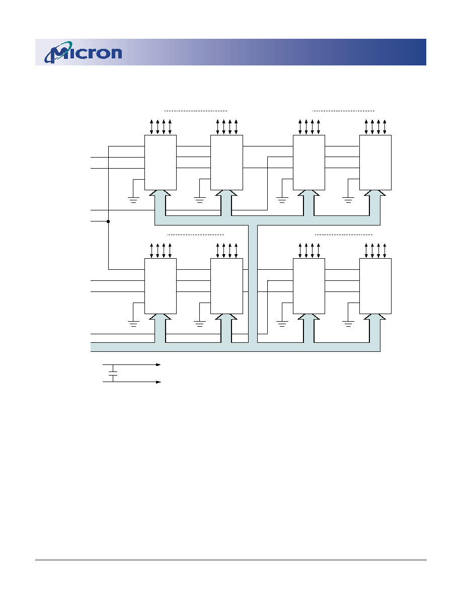
FUNCTIONAL BLOCK DIAGRAM
MT8D432(X) (16MB)
WE#
CAS#
RAS#
OE#
DQ1 - 4
U1
DQ1 - 4
DQ1
DQ8
DQ1 - 4
DQ1 - 4
DQ9
DQ16
CAS1#
WE#
DQ1 - 4
DQ1 - 4
DQ17
DQ24
DQ1 - 4
DQ1 - 4
DQ25
DQ32
CAS3#
U2
U5
U6
U3
U4
U7
U8
U1-U8 = 4 Meg x 4 DRAMs
A0-A10
A0-A10
11
A0-A10
A0-A10
A0-A10
A0-A10
A0-A10
A0-A10
A0-A10
CAS0#
RAS0#
CAS2#
RAS2#
11
11
11
11
11
11
11
11
WE#
CAS#
RAS#
OE#
WE#
CAS#
RAS#
OE#
WE#
CAS#
RAS#
OE#
WE#
CAS#
RAS#
OE#
WE#
CAS#
RAS#
OE#
WE#
CAS#
RAS#
OE#
WE#
CAS#
RAS#
OE#
V
DD
V
SS
U1-U8
U1-U8
4, 8 Meg x 32 DRAM SIMMs
Micron Technology, Inc., reserves the right to change products or specifications without notice.
DM44_2.p65 ≠ Rev. 9/98
©1998, Micron Technology, Inc.
4
4, 8 MEG x 32
DRAM SIMMs
NOT RECOMMENDED FOR NEW DESIGNS
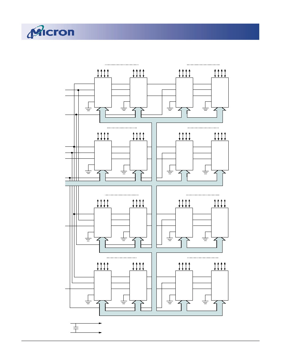
FUNCTIONAL BLOCK DIAGRAM
MT16D832(X) (32MB)
RAS3#
RAS1#
CAS3#
A0-A10
CAS1#
WE#
CAS#
RAS#
OE#
DQ1 - 4
U1
DQ1 - 4
DQ1
DQ8
DQ1 - 4
DQ1 - 4
DQ9
DQ16
DQ1 - 4
DQ1 - 4
DQ17
DQ24
DQ1 - 4
DQ1 - 4
DQ25
DQ32
U2
U5
U6
U3
U4
U7
U8
U1-U16 = 4 Meg x 4 DRAMs
DQ1 - 4
U9
DQ1 - 4
DQ1
DQ8
DQ1 - 4
DQ1 - 4
DQ9
DQ16
DQ1 - 4
DQ1 - 4
DQ17
DQ24
DQ1 - 4
DQ1 - 4
DQ25
DQ32
U10
U13
U14
U11
U12
U15
U16
A0-A10
A0-A10
A0-A10
A0-A10
A0-A10
A0-A10
A0-A10
A0-A10
A0-A10
A0-A10
A0-A10
A0-A10
A0-A10
A0-A10
A0-A10
A0-A10
CAS0#
RAS0#
CAS2#
RAS2#
WE#
11
11
11
11
11
11
11
11
11
11
11
11
11
11
11
11
WE#
CAS#
RAS#
OE#
WE#
CAS#
RAS#
OE#
WE#
CAS#
RAS#
OE#
WE#
CAS#
RAS#
OE#
WE#
CAS#
RAS#
OE#
WE#
CAS#
RAS#
OE#
WE#
CAS#
RAS#
OE#
WE#
CAS#
RAS#
OE#
WE#
CAS#
RAS#
OE#
WE#
CAS#
RAS#
OE#
WE#
CAS#
RAS#
OE#
WE#
CAS#
RAS#
OE#
WE#
CAS#
RAS#
OE#
WE#
CAS#
RAS#
OE#
WE#
CAS#
RAS#
OE#
V
DD
V
SS
U1-U16
U1-U16
4, 8 Meg x 32 DRAM SIMMs
Micron Technology, Inc., reserves the right to change products or specifications without notice.
DM44_2.p65 ≠ Rev. 9/98
©1998, Micron Technology, Inc.
5
4, 8 MEG x 32
DRAM SIMMs
NOT RECOMMENDED FOR NEW DESIGNS
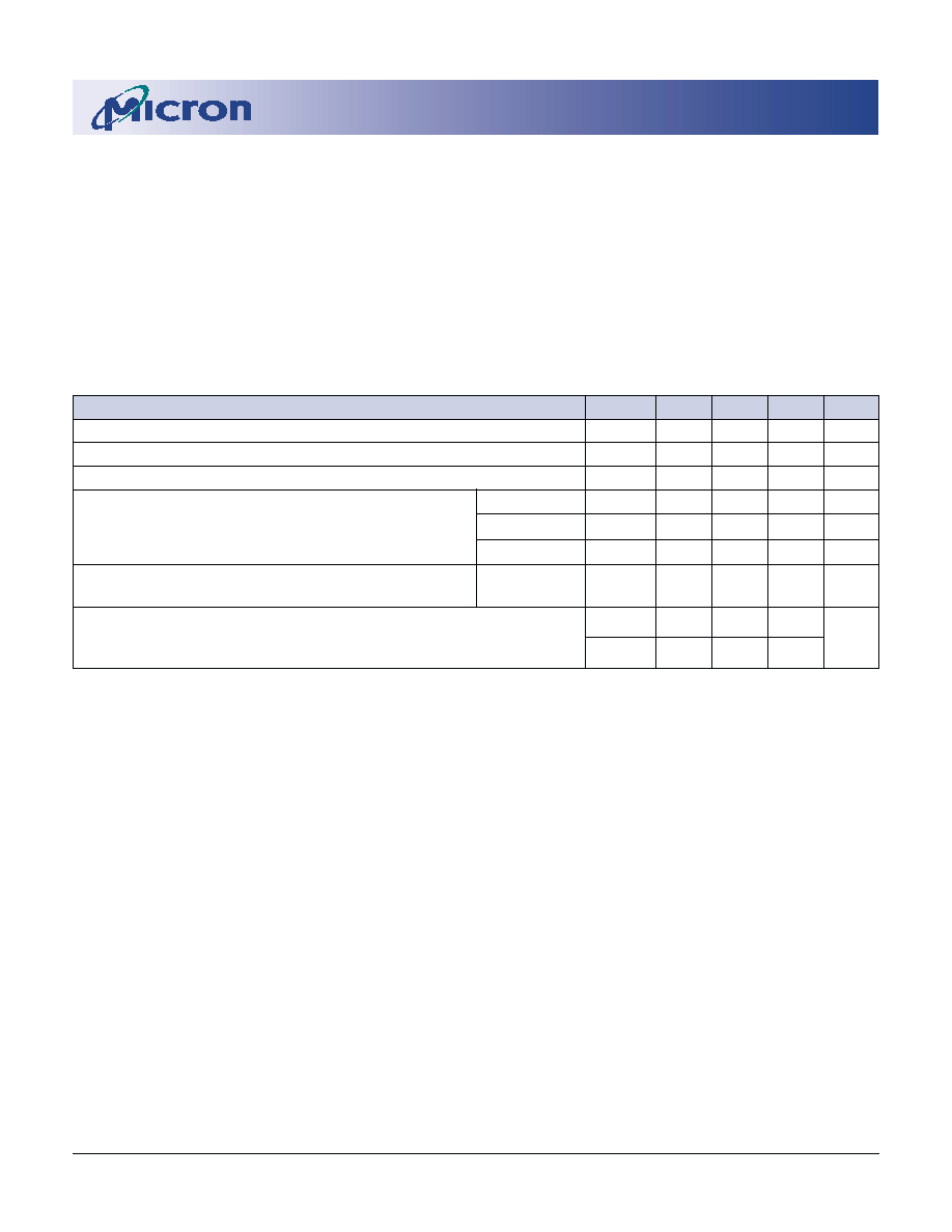
ABSOLUTE MAXIMUM RATINGS*
Voltage on Any Pin Relative to V
SS
................ -1V to +7V
Operating Temperature, T
A
(ambient) ... 0∞C to +70∞C
Storage Temperature (plastic) ............ -55∞C to +125∞C
Power Dissipation ........................................................ 8W
Short Circuit Output Current ................................. 50mA
*Stresses greater than those listed under "Absolute
Maximum Ratings" may cause permanent damage to
the device. This is a stress rating only and functional
operation of the device at these or any other conditions
above those indicated in the operational sections of
this specification is not implied. Exposure to absolute
maximum rating conditions for extended periods may
affect reliability.
DC ELECTRICAL CHARACTERISTICS AND OPERATING CONDITIONS
(Notes: 1) (V
DD
= +5V ±10%)
PARAMETER/CONDITION
SYMBOL MIN
MAX
UNITS NOTES
SUPPLY VOLTAGE
V
DD
4.5
5.5
V
INPUT HIGH VOLTAGE: Logic 1; All inputs
V
IH
2.4
V
DD
+ 1
V
INPUT LOW VOLTAGE: Logic 0; All inputs
V
IL
-1.0
0.8
V
INPUT LEAKAGE CURRENT:
RAS0#-RAS3#
I
I
1
-8
8
µA
Any input 0V
V
IN
5.5V
A0-A10, WE#
I
I
2
-32
32
µA
23
(All other pins not under test = 0V)
CAS0#-CAS3#
I
I
3
-8
8
µA
23
OUTPUT LEAKAGE CURRENT:
DQ1-DQ32
I
OZ
-10
10
µA
23
(DQ is disabled; 0V
V
OUT
5.5V)
OUTPUT LEVELS:
V
OH
2.4
≠
V
Output High Voltage (I
OUT
= -5mA)
Output Low Voltage (I
OUT
= 4.2mA)
V
OL
≠
0.4
V