1
8, 16, 32 Meg x 64 Nonbuffered DRAM DIMMs
Micron Technology, Inc., reserves the right to change products or specifications without notice.
DM78.p65 ≠ Rev. 2/99
©1999, Micron Technology, Inc.
8, 16, 32 MEG x 64
NONBUFFERED DRAM DIMMs
KEY TIMING PARAMETERS
SPEED
t
RC
t
RAC
t
PC
t
AA
t
CAC
t
CAS
-5
84ns
50ns
20ns
25ns
13ns
8ns
-6
104ns
60ns
25ns
30ns
15ns
10ns
DRAM
MODULE
MT8LD864A X, MT16LD1664A X,
MT32LD3264A X
For the latest data sheet, please refer to the Micron Web
site:
www.micronsemi.com/datasheets/datasheet.html
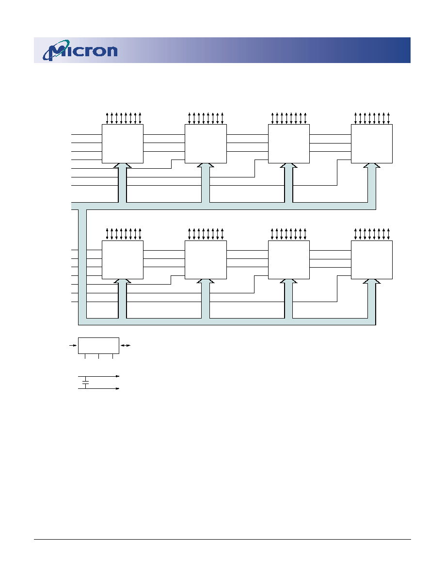
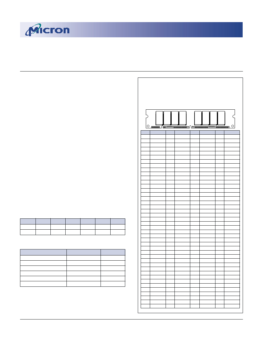
PIN ASSIGNMENT (Front View)
FEATURES
∑ Eight-CAS# ECC pinout in a 168-pin, dual in-line
memory module (DIMM)
∑ 64MB (8 Meg x 64), 128MB (16 Meg x 64), and
256MB (32 Meg x 64)
∑ Nonbuffered
∑ High-performance CMOS silicon-gate process
∑ Single +3.3V ±0.3V power supply
∑ All inputs, outputs and clocks are LVTTL-
compatible
∑ 4,096-cycle CAS#-BEFORE-RAS# (CBR) refresh
distributed across 64ms
∑ Extended Data-Out (EDO) PAGE MODE access cycle
∑ Serial presence-detect (SPD)
OPTIONS
MARKING
∑ Package
168-pin DIMM (gold)
G
∑ Timing
50ns access
-5
60ns access
-6
∑ Access Cycle
EDO PAGE MODE
X
PIN
SYMBOL
PIN
SYMBOL
PIN
SYMBOL
PIN
SYMBOL
1
V
SS
43
V
SS
85
V
SS
127
V
SS
2
DQ0
44
OE2#
86
DQ32
128
RFU
3
DQ1
45
RAS2#
87
DQ33
129 NC/RAS3#**
4
DQ2
46
CAS2#
88
DQ34
130
CAS6#
5
DQ3
47
CAS3#
89
DQ35
131
CAS7#
6
V
DD
48
WE2#
90
V
DD
132
RFU
7
DQ4
49
V
DD
91
DQ36
133
V
DD
8
DQ5
50
NC
92
DQ37
134
NC
9
DQ6
51
NC
93
DQ38
135
NC
10
DQ7
52
NC
94
DQ39
136
NC
11
DQ8
53
NC
95
DQ40
137
NC
12
V
SS
54
V
SS
96
V
SS
138
V
SS
13
DQ9
55
DQ16
97
DQ41
139
DQ48
14
DQ10
56
DQ17
98
DQ42
140
DQ49
15
DQ11
57
DQ18
99
DQ43
141
DQ50
16
DQ12
58
DQ19
100
DQ44
142
DQ51
17
DQ13
59
V
DD
101
DQ45
143
V
DD
18
V
DD
60
DQ20
102
V
DD
144
DQ52
19
DQ14
61
NC
103
DQ46
145
NC
20
DQ15
62
RFU
104
DQ47
146
RFU
21
NC
63
NC
105
NC
147
NC
22
NC
64
V
SS
106
NC
148
V
SS
23
V
SS
65
DQ21
107
V
SS
149
DQ53
24
NC
66
DQ22
108
NC
150
DQ54
25
NC
67
DQ23
109
NC
151
DQ55
26
V
DD
68
V
SS
110
V
DD
152
V
SS
27
WE0#
69
DQ24
111
RFU
153
DQ56
28
CAS0#
70
DQ25
112
CAS4#
154
DQ57
29
CAS1#
71
DQ26
113
CAS5#
155
DQ58
30
RAS0#
72
DQ27
114 NC/RAS1#**
156
DQ59
31
OE0#
73
V
DD
115
RFU
157
V
DD
32
V
SS
74
DQ28
116
V
SS
158
DQ60
33
A0
75
DQ29
117
A1
159
DQ61
34
A2
76
DQ30
118
A3
160
DQ62
35
A4
77
DQ31
119
A5
161
DQ63
36
A6
78
V
SS
120
A7
162
V
SS
37
A8
79
NC
121
A9
163
NC
38
A10
80
NC
122
A11
164
NC
39
NC (A12)
81
NC
123
NC (A13)
165
SA0
40
V
DD
82
SDA
124
V
DD
166
SA1
41
V
DD
83
SCL
125
RFU
167
SA2
42
RFU
84
V
DD
126
RFU
168
V
DD
** 256MB version only
168-Pin DIMM
(H-14; 64MB)
(H-17; 128MB)
(H-30; 256MB)
PART NUMBERS
PART NUMBER
CONFIGURATION
SPEED
MT8LD864AG-5 X
8 Meg x 64
50ns
MT8LD864AG-6 X
8 Meg x 64
60ns
MT16LD1664AG-5 X
16 Meg x 64
50ns
MT16LD1664AG-6 X
16 Meg x 64
60ns
MT32LD3264AG-5 X*
32 Meg x 64
50ns
MT32LD3264AG-6 X*
32 Meg x 64
60ns
*Contact factory for availability
NOTE:
Pin symbols in parentheses are not used on these modules but
may be used for other modules in this product family. They are
for reference only.
Micron is a registered trademark of Micron Technology, Inc.

2
8, 16, 32 Meg x 64 Nonbuffered DRAM DIMMs
Micron Technology, Inc., reserves the right to change products or specifications without notice.
DM78.p65 ≠ Rev. 2/99
©1999, Micron Technology, Inc.
8, 16, 32 MEG x 64
NONBUFFERED DRAM DIMMs
toggle from valid data to High-Z and back to the same
valid data. If OE# is toggled or pulsed after CAS# goes
HIGH while RAS# remains LOW, data will transition
to and remain High-Z.
During an application, if the DQ outputs are wire
OR'd, OE# must be used to disable idle banks of DRAMs.
Alternatively, pulsing WE# to the idle banks during
CAS# HIGH time will also tristate the outputs. Inde-
pendent of OE# control, the outputs will disable after
t
OFF, which is referenced from the rising edge of RAS#
or CAS#, whichever occurs last. (Refer to the 16 Meg x
4 [MT4LC16M4H9] DRAM data sheet for additional
information on EDO functionality.)
REFRESH
Returning RAS# and CAS# HIGH terminates a
memory cycle and decreases chip current to a reduced
standby level. Also, the chip is preconditioned for the
next cycle during the RAS# HIGH time. Correct memory
cell data is preserved by maintaining power and ex-
ecuting any RAS# cycle (READ, WRITE) or RAS# RE-
FRESH cycle (RAS#-ONLY, CBR or HIDDEN) so that all
combinations of RAS# addresses (A0-A10/A11) are
executed at least every
t
REF, regardless of sequence. The
CBR REFRESH cycle will invoke the internal refresh
counter for automatic RAS# addressing.
SERIAL PRESENCE-DETECT OPERATION
This module family incorporates serial presence-
detect (SPD). The SPD function is implemented using
a 2,048-bit EEPROM. This nonvolatile storage device
contains 256 bytes. The first 128 bytes can be pro-
grammed by Micron to identify the module type and
various DRAM organizations and timing parameters.
The remaining 128 bytes of storage are available for use
by the customer. System READ/WRITE operations be-
tween the master (system logic) and the slave EEPROM
device (DIMM) occur via a standard IIC bus using the
DIMM's SCL (clock) and SDA (data) signals, together
with SA(2:0), which provide 8 unique DIMM/EEPROM
addresses.
GENERAL DESCRIPTION
The Micron
Æ
MT8LD864A X, MT16LD1664A X
and MT32LD3264A X are randomly accessed 64MB,
128MB and 256MB memories organized in a x64 con-
figuration. They are specially processed to operate
from 3V to 3.6V for low-voltage memory systems.
During READ or WRITE cycles, each bit is uniquely
addressed through the 22/23 address bits, which are
entered 12 bits (A0-A11) at RAS# time and 11/12 bits
(A0-A11) at CAS# time.
READ and WRITE cycles are selected with the WE#
input. A logic HIGH on WE# dictates read mode, while
a logic LOW on WE# dictates write mode. During a
WRITE cycle, data-in (D) is latched by the falling edge
of WE# or CAS#, whichever occurs last. An EARLY
WRITE occurs when WE# is taken LOW prior to CAS#
falling. A LATE WRITE or READ-MODIFY-WRITE oc-
curs when WE# falls after CAS# was taken LOW.
During EARLY WRITE cycles, the data-outputs (Q) will
remain High-Z regardless of the state of OE#. During
LATE WRITE or READ-MODIFY-WRITE cycles, OE#
must be taken HIGH to disable the data-outputs prior
to applying input data. If a LATE WRITE or READ-
MODIFY-WRITE is attempted while keeping OE# LOW,
no WRITE will occur, and the data-outputs will drive
read data from the accessed location.
EDO PAGE MODE
EDO PAGE MODE is an accelerated FAST-PAGE-
MODE cycle. The primary advantage of EDO is the
availability of data-out even after CAS# goes back
HIGH. EDO provides for CAS# precharge time (
t
CP) to
occur without the output data going invalid. This
elimination of CAS# output control provides for pipe-
line READs.
FAST-PAGE-MODE modules have traditionally
turned the output buffers off (High-Z) with the rising
edge of CAS#. EDO-PAGE-MODE DRAMs operate like
FAST-PAGE-MODE DRAMs, except data will remain
valid or become valid after CAS# goes HIGH during
READs, provided RAS# and OE# are held LOW. If OE#
is pulsed while RAS# and CAS# are LOW, data will