1, 2, 4 Meg x 64 Nonbuffered DRAM DIMMs
Micron Technology, Inc., reserves the right to change products or specifications without notice.
DM67.p65 ≠ Rev. 6/98
©
1998, Micron Technology, Inc.
1
1, 2, 4 MEG x 64
NONBUFFERED DRAM DIMMs
OBSOLETE
FEATURES
∑ JEDEC pinout in a 168-pin, dual in-line memory
module (DIMM)
∑ 8MB (1 Meg x 64), 16MB (2 Meg x 64) and
32MB (4 Meg x 64)
∑ Nonbuffered
∑ High-performance CMOS silicon-gate process
∑ Single +3.3V
±
0.3V power supply
∑ All inputs, outputs and clocks are TTL-compatible
∑ Refresh modes: RAS#-ONLY, CAS#-BEFORE-RAS#
(CBR) and HIDDEN
∑ FAST-PAGE-MODE (FPM) or Extended Data-Out
(EDO) PAGE MODE access cycles
∑ 1,024-cycle refresh (10 row, 10 column addresses)
[MT4LD(T)164A(X)]
2,048-cycle refresh (11 row, 10 column addresses)
[MT8LD264A(X)]
2,048-cycle refresh (11 row, 11 column addresses)
[MT16LD464A(X)]
∑ Serial presence-detect (SPD)
OPTIONS
MARKING
∑ Components
SOJ
D
TSOP (1 Meg x 64 only)
DT
∑ Package
168-pin DIMM (gold)
G
∑ Timing
50ns access
-5*
60ns access
-6
∑ Access Cycles
FAST PAGE MODE
None
EDO PAGE MODE
X
*EDO version only
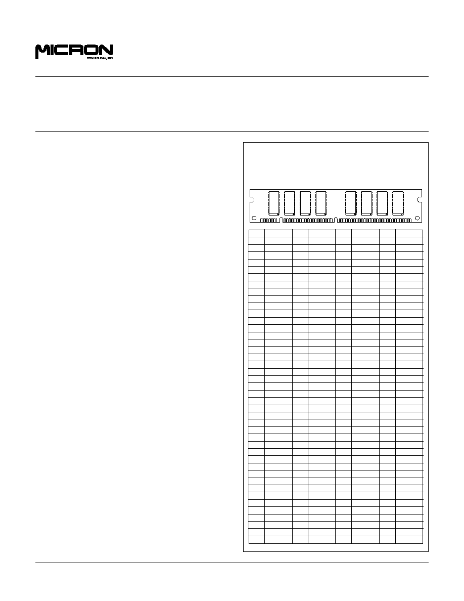
PIN
SYMBOL
PIN
SYMBOL
PIN
SYMBOL
PIN
SYMBOL
1
V
SS
43
V
SS
85
V
SS
127
V
SS
2
DQ0
44
OE2#
86
DQ32
128
RFU
3
DQ1
45
RAS2#
87
DQ33
129
NC
4
DQ2
46
CAS2#
88
DQ34
130
CAS6#
5
DQ3
47
CAS3#
89
DQ35
131
CAS7#
6
V
DD
48
WE2#
90
V
DD
132
RFU
7
DQ4
49
V
DD
91
DQ36
133
V
DD
8
DQ5
50
NC
92
DQ37
134
NC
9
DQ6
51
NC
93
DQ38
135
NC
10
DQ7
52
NC
94
DQ39
136
NC
11
DQ8
53
NC
95
DQ40
137
NC
12
V
SS
54
V
SS
96
V
SS
138
V
SS
13
DQ9
55
DQ16
97
DQ41
139
DQ48
14
DQ10
56
DQ17
98
DQ42
140
DQ49
15
DQ11
57
DQ18
99
DQ43
141
DQ50
16
DQ12
58
DQ19
100
DQ44
142
DQ51
17
DQ13
59
V
DD
101
DQ45
143
V
DD
18
V
DD
60
DQ20
102
V
DD
144
DQ52
19
DQ14
61
NC
103
DQ46
145
NC
20
DQ15
62
RFU
104
DQ47
146
RFU
21
NC
63
NC
105
NC
147
NC
22
NC
64
V
SS
106
NC
148
V
SS
23
V
SS
65
DQ21
107
V
SS
149
DQ53
24
NC
66
DQ22
108
NC
150
DQ54
25
NC
67
DQ23
109
NC
151
DQ55
26
V
DD
68
V
SS
110
V
DD
152
V
SS
27
WE0#
69
DQ24
111
RFU
153
DQ56
28
CAS0#
70
DQ25
112
CAS4#
154
DQ57
29
CAS1#
71
DQ26
113
CAS5#
155
DQ58
30
RAS0#
72
DQ27
114
NC
156
DQ59
31
OE0#
73
V
DD
115
RFU
157
V
DD
32
V
SS
74
DQ28
116
V
SS
158
DQ60
33
A0
75
DQ29
117
A1
159
DQ61
34
A2
76
DQ30
118
A3
160
DQ62
35
A4
77
DQ31
119
A5
161
DQ63
36
A6
78
V
SS
120
A7
162
V
SS
37
A8
79
NC
121
A9
163
NC
38
NC**/A10
80
NC
122
NC (A11)
164
NC
39
NC (A12)
81
NC
123
NC (A13)
165
SA0
40
V
DD
82
SDA
124
V
DD
166
SA1
41
V
DD
83
SCL
125
RFU
167
SA2
42
RFU
84
V
DD
126
RFU
168
V
DD
**1 Meg x 64 version only
PIN ASSIGNMENT (Front View)
168-Pin DIMM
DRAM
MODULE
MT4LDT164A(X), MT8LD264A(X),
MT16LD464A(X)
For the latest data sheet revisions, please refer to the Micron
Web site: www.micron.com/mti/msp/html/datasheet.html
NOTE: Pin symbols in parentheses are not used on these modules but may be used
for other modules in this product family. They are for reference only.
1, 2, 4 Meg x 64 Nonbuffered DRAM DIMMs
Micron Technology, Inc., reserves the right to change products or specifications without notice.
DM67.p65 ≠ Rev. 6/98
©
1998, Micron Technology, Inc.
2
1, 2, 4 MEG x 64
NONBUFFERED DRAM DIMMs
OBSOLETE
by a column address strobed in by CAS#. Additional col-
umns may be accessed by providing valid column
addresses, strobing CAS# and holding RAS# LOW , thus
executing faster memory cycles. Returning RAS# HIGH
terminates the FAST-PAGE-MODE operation.
EDO PAGE MODE
EDO PAGE MODE, designated by the "X" version, is an
accelerated FAST-PAGE-MODE cycle. The primary advan-
tage of EDO is the availability of data-out even after CAS#
goes back HIGH. EDO provides for CAS# precharge time
(
t
CP) to occur without the output data going invalid. This
elimination of CAS# output control provides for pipeline
READs.
FAST-PAGE-MODE modules have traditionally turned
the output buffers off (High-Z) with the rising edge of
CAS#. EDO-PAGE-MODE DRAMs operate like FAST-
PAGE-MODE DRAMs, except data will remain valid or
become valid after CAS# goes HIGH during READs, pro-
vided RAS# and OE# are held LOW. If OE# is pulsed while
RAS# and CAS# are LOW, data will toggle from valid data
to High-Z and back to the same valid data. If OE# is toggled
or pulsed after CAS# goes HIGH while RAS# remains
LOW, data will transition to and remain High-Z.
During an application, if the DQ outputs are wire OR'd,
OE# must be used to disable idle banks of DRAMs. Alterna-
tively, pulsing WE# to the idle banks during CAS# HIGH
time will also High-Z the outputs. Independent of OE#
control, the outputs will disable after
t
OFF, which is refer-
enced from the rising edge of RAS# or CAS#, whichever
occurs last. (Refer to the 4 Meg x 4 (MT4LC4M4E8) DRAM
data sheet for additional information on EDO functional-
ity.)
SERIAL PRESENCE-DETECT OPERATION
This module family incorporates serial presence-detect
(SPD). The SPD function is implemented using a 2,048-bit
EEPROM. This nonvolatile storage device contains 256
bytes. The first 128 bytes can be programmed by Micron to
identify the module type and various DRAM organizations
and timing parameters. The remaining 128 bytes of storage
are available for use by the customer. System READ/
WRITE operations between the master (system logic) and
the slave EEPROM device (DIMM) occur via a standard IIC
bus using the DIMM's SCL (clock) and SDA (data) signals,
together with SA(2:0), which provide eight unique DIMM/
EEPROM addresses.
KEY TIMING PARAMETERS
EDO Operating Mode
SPEED
t
RC
t
RAC
t
PC
t
AA
t
CAC
t
CAS
-5
84ns
50ns
20ns
25ns
13/15ns*
8ns
-6
104ns
60ns
25ns
30ns
15
10ns
*8MB DIMM
FPM Operating Mode
SPEED
t
RC
t
RAC
t
PC
t
AA
t
CAC
t
RP
-6
110ns
60ns
35ns
30ns
15ns
40ns
PART NUMBERS
EDO Operating Mode
PART NUMBER
CONFIGURATION
SPEED
PACKAGE
MT4LDT164AG-5 X
1 Meg x 64
50ns
TSOP
MT4LDT164AG-6 X
1 Meg x 64
60ns
TSOP
MT8LD264AG-5 X
2 Meg x 64
50ns
SOJ
MT8LD264AG-6 X
2 Meg x 64
60ns
SOJ
MT16LD464AG-5 X
4 Meg x 64
50ns
SOJ
MT16LD464AG-6 X
4 Meg x 64
60ns
SOJ
FPM Operating Mode
PART NUMBER
CONFIGURATION
SPEED
PACKAGE
MT4LDT164AG-6
1 Meg x 64
60ns
TSOP
MT8LD264AG-6
2 Meg x 64
60ns
SOJ
MT16LD464AG-6
4 Meg x 64
60ns
SOJ
GENERAL DESCRIPTION
The MT4LDT164A(X), MT8LD264A(X) and
MT16LD464A(X) are randomly accessed 8MB, 16MB and
32MB memories organized in a x64 configuration. During
READ or WRITE cycles, each bit is uniquely addressed
through the 20/21/22 address bits, which are entered 10/
11 bits (A0 -A10) at RAS# time and 10/11 bits (A0-A10) at
CAS# time.
FAST PAGE MODE
FAST-PAGE-MODE operations allow faster data opera-
tions (READ or WRITE) within a row-address-defined
page boundary. The FAST-PAGE-MODE cycle is always
initiated with a row address strobed in by RAS#, followed
1, 2, 4 Meg x 64 Nonbuffered DRAM DIMMs
Micron Technology, Inc., reserves the right to change products or specifications without notice.
DM67.p65 ≠ Rev. 6/98
©
1998, Micron Technology, Inc.
3
1, 2, 4 MEG x 64
NONBUFFERED DRAM DIMMs
OBSOLETE
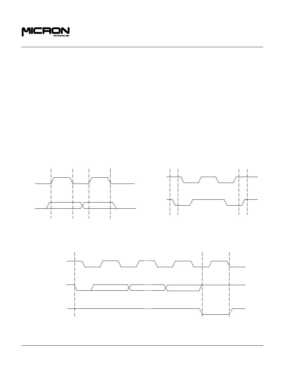
SPD ACKNOWLEDGE
Acknowledge is a software convention used to indicate
successful data transfers. The transmitting device, either
master or slave, will release the bus after transmitting eight
bits. During the ninth clock cycle, the receiver will pull the
SDA line LOW to acknowledge that it received the eight bits
of data (Figure 3).
The SPD device will always respond with an acknowl-
edge after recognition of a start condition and its slave
address. If both the device and a write operation have been
selected, the SPD device will respond with an acknowledge
after the receipt of each subsequent eight-bit word. In the
read mode the SPD device will transmit eight bits of data,
release the SDA line and monitor the line for an acknowl-
edge. If an acknowledge is detected and no stop condition
is generated by the master, the slave will continue to trans-
mit data. If an acknowledge is not detected, the slave will
terminate further data transmissions and await the stop
condition to return to standby power mode.
SPD CLOCK AND DATA CONVENTIONS
Data states on the SDA line can change only during SCL
LOW. SDA state changes during SCL HIGH are reserved
for indicating start and stop conditions (Figures 1 and 2).
SPD START CONDITION
All commands are preceded by the start condition, which
is a HIGH-to-LOW transition of SDA when SCL is HIGH.
The SPD device continuously monitors the SDA and SCL
lines for the start condition and will not respond to any
command until this condition has been met.
SPD STOP CONDITION
All communications are terminated by a stop condition,
which is a LOW-to-HIGH transition of SDA when SCL is
HIGH. The stop condition is also used to place the SPD
device into standby power mode.
SCL from Master
Data Output
from Transmitter
Data Output
from Receiver
9
8
Acknowledge
Figure 3
ACKNOWLEDGE RESPONSE FROM RECEIVER
Figure 1
DATA VALIDITY
Figure 2
DEFINITION OF START AND STOP
SCL
SDA
DATA STABLE
DATA STABLE
DATA
CHANGE
SCL
SDA
START
BIT
STOP
BIT
1, 2, 4 Meg x 64 Nonbuffered DRAM DIMMs
Micron Technology, Inc., reserves the right to change products or specifications without notice.
DM67.p65 ≠ Rev. 6/98
©
1998, Micron Technology, Inc.
4
1, 2, 4 MEG x 64
NONBUFFERED DRAM DIMMs
OBSOLETE
FUNCTIONAL BLOCK DIAGRAM
MT4LDT164A(X) (8MB)
DQ0-DQ15
DQ16-DQ31
DQ32-DQ47
DQ48-DQ63
A0-A9
OE2#
WE2#
CAS4#
RAS2#
CAS5#
CAS7#
CAS6#
U1-U4 = MT4LC1M16C3 FAST PAGE MODE
U1-U4 = MT4LC1M16E5 EDO PAGE MODE
OE0#
WE0#
CAS0#
RAS0#
CAS1#
CAS3#
CAS2#
10
10
10
10
10
DQ0-DQ15
U1
A0≠A9
WE#
OE#
RAS#
LCAS#
UCAS#
16
16
U2
A0≠A9
16
U3
16
U4
A0
SA0
SPD
SCL
SDA
A0≠A9
A0≠A9
A1
SA1
A2
SA2
WE#
OE#
RAS#
LCAS#
UCAS#
WE#
OE#
RAS#
LCAS#
UCAS#
WE#
OE#
RAS#
LCAS#
UCAS#
V
DD
V
SS
U1-U4
U1-U4
DQ0-DQ15
DQ0-DQ15
DQ0-DQ15
1, 2, 4 Meg x 64 Nonbuffered DRAM DIMMs
Micron Technology, Inc., reserves the right to change products or specifications without notice.
DM67.p65 ≠ Rev. 6/98
©
1998, Micron Technology, Inc.
5
1, 2, 4 MEG x 64
NONBUFFERED DRAM DIMMs
OBSOLETE
FUNCTIONAL BLOCK DIAGRAM
MT8LD264A(X) (16MB)
A0-A10
OE2#
WE2#
CAS4#
RAS2#
CAS5#
CAS7#
CAS6#
U6
U7
U8
U5
U2
U4
U3
DQ0-DQ7
U1
A0≠A10
WE#
OE#
RAS#
CAS#
A0≠A10
WE#
OE#
RAS#
CAS#
A0≠A10
WE#
OE#
RAS#
CAS#
A0≠A10
WE#
OE#
RAS#
CAS#
A0≠A10
WE#
OE#
RAS#
CAS#
A0≠A10
WE#
OE#
RAS#
CAS#
A0≠A10
WE#
OE#
RAS#
CAS#
A0≠A10
WE#
OE#
RAS#
CAS#
U1-U8 = MT4LC2M8B1 FAST PAGE MODE
U1-U8 = MT4LC2M8E7 EDO PAGE MODE
OE0#
WE0#
CAS0#
RAS0#
CAS1#
CAS3#
CAS2#
A0
SA0
SPD
SCL
SDA
A1
SA1
A2
SA2
11
11
11
11
11
11
11
11
11
V
DD
V
SS
U1-U8
U1-U8
DQ0-DQ7
DQ0-DQ7
DQ0-DQ7
DQ0-DQ7
DQ0-DQ7
DQ0-DQ7
DQ0-DQ7
DQ0-DQ7
DQ8-DQ15
DQ16-DQ23
DQ24-DQ31
DQ32-DQ39
DQ40-DQ47
DQ48-DQ55
DQ56-DQ63
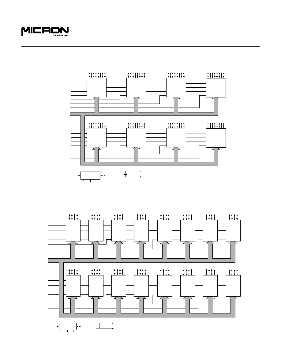
FUNCTIONAL BLOCK DIAGRAM
MT16LD464A(X) (32MB)
WE#
OE#
RAS#
CAS#
U1
A0≠A10
WE#
OE#
RAS#
CAS#
WE#
OE#
RAS#
CAS#
WE#
OE#
RAS#
CAS# A0≠A10
WE#
OE#
RAS#
CAS# A0≠A10
WE#
OE#
RAS#
CAS# A0≠A10
WE#
OE#
RAS#
CAS# A0≠A10
WE#
OE#
RAS#
CAS# A0≠A10
WE#
OE#
RAS#
CAS# A0≠A10
WE#
OE#
RAS#
CAS#
WE#
OE#
RAS#
CAS#
WE#
OE#
RAS#
CAS# A0≠A10
WE#
OE#
RAS#
CAS# A0≠A10
WE#
OE#
RAS#
CAS# A0≠A10
A0≠A10
A0≠A10
A0≠A10
A0≠A10
WE#
OE#
RAS#
CAS# A0≠A10
WE#
OE#
RAS#
CAS# A0≠A10
U2
U3
U4
U1-U16 = MT4LC4M4B1 FAST PAGE MODE
U1-U16 = MT4LC4M4E8 EDO PAGE MODE
U5
U6
U7
U8
11
11
11
11
11
11
11
11
11
U9
U10
U11
U12
U13
U14
U15
U16
11
11
11
11
11
11
11
11
OE0#
CAS1#
CAS2#
CAS3#
WE0#
CAS0#
OE2#
CAS5#
CAS6#
CAS7#
WE2#
CAS4#
A0-A10
RAS0#
RAS2#
A0
SA0
SPD
SCL
SDA
A1
SA1
A2
SA2
V
DD
V
SS
U1-U16
U1-U16
DQ0-DQ3
DQ4-DQ7
DQ8-DQ11
DQ12-DQ15
DQ16-DQ19
DQ20-DQ23
DQ24-DQ27
DQ28-DQ31
DQ32-DQ35
DQ36-DQ39
DQ40-DQ43
DQ44-DQ47
DQ48-DQ51
DQ52-DQ55
DQ56-DQ59
DQ60-DQ63
DQ0-DQ3
DQ0-DQ3
DQ0-DQ3
DQ0-DQ3
DQ0-DQ3
DQ0-DQ3
DQ0-DQ3
DQ0-DQ3
DQ0-DQ3
DQ0-DQ3
DQ0-DQ3
DQ0-DQ3
DQ0-DQ3
DQ0-DQ3
DQ0-DQ3
DQ0-DQ3