Document Outline
- Features
- Options
- Timing Parameters
- Address Table
- Part Numbers
- Pin Assignment
- Pin Locations
- Pin Descriptions
- Functional Block Diagram
- MT8LSDT864A (64MB)
- MT16LSDT1664A (128MB)
- General Description
- Serial Presence-Detect Operation
- Register Definition
- Initialization
- Mode Register
- Mode Register Definition Diagram
- Burst Length
- Burst Definition Table
- Burst Type
- CAS Latency Diagram
- CAS Latency Table
- CAS Latency
- Operating Mode
- Write Burst Mode
- Commands
- Truth Table - SDRAM Commands and DQMB Operation
- Absolute Maximum Ratings
- DC Electrical Characteristics and Operating Conditions - 64MB Module
- DC Electrical Characteristics and Operating Conditions - 128MB Module
- IDD Specifications and Conditions - 64MB Module
- IDD Specifications and Conditions - 128MB Module
- Capacitance (64MB)
- Capacitance (128MB)
- Electrical Characteristics and Recommended AC Operating Conditions
- AC Functional Characteristics
- Notes
- SPD Clock and Data Conventions
- SPD Start Conditions
- SPD Stop Condition
- SPD Acknowledge
- Figure 1 Data Validity
- Figure 2 Definition of Start and Stop
- Figure 3 Acknowledge Response from Receiver
- EEPROM Device Select Code
- EEPROM Operating Modes
- SPD EEPROM Timing Diagram
- Serial Presence-Detect EEPROM Timing Parameters
- Serial Presence-Detect EEPROM DC Operating Conditions
- Serial Presence-Detect EEPROM AC Operating Conditions
- Serial Presence-Detect Matrix
- 64MB Module
- 128MB Module
1
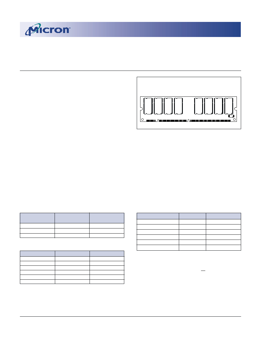
8, 16 Meg x 64 SDRAM DIMMs
Micron Technology, Inc., reserves the right to change products or specifications without notice.
SD8_16C8_16X64AG_A.p65 ≠ Rev. A, Pub. 4/02
©2002, Micron Technology, Inc.
64MB / 128MB (x64)
168-PIN SDRAM DIMMs
TIMING PARAMETERS
Module
PC100
PC133
Markings
CL -
t
RCD -
t
RP
CL -
t
RCD -
t
RP
-13E
2 - 2 - 2
2 - 2 - 2
-133
2 - 2 - 2
3 - 3 - 3
-10E
2 - 2 - 2
NA
SYNCHRONOUS
DRAM MODULE
MT8LSDT864A - 64MB
MT16LSDT1664A - 128MB
For the latest data sheet, please refer to the Micron Web
site:
www.micron.com/moduleds
FEATURES
∑ PC100 and PC133 compliant
∑ JEDEC-standard 168-pin, dual in-line memory
module (DIMM)
∑ Utilizes 100 MHz and 133 MHz SDRAM components
∑ Unbuffered
∑ 64MB (8 Meg x 64), 128MB (16 Meg x 64)
∑ Single +3.3V ±0.3V power supply
∑ Fully synchronous; all signals registered on
positive edge of system clock
∑ Internal pipelined operation; column address can
be changed every clock cycle
∑ Internal SDRAM banks for hiding row access/
precharge
∑ Programmable burst lengths: 1, 2, 4, 8, or full page
∑ Auto precharge, auto refresh, and self refresh
modes
∑ 64ms, 4,096-cycle refresh (15.625µs refresh
interval)
∑ LVTTL-compatible inputs and outputs
∑ Serial Presence-Detect (SPD)
ADDRESS TABLE
64MB Module
128MB Module
Refresh Count
4K
4K
Device Banks
4 (BA0, BA1)
4 (BA0, BA1)
Device Configuration
8 Meg x 8
8 Meg x 8
Row Addressing
4K (A0≠A11)
4K (A0≠A11)
Column Addressing
512 (A0≠A8)
512 (A0≠A8)
Module Banks
1 (S0,S2)
2 (S0,S2; S1,S3)
PART NUMBERS
PART NUMBER
CONFIGURATION SYSTEM BUS SPEED
MT8LSDT864AG-13E_
8 Meg x 64
133 MHz
MT8LSDT864AG-133_
8 Meg x 64
133 MHz
MT8LSDT864AG-10E_
8 Meg x 64
100 MHz
MT16LSDT1664AG-13E_
16 Meg x 64
133 MHz
MT16LSDT1664AG-133_
16 Meg x 64
133 MHz
MT16LSDT1664AG-10E_
16 Meg x 64
100 MHz
NOTE: The designators for component and PCB revision are the
last two characters of each part number Consult
factory for current revision codes.
Example: MT16LSDT1664AG-133B1.
168-Pin DIMM
MO168
OPTIONS
MARKING
∑ Package
168-pin DIMM (gold)
G
∑ Memory Clock/CAS Latency
7.5ns (133 MHz)/CL = 2
-13E
7.5ns (133 MHz)/CL = 3
-133
10ns (100 MHz)/CL = 2
-10E
2
8, 16 Meg x 64 SDRAM DIMMs
Micron Technology, Inc., reserves the right to change products or specifications without notice.
SD8_16C8_16X64AG_A.p65 ≠ Rev. A, Pub. 4/02
©2002, Micron Technology, Inc.
64MB / 128MB (x64)
168-PIN SDRAM DIMMs
PIN SYMBOL PIN SYMBOL
PIN
SYMBOL
PIN
SYMBOL
85
V
SS
106
DNU
127
V
SS
148
V
SS
86
DQ32
107
V
SS
128
CKE0
149
DQ53
87
DQ33
108
NC
129
S3#
150
DQ54
88
DQ34
109
NC
130
DQMB6
151
DQ55
89
DQ35
110
V
DD
131
DQMB7
152
V
SS
90
V
DD
111
CAS#
132
NC
153
DQ56
91
DQ36
112 DQMB4
133
V
DD
154
DQ57
92
DQ37
113 DQMB5
134
NC
155
DQ58
93
DQ38
114
S1#
135
NC
156
DQ59
94
DQ39
115
RAS#
136
DNU
157
V
DD
95
DQ40
116
V
SS
137
DNU
158
DQ60
96
V
SS
117
A1
138
V
SS
159
DQ61
97
DQ41
118
A3
139
DQ48
160
DQ62
98
DQ42
119
A5
140
DQ49
161
DQ63
99
DQ43
120
A7
141
DQ50
162
V
SS
100
DQ44
121
A9
142
DQ51
163
CK3
101
DQ45
122
BA0
143
V
DD
164
NC
102
V
DD
123
A11
144
DQ52
165
SA0
103
DQ46
124
V
DD
145
NC
166
SA1
104
DQ47
125
CK1
146
NC
167
SA2
105
DNU
126
NC
147
NC
168
V
DD
PIN SYMBOL PIN SYMBOL
PIN
SYMBOL
PIN
SYMBOL
1
V
SS
22
DNU
43
V
SS
64
V
SS
2
DQ0
23
V
SS
44
NC
65
DQ21
3
DQ1
24
NC
45
S2#
66
DQ22
4
DQ2
25
NC
46
DQMB2
67
DQ23
5
DQ3
26
V
DD
47
DQMB3
68
V
SS
6
V
DD
27
WE#
48
NC
69
DQ24
7
DQ4
28
DQMB0
49
V
DD
70
DQ25
8
DQ5
29
DQMB1
50
NC
71
DQ26
9
DQ6
30
S0#
51
NC
72
DQ27
10
DQ7
31
NC
52
DNU
73
V
DD
11
DQ8
32
V
SS
53
DNU
74
DQ28
12
V
SS
33
A0
54
V
SS
75
DQ29
13
DQ9
34
A2
55
DQ16
76
DQ30
14
DQ10
35
A4
56
DQ17
77
DQ31
15
DQ11
36
A6
57
DQ18
78
V
SS
16
DQ12
37
A8
58
DQ19
79
CK2
17
DQ13
38
A10
59
V
DD
80
NC
18
V
DD
39
BA1
60
DQ20
81
NC
19
DQ14
40
V
DD
61
NC
82
SDA
20
DQ15
41
V
DD
62
NC
83
SCL
21
DNU
42
CK0
63
CKE1
84
V
DD
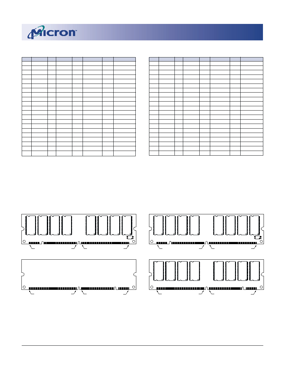
PIN ASSIGNMENT (168-PIN DIMM FRONT)
PIN ASSIGNMENT (168-Pin DIMM BACK)
PIN LOCATIONS (168-PIN DIMM)
U1
U2
U3
U4
U6
U7
U8
U9
U10
PIN 1
PIN 84
PIN 168
PIN 85
Front View
Back View
PIN 40
PIN 41
PIN 125
PIN 124
U1
U2
U3
U4
U6
U7
U8
U9
U10
U11
U12
U13
U14
U16
U17
U18
U19
PIN 1
PIN 84
PIN 168
PIN 85
Front View
Back View
PIN 40
PIN 41
PIN 125
PIN 124
No Components This Side of Module
64MB Module
128MB Module
3
8, 16 Meg x 64 SDRAM DIMMs
Micron Technology, Inc., reserves the right to change products or specifications without notice.
SD8_16C8_16X64AG_A.p65 ≠ Rev. A, Pub. 4/02
©2002, Micron Technology, Inc.
64MB / 128MB (x64)
168-PIN SDRAM DIMMs
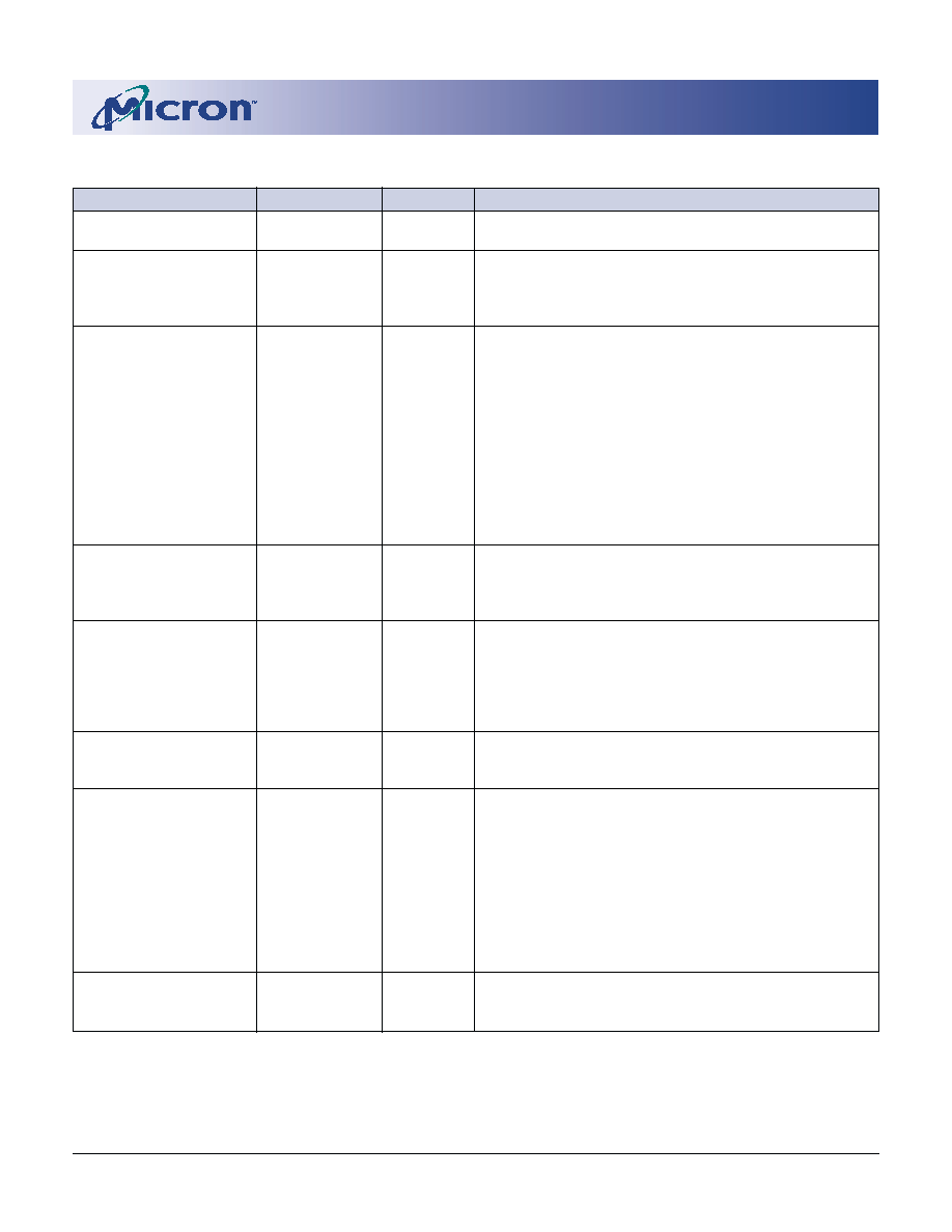
PIN DESCRIPTIONS
PIN NUMBERS
SYMBOL
TYPE
DESCRIPTION
27, 111, 115
RAS#, CAS#,
Input
Command Inputs: RAS#, CAS#, and WE# (along with
WE#
S#) define the command being entered.
42, 79, 125, 163
CK0-CK3
Input
Clock: CK is driven by the system clock. All SDRAM
input signals are sampled on the positive edge of CK.
CK also increments the internal burst counter and
controls the output registers.
63, 128
CKE0, CKE1
Input
Clock Enable: CKE activates (HIGH) and deactivates
(LOW) the CK signal. Deactivating the clock provides
PRECHARGE POWER-DOWN and SELF REFRESH
operation (all device banks idle), ACTIVE POWER-
DOWN (row ACTIVE in any device bank) or CLOCK
SUSPEND operation (burst access in progress). CKE is
synchronous except after the device enters power-
down and self refresh modes, where CKE becomes
asynchronous until after exiting the same mode. The
input buffers, including CK, are disabled during
power-down and self refresh modes, providing low
standby power.
30, 45, 114, 129
S0#-S3#
Input
Chip Select: S# enables (registered LOW) and disables
(registered HIGH) the command decoder. All com-
mands are masked when S# is registered HIGH. S# is
considered part of the command code.
28, 29, 46, 47,
DQMB0-DQMB7
Input
Input/Output Mask: DQMB is an input mask signal for
112, 113, 130, 131
write accesses and an output enable signal for read
accesses. Input data is masked when DQMB is sampled
HIGH during a WRITE cycle. The output buffers are
placed in a High-Z state (two-clock latency) when
DQMB is sampled HIGH during a READ cycle.
39, 122
BA0, BA1
Input
Bank Address: BA0 and BA1 define to which device
bank the ACTIVE, READ, WRITE, or PRECHARGE
command is being applied.
33, 34, 35, 36, 37, 38,
A0-A11
Input
Address Inputs: Provide the row address for ACTIVE
117, 118, 119, 120, 121,
commands, and the column addres and auto
123
precharge bit (A10) for READ/WRITE commands, to
select one location out of the memory array in the
respective device bank. A10 sampled during a
PRECHARGE command determines whether the
PRECHARGE applies to one device bank (A10 LOW,
device bank selected by BA0, BA1) or all device banks
(A10 HIGH). The address input also provide the
op-code during a MODE REGISTER SET command.
83
SCL
Input
Serial Clock for Presence-Detect: SCL is used to
synchronize the presence-detect data transfer to and
from the module.
NOTE: Pin numbers may not correlate with symbols. Refer to Pin Assignment tables for pin number and symbol information.
4
8, 16 Meg x 64 SDRAM DIMMs
Micron Technology, Inc., reserves the right to change products or specifications without notice.
SD8_16C8_16X64AG_A.p65 ≠ Rev. A, Pub. 4/02
©2002, Micron Technology, Inc.
64MB / 128MB (x64)
168-PIN SDRAM DIMMs
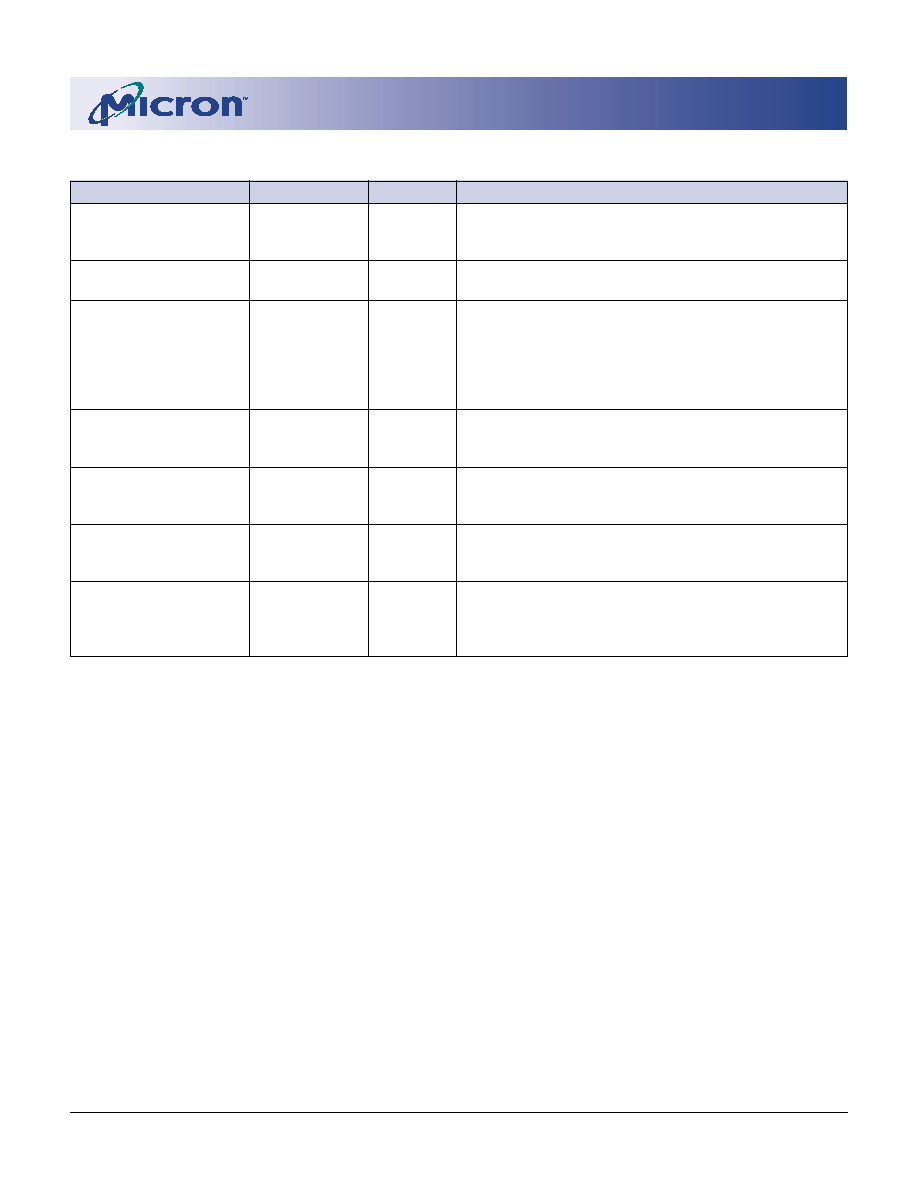
PIN DESCRIPTIONS (continued)
PIN NUMBERS
SYMBOL
TYPE
DESCRIPTION
82
SDA
Input/
Serial Presence-Detect Data: SDA is a bidirectional pin
Output
used to transfer addresses and data into and data out
of the presence-detect portion of the module.
165, 166, 167
SA0, SA1, SA2
Input
Presence-Detect Address Inputs: These pins are used
to configure the presence-detect device.
2-5, 7-11, 13-17, 19, 20,
DQ0-DQ63
Input/
Data I/O: Data bus.
55-58, 60, 65-67, 69-72,
Output
74-77, 86-89, 91-95,
97-101, 103, 104, 139-142,
144, 149-151, 153-156,
158-161
6, 18, 26, 40, 41, 49, 59,
V
DD
Supply
Power Supply: +3.3V ±0.3V.
73, 84, 90, 102, 110,
124, 133, 143, 157, 168
1, 12, 23, 32, 43, 54, 64,
V
SS
Supply
Ground.
68, 78, 85, 96, 107, 116,
127, 138, 148, 152, 162
21, 22, 52, 53, 105, 106
DNU
≠
Do Not Use: These pins are not connected on this
136, 137
module, but are assigned pins on other modules in
this product family.
24, 25, 31, 44, 48, 50, 51
NC
≠
Not Connected: These pins are not connected on this
61, 62, 80, 81, 108, 109,
module.
126, 132, 134, 135, 145,
146, 147, 164
NOTE: Pin numbers may not correlate with symbols. Refer to Pin Assignment tables for pin number and symbol information.
5
8, 16 Meg x 64 SDRAM DIMMs
Micron Technology, Inc., reserves the right to change products or specifications without notice.
SD8_16C8_16X64AG_A.p65 ≠ Rev. A, Pub. 4/02
©2002, Micron Technology, Inc.
64MB / 128MB (x64)
168-PIN SDRAM DIMMs
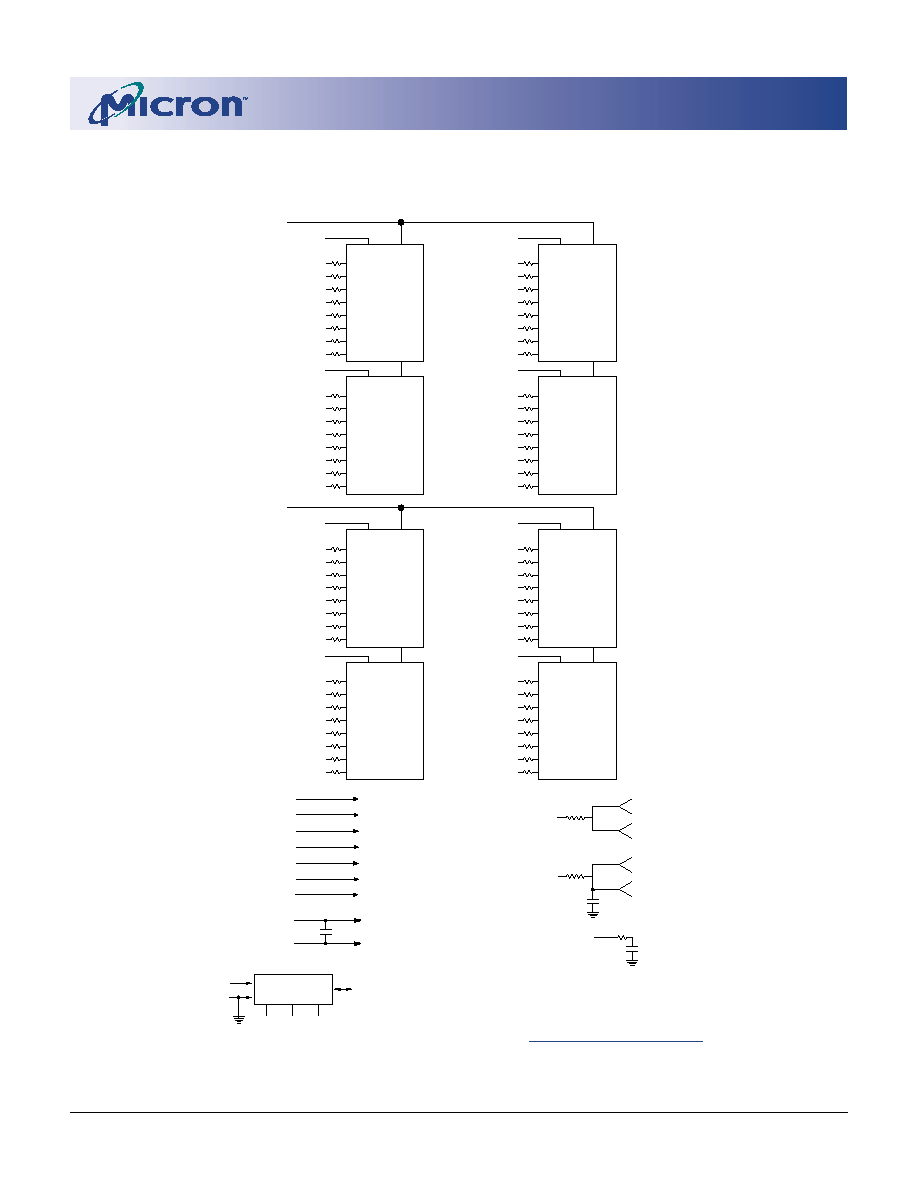
FUNCTIONAL BLOCK DIAGRAM
MT8LSDT864A (64MB)
NOTE: 1. All resistor values are 10 ohms unless otherwise specified.
2. Reference designators in this diagram do not necessarily match the actual module.
DQM CS#
U8
SDRAMs = MT48LC8M8A2TG for MT8LSDT864AG
A0
SA0
SPD
SDA
A1
SA1
A2
SA2
DQ56
DQ57
DQ58
DQ59
DQ60
DQ61
DQ62
DQ63
DQMB7
DQM CS#
U6
DQ48
DQ49
DQ50
DQ51
DQ52
DQ53
DQ54
DQ55
DQMB6
DQM CS#
U4
DQ40
DQ41
DQ42
DQ43
DQ44
DQ45
DQ46
DQ47
DQMB5
DQM CS#
U2
DQ32
DQ33
DQ34
DQ35
DQ36
DQ37
DQ38
DQ39
DQMB4
DQM CS#
U9
DQ24
DQ25
DQ26
DQ27
DQ28
DQ29
DQ30
DQ31
DQMB3
DQM CS#
U7
DQ16
DQ17
DQ18
DQ19
DQ20
DQ21
DQ22
DQ23
DQMB2
DQM CS#
U3
DQ8
DQ9
DQ10
DQ11
DQ12
DQ13
DQ14
DQ15
DQMB1
DQM CS#
U1
DQ
DQ
DQ
DQ
DQ
DQ
DQ
DQ
DQ0
DQ1
DQ2
DQ3
DQ4
DQ5
DQ6
DQ7
DQMB0
S2#
S0#
RAS#
CAS#
CKE0
WE#
RAS#: SDRAMs
CAS#: SDRAMs
CKE0: SDRAMs
WE#: SDRAMs
A0-A11: SDRAMs
BA0: SDRAMs
BA1: SDRAMs
A0-A11
BA0
BA1
V
DD
V
SS
SDRAMs
SDRAMs
10pF
CK1, CK3
U1
U2
U3
U4
CK0
U6
U7
U8
CK2
3.3pF
SCL
WP
U9
U10
DQ
DQ
DQ
DQ
DQ
DQ
DQ
DQ
DQ
DQ
DQ
DQ
DQ
DQ
DQ
DQ
DQ
DQ
DQ
DQ
DQ
DQ
DQ
DQ
DQ
DQ
DQ
DQ
DQ
DQ
DQ
DQ
DQ
DQ
DQ
DQ
DQ
DQ
DQ
DQ
DQ
DQ
DQ
DQ
DQ
DQ
DQ
DQ
DQ
DQ
DQ
DQ
DQ
DQ
DQ
DQ
Per industry standard, Micron modules utilize various
component speed grades, as referenced in the module
part numbering guide at
www.micron.com/numberguide
.