Document Outline
- Features
- Options
- Device Timing
- Address Table
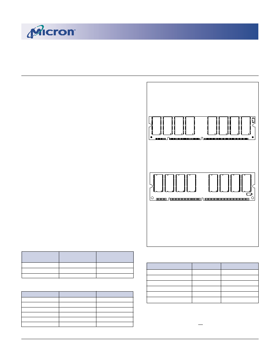
- 168-Pin DIMMs, Low Profile and Standard
- Part Numbers
- General Description
- Serial Presence-Detect Operation
- Pin Assignment
- Functional Block Diagrams
- MT8LST1664A (128MB)
- MT16LSDT3264A (256MB)
- Pin Descriptions
- SDRAM Component Description
- Module Functional Description
- Initialization
- Register Definition
- Mode Register
- Burst Length
- Burst Type
- CAS Latency
- Operating Mode
- Write Burst Mode
- Mode Register Definition Diagram
- Burst Definition Table
- CAS Latency Diagram
- CAS Latency Table
- Commands
- Truth Table - SDRAM Commands and DQMB Operation
- Absolute Maximum Ratings
- DC Electrical Characteristics and Operating Conditions - 128MB Module
- DC Electrical Characteristics and Operating Conditions - 256MB Module
- IDD Specifications and Conditions - 128MB Module
- IDD Specifications and Conditions - 256MB Module
- Capacitance (128MB)
- Capacitance (256MB)
- Electrical Characteristics and Recommended AC Operating Conditions
- AC Functional Characteristics
- Notes
- SPD Clock and Data Conventions
- SPD Start Condition
- SPD Acknowledge
- Figure 1 Data Validity
- Figure 2 Definition of Start and Stop
- Figure 3 Acknowledge Response from Receiver
- EEPROM Device Select Code
- EEPROM Operating Modes
- SPD EEPROM Diagram
- Serial Presence-Detect EEPROM Timing Parameters
- Serial Presence-Detect EEPROM DC Operating Conditions
- Serial Presence-Detect EEPROM AC Operating Conditions
- Serial Presence-Detect Matrix
- 128MB Modules, Low Profile & Standard
- 256MB Module, Low Profile
- 256MB Module, Standard
1
16, 32 Meg x 64 SDRAM DIMMs
©2001, Micron Technology, Inc.
SD8_16C16_32X64AG_C.p65 ≠ Rev. C, Pub. 9/01
128MB / 256MB (x64)
168-PIN SDRAM DIMMs
DEVICE TIMING
Module
PC100
PC133
Markings
CL -
t
RCD -
t
RP
CL -
t
RCD -
t
RP
-13E
2 - 2 - 2
2 - 2 - 2
-133
2 - 2 - 2
3 - 3 - 3
-10E
2 - 2 - 2
NA
SYNCHRONOUS
DRAM MODULE
MT8LSDT1664A - 128MB
MT16LSDT3264A - 256MB
For the latest data sheet, please refer to the Micron Web
site:
www.micron.com/datasheets
FEATURES
∑ PC100- and PC133-compliant
∑ JEDEC-standard 168-pin, dual in-line memory
module (DIMM)
∑ Utilizes 125 MHz and 133 MHz SDRAM compo-
nents
∑ Unbuffered
∑ 128MB (16 Meg x 64)
∑ 256MB (32 Meg x 64)
∑ Single +3.3V ±0.3V power supply
∑ Fully synchronous; all signals registered on
positive edge of system clock
∑ Internal pipelined operation; column address can
be changed every clock cycle
∑ Internal SDRAM banks for hiding row access/
precharge
∑ Programmable burst lengths: 1, 2, 4, 8, or full page
∑ Auto Precharge and Auto Refresh Modes
∑ Self Refresh Mode
∑ 64ms, 4,096-cycle refresh
∑ LVTTL-compatible inputs and outputs
∑ Serial Presence-Detect (SPD)
OPTIONS
MARKING
∑ Package
168-pin DIMM (gold)
G
∑ Frequency/CAS Latency
133 MHz/CL = 2
-13E
133 MHz/CL = 3
-133
100 MHz/CL = 2
-10E
MO168
ADDRESS TABLE
128MB Module
256MB Module
Refresh Count
4K
4K
Device Banks
4 (BA0, BA1)
4 (BA0, BA1)
Device Configuration
16 Meg x 8
16 Meg x 8
Row Addressing
4K (A0≠A11)
4K (A0≠A11)
Column Addressing
1K (A0≠A9)
1K (A0≠A9)
Module Banks
1 (S0,S2)
2 (S0,S2; S1,S3)
PART NUMBERS
PART NUMBER
CONFIGURATION SYSTEM BUS SPEED
MT8LSDT1664AG-13E_
16 Meg x 64
133 MHz
MT8LSDT1664AG-133_
16 Meg x 64
133 MHz
MT8LSDT1664AG-10E_
16 Meg x 64
100 MHz
MT16LSDT3264AG-13E_
32 Meg x 64
133 MHz
MT16LSDT3264AG-133_
32 Meg x 64
133 MHz
MT16LSDT3264AG-10E_
32 Meg x 64
100 MHz
NOTE: The designators for component and PCB revision are the
last two characters of each part number Consult
factory for current revision codes. Example:
MT16LSDT3264AG-133B1.
168-Pin DIMM
Standard
168-Pin DIMM
Low Profile

2
16, 32 Meg x 64 SDRAM DIMMs
©2001, Micron Technology, Inc.
SD8_16C16_32X64AG_C.p65 ≠ Rev. C, Pub. 9/01
128MB / 256MB (x64)
168-PIN SDRAM DIMMs
GENERAL DESCRIPTION
The MT8LSDT1664A and MT16LSDT3264A are
high-speed CMOS, dynamic random-access, 128MB
and 256MB memory modules organized in a x64 con-
figuration. These modules use internally configured
quad-bank SDRAMs with a synchronous interface (all
signals are registered on the positive edge of the clock
signals CK0-CK3).
Read and write accesses to the SDRAM modules are
burst oriented; accesses start at a selected location and
continue for a programmed number of locations in a
programmed sequence. Accesses begin with the regis-
tration of an ACTIVE command, which is then followed
by a READ or WRITE command. The address bits regis-
tered coincident with the ACTIVE command are used
to select the device bank and row to be accessed (BA0,
BA1 select the device bank, A0-A11 select the device
row). The address bits registered coincident with the
READ or WRITE command are used to select the start-
ing column location for the burst access.
The modules provide for programmable READ or
WRITE burst lengths of 1, 2, 4, or 8 locations, or the full
page, with a burst terminate option. An AUTO
PRECHARGE function may be enabled to provide a
self-timed row precharge that is initiated at the end of
the burst sequence.
The modules use an internal pipelined architec-
ture to achieve high-speed operation. This architec-
ture is compatible with the 2n rule of prefetch architec-
tures, but it also allows the column address to be
changed on every clock cycle to achieve a high-speed,
fully random access. Precharging one device bank while
accessing one of the other three device banks will hide
the precharge cycles and provide seamless, high-
speed, random-access operation.
The modules are designed to operate in 3.3V, low-
power memory systems. An auto refresh mode is pro-
vided, along with a power-saving, power-down mode.
All inputs and outputs are LVTTL-compatible.
SDRAM modules offer substantial advances in
DRAM operating performance, including the ability to
synchronously burst data at a high data rate with auto-
matic column-address generation, the ability to inter-
leave between internal banks in order to hide precharge
time and the capability to randomly change column
addresses on each clock cycle during a burst access. For
more information regarding SDRAM operation, refer to
the 128Mb SDRAM data sheet.
SERIAL PRESENCE-DETECT OPERATION
These modules incorporate serial presence-detect
(SPD). The SPD function is implemented using a 2,048-
bit EEPROM. This nonvolatile storage device contains
256 bytes. The first 128 bytes can be programmed by
Micron to identify the module type and various SDRAM
organizations and timing parameters. The remaining
128 bytes of storage are available for use by the cus-
tomer. System READ/WRITE operations between the
master (system logic) and the slave EEPROM device
(DIMM) occur via a standard IIC bus using the DIMM's
SCL (clock) and SDA (data) signals, together with
SA(2:0), which provide eight unique DIMM/EEPROM
addresses.
PIN SYMBOL PIN SYMBOL
PIN
SYMBOL
PIN
SYMBOL
1
V
SS
22
NC
43
V
SS
64
V
SS
2
DQ0
23
V
SS
44
NC
65
DQ21
3
DQ1
24
NC
45
S2#
66
DQ22
4
DQ2
25
NC
46
DQMB2
67
DQ23
5
DQ3
26
V
DD
47
DQMB3
68
V
SS
6
V
DD
27
WE#
48
NC
69
DQ24
7
DQ4
28
DQMB0
49
V
DD
70
DQ25
8
DQ5
29
DQMB1
50
NC
71
DQ26
9
DQ6
30
S0#
51
NC
72
DQ27
10
DQ7
31
NC
52
NC
73
V
DD
11
DQ8
32
V
SS
53
NC
74
DQ28
12
V
SS
33
A0
54
V
SS
75
DQ29
13
DQ9
34
A2
55
DQ16
76
DQ30
14
DQ10
35
A4
56
DQ17
77
DQ31
15
DQ11
36
A6
57
DQ18
78
V
SS
16
DQ12
37
A8
58
DQ19
79
CK2
17
DQ13
38
A10
59
V
DD
80
NC
18
V
DD
39
BA1
60
DQ20
81
WP
19
DQ14
40
V
DD
61
NC
82
SDA
20
DQ15
41
V
DD
62
NC
83
SCL
21
NC
42
CKO
63
CKE1
84
V
DD
PIN ASSIGNMENT (168-PIN DIMM FRONT)
PIN SYMBOL PIN SYMBOL
PIN
SYMBOL
PIN
SYMBOL
85
V
SS
106
NC
127
V
SS
148
V
SS
86
DQ32
107
V
SS
128
CKE0
149
DQ53
87
DQ33
108
NC
129
S3#
150
DQ54
88
DQ34
109
NC
130
DQMB6
151
DQ55
89
DQ35
110
V
DD
131
DQMB7
152
V
SS
90
V
DD
111
CAS#
132
NC
153
DQ56
91
DQ36
112 DQMB4
133
V
DD
154
DQ57
92
DQ37
113 DQMB5
134
NC
155
DQ58
93
DQ38
114
S1#
135
NC
156
DQ59
94
DQ39
115
RAS#
136
NC
157
V
DD
95
DQ40
116
V
SS
137
NC
158
DQ60
96
V
SS
117
A1
138
V
SS
159
DQ61
97
DQ41
118
A3
139
DQ48
160
DQ62
98
DQ42
119
A5
140
DQ49
161
DQ63
99
DQ43
120
A7
141
DQ50
162
V
SS
100
DQ44
121
A9
142
DQ51
163
CK3
101
DQ45
122
BA0
143
V
DD
164
NC
102
V
DD
123
A11
144
DQ52
165
SA0
103
DQ46
124
V
DD
145
NC
166
SA1
104
DQ47
125
CK1
146
NC
167
SA2
105
NC
126
NC
147
NC
168
V
DD
PIN ASSIGNMENT (168-Pin DIMM BACK)
3
16, 32 Meg x 64 SDRAM DIMMs
©2001, Micron Technology, Inc.
SD8_16C16_32X64AG_C.p65 ≠ Rev. C, Pub. 9/01
128MB / 256MB (x64)
168-PIN SDRAM DIMMs
FUNCTIONAL BLOCK DIAGRAM
MT8LSDT1664A (128MB)
NOTE: 1. All resistor values are 10 ohms unless otherwise specified.
2. Reference designators in this diagram do not necessarily match the actual module.
DQM CS#
U8
U1-U4/U6-U9 = MT48LC16M8A2TG SDRAMs
A0
SA0
SPD
SDA
A1
SA1
A2
SA2
DQ0
DQ1
DQ2
DQ3
DQ4
DQ5
DQ6
DQ7
DQ56
DQ57
DQ58
DQ59
DQ60
DQ61
DQ62
DQ63
DQMB7
DQM CS#
U6
DQ0
DQ1
DQ2
DQ3
DQ4
DQ5
DQ6
DQ7
DQ48
DQ49
DQ50
DQ51
DQ52
DQ53
DQ54
DQ55
DQMB6
DQM CS#
U4
DQ0
DQ1
DQ2
DQ3
DQ4
DQ5
DQ6
DQ7
DQ40
DQ41
DQ42
DQ43
DQ44
DQ45
DQ46
DQ47
DQMB5
DQM CS#
U2
DQ0
DQ1
DQ2
DQ3
DQ4
DQ5
DQ6
DQ7
DQ32
DQ33
DQ34
DQ35
DQ36
DQ37
DQ38
DQ39
DQMB4
DQM CS#
U9
DQ0
DQ1
DQ2
DQ3
DQ4
DQ5
DQ6
DQ7
DQ24
DQ25
DQ26
DQ27
DQ28
DQ29
DQ30
DQ31
DQMB3
DQM CS#
U7
DQ0
DQ1
DQ2
DQ3
DQ4
DQ5
DQ6
DQ7
DQ16
DQ17
DQ18
DQ19
DQ20
DQ21
DQ22
DQ23
DQMB2
DQM CS#
U3
DQ0
DQ1
DQ2
DQ3
DQ4
DQ5
DQ6
DQ7
DQ8
DQ9
DQ10
DQ11
DQ12
DQ13
DQ14
DQ15
DQMB1
DQM CS#
U1
DQ0
DQ1
DQ2
DQ3
DQ4
DQ5
DQ6
DQ7
DQ0
DQ1
DQ2
DQ3
DQ4
DQ5
DQ6
DQ7
DQMB0
S2#
S0#
RAS#
CAS#
CKE0
WE#
RAS#: SDRAMs U1-U4/U6-U9
CAS#: SDRAMs U1-U4/U6-U9
CKE0: SDRAMs U1-U4/U6-U9
WE#: SDRAMs U1-U4/U6-U9
A0-A11: SDRAMs U1-U4/U6-U9
BA0: SDRAMs U1-U4/U6-U9
BA1: SDRAMs U1-U4/U6-U9
A0-A11
BA0
BA1
V
DD
V
SS
SDRAMs U1-U4/U6-U9
SDRAMs U1-U4/U6-U9
10pF
CK1, CK3
U1
U2
U3
U4
CK0
U6
U7
U8
CK2
3.3pF
3.3pF
SCL
WP
2.2
µ
F
2.2
µ
F
U9
U10

4
16, 32 Meg x 64 SDRAM DIMMs
©2001, Micron Technology, Inc.
SD8_16C16_32X64AG_C.p65 ≠ Rev. C, Pub. 9/01
128MB / 256MB (x64)
168-PIN SDRAM DIMMs
FUNCTIONAL BLOCK DIAGRAM
MT16LSDT3264A (256MB)
NOTE: 1. All resistor values are 10 ohms unless otherwise specified.
2. Reference designators in this diagram do not necessarily match the actual module.
DQM CS#
U8
U1-U4; U6-U9; U11-U14; U16-U19 = MT48LC16M8A2TG SDRAMs
A0
SA0
SPD
SDA
A1
SA1
A2
SA2
DQ0
DQ1
DQ2
DQ3
DQ4
DQ5
DQ6
DQ7
DQ56
DQ57
DQ58
DQ59
DQ60
DQ61
DQ62
DQ63
DQMB7
DQM CS#
U6
DQ0
DQ1
DQ2
DQ3
DQ4
DQ5
DQ6
DQ7
DQ48
DQ49
DQ50
DQ51
DQ52
DQ53
DQ54
DQ55
DQMB6
DQM CS#
U4
DQ0
DQ1
DQ2
DQ3
DQ4
DQ5
DQ6
DQ7
DQ40
DQ41
DQ42
DQ43
DQ44
DQ45
DQ46
DQ47
DQMB5
DQM CS#
U2
DQ0
DQ1
DQ2
DQ3
DQ4
DQ5
DQ6
DQ7
DQ32
DQ33
DQ34
DQ35
DQ36
DQ37
DQ38
DQ39
DQMB4
DQM CS#
U9
DQ0
DQ1
DQ2
DQ3
DQ4
DQ5
DQ6
DQ7
DQ24
DQ25
DQ26
DQ27
DQ28
DQ29
DQ30
DQ31
DQMB3
DQM CS#
U7
DQ0
DQ1
DQ2
DQ3
DQ4
DQ5
DQ6
DQ7
DQ16
DQ17
DQ18
DQ19
DQ20
DQ21
DQ22
DQ23
DQMB2
DQM CS#
U3
DQ0
DQ1
DQ2
DQ3
DQ4
DQ5
DQ6
DQ7
DQ8
DQ9
DQ10
DQ11
DQ12
DQ13
DQ14
DQ15
DQMB1
DQM CS#
U1
DQ0
DQ1
DQ2
DQ3
DQ4
DQ5
DQ6
DQ7
DQ0
DQ1
DQ2
DQ3
DQ4
DQ5
DQ6
DQ7
DQMB0
S2#
S0#
CKE1
CKE0
CAS#
RAS#
WE#
CKE: SDRAMs U11-U14; U16-U19
CKE: SDRAMs U1-U4; U6-U9
CAS#: SDRAMs U1-U4; U6-U9; U11-U14; U16-U19
RAS#: SDRAMs U1-U4; U6-U9; U11-U14; U16-U19
WE#: SDRAMs U1-U4; U6-U9; U11-U14; U16-U19
A0-A11: SDRAMs U1-U4; U6-U9; U11-U14; U16-U19
BA0: SDRAMs U1-U4; U6-U9; U11-U14; U16-U19
BA1: SDRAMs U1-U4; U6-U9; U11-U14; U16-U19
A0-A11
BA0
BA1
V
DD
V
SS
SDRAMs U1-U4; U6-U9; U11-U14; U16-U19
SDRAMs U1-U4; U6-U9; U11-U14; U16-U19
DQM CS#
U12
DQ0
DQ1
DQ2
DQ3
DQ4
DQ5
DQ6
DQ7
DQM CS#
U14
DQ0
DQ1
DQ2
DQ3
DQ4
DQ5
DQ6
DQ7
DQM CS#
U16
DQ0
DQ1
DQ2
DQ3
DQ4
DQ5
DQ6
DQ7
DQM CS#
U18
DQ0
DQ1
DQ2
DQ3
DQ4
DQ5
DQ6
DQ7
S1#
DQM CS#
U11
DQ0
DQ1
DQ2
DQ3
DQ4
DQ5
DQ6
DQ7
DQM CS#
U13
DQ0
DQ1
DQ2
DQ3
DQ4
DQ5
DQ6
DQ7
DQM CS#
U17
DQ0
DQ1
DQ2
DQ3
DQ4
DQ5
DQ6
DQ7
DQM CS#
U19
DQ0
DQ1
DQ2
DQ3
DQ4
DQ5
DQ6
DQ7
S3#
V
DD
10K
U1
U2
CK0
U16
U17
U18
U19
CK1
U6
U7
U8
U9
CK2
3.3pF
U11
U12
U13
U14
CK3
3.3pF
SCL
WP
2.2
µ
F
2.2
µ
F
U3
U4
U10
5
16, 32 Meg x 64 SDRAM DIMMs
©2001, Micron Technology, Inc.
SD8_16C16_32X64AG_C.p65 ≠ Rev. C, Pub. 9/01
128MB / 256MB (x64)
168-PIN SDRAM DIMMs
PIN DESCRIPTIONS*
PIN NUMBERS
SYMBOL
TYPE
DESCRIPTION
27, 115, 111
RAS#, CAS#,
Input
Command Inputs: RAS#, CAS#, and WE# (along with
WE#
S0#-S3#) define the command being entered.
42, 79, 125, 163
CK0-CK3
Input
Clock: CK0-CK3 are driven by the system clock. All
SDRAM input signals are sampled on the positive
edge of CK. CK also increments the internal burst
counter and controls the output registers.
63, 128
CKE0, CKE1
Input
Clock Enable: CKE0-CKE1 activate (HIGH) and
deactivate (LOW) the CK0-CK3 signals. Deactivating
the clock provides PRECHARGE POWER-DOWN and
SELF REFRESH operation (all device banks idle),
ACTIVE POWER-DOWN (row ACTIVE in any device
bank) or CLOCK SUSPEND operation (burst access in
progress). CKE0-CKE1 are synchronous except after the
device enters power-down and self refresh modes,
where CKE0-CKE1 become asynchronous until after
exiting the same mode. The input buffers, including
CK0-CK3, are disabled during power-down and self
refresh modes, providing low standby power.
30, 45, 114, 129
S0#-S3#
Input
Chip Select: S0#-S3# enable (registered LOW) and
disable (registered HIGH) the command decoder. All
commands are masked when S0#-S3# are registered
HIGH. S0#-S3# are considered part of the command
code.
28-29, 46-47,
DQMB0-DQMB7
Input
Input/Output Mask: DQMB is an input mask signal for
112-113, 130-131
write accesses and an output enable signal for read
accesses. Input data is masked when DQMB is sampled
HIGH during a WRITE cycle. The output buffers are
placed in a High-Z state (two-clock latency) when
DQMB is sampled HIGH during a READ cycle.**
39, 122
BA0, BA1
Input
Bank Address: BA0 and BA1 define to which device
bank the ACTIVE, READ, WRITE, or PRECHARGE
command is being applied.
33, 34, 35, 36, 37, 38,
A0-A11
Input
Address Inputs: A0-A11 are sampled during the
117, 118, 119, 120, 121,
ACTIVE command (row-address A0-A11) and
123
READ/WRITE command (column-address A0-A9, with
A10 defining auto precharge) to select one location
out of the memory array in the respective device bank.
A10 is sampled during a PRECHARGE command to
determine if all device banks are to be precharged
(A10 HIGH) or device bank selected by BA0, BA1
(LOW). The address inputs also provide the op-code
during a LOAD MODE REGISTER command.
81
WP
Input
Write Protect: Serial presence-detect hardware write
protect.
83
SCL
Input
Serial Clock for Presence-Detect: SCL is used to
synchronize the presence-detect data transfer to and
from the module.
*Pin numbers do not necessarily correlate with symbols.
**Pin numbers listed in module pinout order.