 | –≠–ª–µ–∫—Ç—Ä–æ–Ω–Ω—ã–π –∫–æ–º–ø–æ–Ω–µ–Ω—Ç: MT18D836X | –°–∫–∞—á–∞—Ç—å:  PDF PDF  ZIP ZIP |
Document Outline
- Features
- Options
- Key Timing Parameters
- Part Numbers
- General Description
- Pin Assignment (Front View)
- EDO Page Mode
- Refresh
- JEDEC-Defined Presence-Detect - MT9D436 (16MB)
- JEDEC-Defined Presence-Detect - MT18D836 (32MB)
- Functional Block Diagrams
- MT9D436 (16MB)
- MT18D836 (32MB)
- Absolute Maximum Ratings
- DC Electrical Characteristics and Operating Conditions
- ICC Specifications and Conditions
- Capacitance
- AC Electrical Characteristics
- AC Electrical Characteristics
- Notes
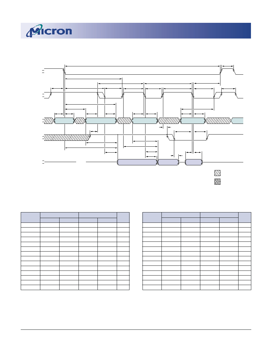
- Read Cycle
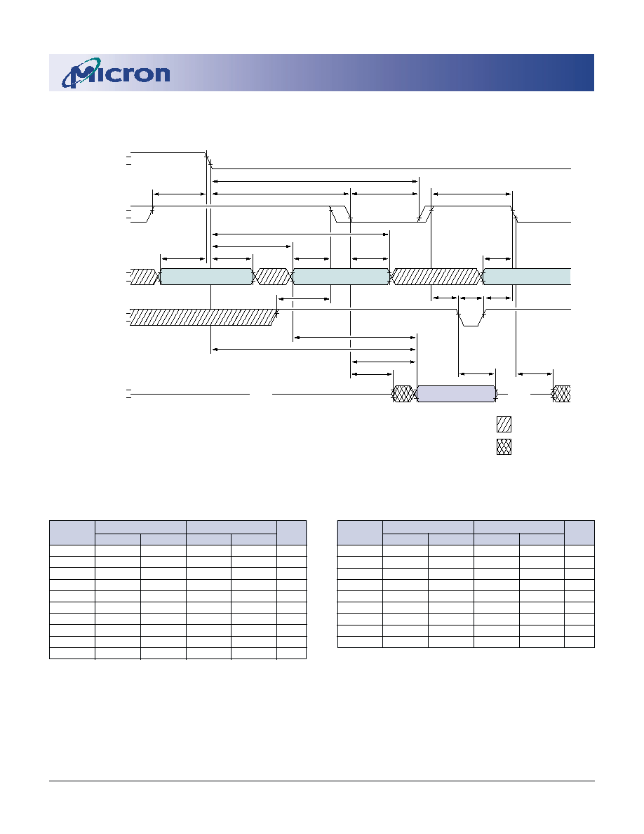
- Early Write Cycle
- EDO-Page-Mode Read Cycle
- EDO-Page-Mode Early-Write Cycle
- EDO Page-Mode Read-Early-Write Cycle
- EDO Read Cycle
- RAS#-Only Refresh Cycle
- CBR Refresh Cycle
- Hidden Refresh Cycle
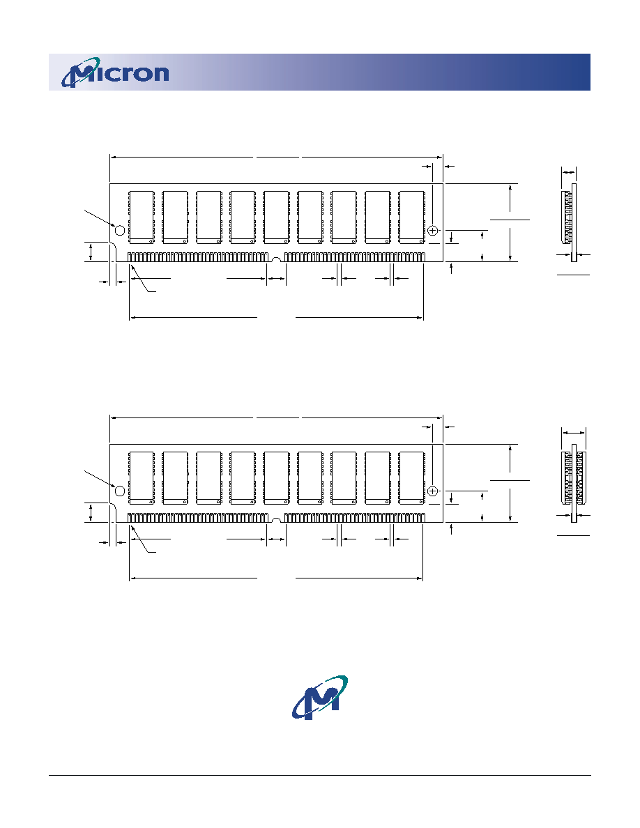
- 72-Pin SIMM (16MB)
- 72-Pin SIMM (32MB)
4, 8 Meg x 36 ECC-Optimized DRAM SIMMs
Micron Technology, Inc., reserves the right to change products or specifications without notice.
DM65_2.p65 ≠ Rev. 9/98
©1998, Micron Technology, Inc.
1
4, 8 MEG x 36
ECC-OPTIMIZED DRAM SIMMs
NOT RECOMMENDED FOR NEW DESIGNS
DRAM
MODULE
MT9D436 X
MT18D836 X
For the latest data sheet revisions, please refer to the
Micron Web site:
www.micron.com/datasheets
FEATURES
∑ Four-CAS#, ECC-optimized configuration in a 72-
pin, single in-line memory module (SIMM)
∑ 16MB (4 Meg x 36) and 32MB (8 Meg x 36)
∑ High-performance CMOS silicon-gate process
∑ Single 5V ±10% power supply
∑ All inputs, outputs and clocks are TTL-compatible
∑ Refresh modes: RAS#-ONLY, CAS#-BEFORE-RAS#
(CBR) and HIDDEN
∑ 2,048-cycle refresh distributed across 32ms
∑ Extended Data-Out (EDO) PAGE MODE access
OPTIONS
MARKING
∑ Timing
50ns access
-5
60ns access
-6
∑ Package
72-pin SIMM
M
GENERAL DESCRIPTION
The MT9D436 X and MT18D836 X are randomly
accessed, 16MB and 32MB solid-state memories orga-
nized in a x36 configuration. These modules are de-
signed for systems that utilize ECC and do not conduct
single-byte accesses. These modules do not support
parity functionality.
During READ or WRITE cycles, each bit is uniquely
addressed through 20 address bits that are entered 10
bits (A0-A9) at a time. RAS# is used to latch the first 10
bits and CAS# the latter 10 bits. READ or WRITE cycles
are selected with the WE# input. A logic HIGH on WE#
dictates read mode, while a logic LOW on WE# dictates
write mode. During a WRITE cycle, data-in (D) is latched
by the falling edge of WE# or CAS#, whichever occurs
last. EARLY WRITE occurs when WE# goes LOW prior to
CAS# going LOW, and the output pin(s) remain open
(High-Z) until the next CAS# cycle.
EDO PAGE MODE
EDO PAGE MODE is an accelerated FAST-PAGE-
MODE cycle. The primary advantage of EDO is the
availability of data-out even after CAS# goes back HIGH.
EDO provides for CAS# precharge time (
t
CP) to occur
without the output data going invalid. This elimina-
tion of CAS# output control provides for pipelined
READs.
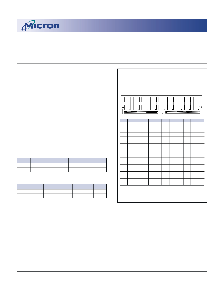
PIN ASSIGNMENT (Front View)
72-Pin SIMM
4 Meg x 36 (shown)
8 Meg x 36
PIN SYMBOL
PIN SYMBOL
PIN SYMBOL
PIN SYMBOL
1
V
SS
19
A10
37
DQ18
55
DQ13
2
DQ1
20
DQ5
38
DQ36
56
DQ31
3
DQ19
21
DQ23
39
V
SS
57
DQ14
4
DQ2
22
DQ6
40
CAS0#
58
DQ32
5
DQ20
23
DQ24
41
CAS2#
59
V
DD
6
DQ3
24
DQ7
42
CAS3#
60
DQ33
7
DQ21
25
DQ25
43
CAS1#
61
DQ15
8
DQ4
26
DQ8
44
RAS0#
62
DQ34
9
DQ22
27
DQ26
45 NC/RAS1#* 63
DQ16
10
V
DD
28
A7
46
NC
64
DQ35
11
NC
29
NC (A11)
47
WE#
65
DQ17
12
A0
30
V
DD
48
NC
66
NC
13
A1
31
A8
49
DQ10
67
PRD1
14
A2
32
A9
50
DQ28
68
PRD2
15
A3
33 NC/RAS3#* 51
DQ11
69
PRD3
16
A4
34
RAS2#
52
DQ29
70
PRD4
17
A5
35
DQ27
53
DQ12
71
NC
18
A6
36
DQ9
54
DQ30
72
V
SS
*32MB version only
NOTE: Symbols in parentheses are not used on these
modules but may be used for other modules in this
product family. They are for reference only.
1
36
37
72
PART NUMBERS
PART NUMBER
CONFIGURATION
FEATURES
MODE
MT9D436M-x X
4 Meg x 36
4 CAS#, ECC
EDO
MT18D836M-x X
8 Meg x 36
4 CAS#, ECC
EDO
x = speed
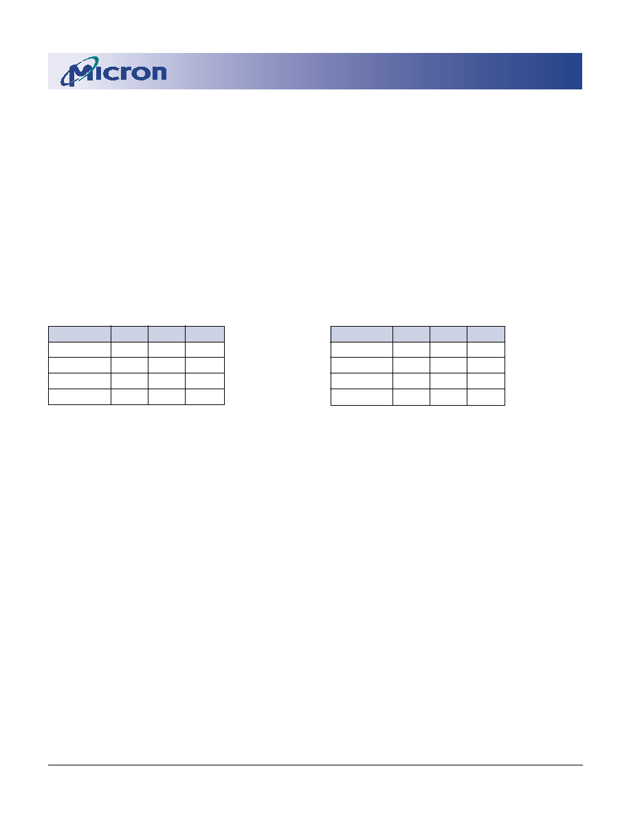
KEY TIMING PARAMETERS
SPEED
t
RC
t
RAC
t
PC
t
AA
t
CAC
t
CAS
-5
84ns
50ns
20ns
25ns
13ns
8ns
-6
104ns
60ns
25ns
30ns
15ns
10ns
4, 8 Meg x 36 ECC-Optimized DRAM SIMMs
Micron Technology, Inc., reserves the right to change products or specifications without notice.
DM65_2.p65 ≠ Rev. 9/98
©1998, Micron Technology, Inc.
2
4, 8 MEG x 36
ECC-OPTIMIZED DRAM SIMMs
NOT RECOMMENDED FOR NEW DESIGNS
REFRESH
Returning RAS# and CAS# HIGH terminates a
memory cycle and decreases chip current to a reduced
standby level. Also, the chip is preconditioned for the
next cycle during the RAS# HIGH time. Memory cell
data is retained in its correct state by maintaining
power and executing anyRAS# cycle (READ, WRITE) or
RAS# REFRESH cycle (RAS# ONLY, CBR or HIDDEN) so
that all 2,048 combinations of RAS# addresses are ex-
ecuted at least every 32ms, regardless of sequence.
The CBR REFRESH cycle will invoke the refresh counter
for automatic RAS# addressing.
FAST-PAGE-MODE modules have traditionally
turned the output buffers off (High-Z) with the rising
edge of CAS#. EDO operates like FAST-PAGE-MODE
READs, except data will be held valid or become valid
after CAS# goes HIGH, as long as RAS# is held LOW.
(Refer to the MT4C4M4E8 DRAM data sheet for addi-
tional information on EDO functionality.)
EDO PAGE MODE (continued)
JEDEC-DEFINED
PRESENCE-DETECT ≠ MT18D836 (32MB)
SYMBOL
PIN
-5
-6
PRD1
67
NC
NC
PRD2
68
Vss
Vss
PRD3
69
Vss
NC
PRD4
70
Vss
NC
JEDEC-DEFINED
PRESENCE-DETECT ≠ MT9D436 (16MB)
SYMBOL
PIN
-5
-6
PRD1
67
Vss
Vss
PRD2
68
NC
NC
PRD3
69
Vss
NC
PRD4
70
Vss
NC

4, 8 Meg x 36 ECC-Optimized DRAM SIMMs
Micron Technology, Inc., reserves the right to change products or specifications without notice.
DM65_2.p65 ≠ Rev. 9/98
©1998, Micron Technology, Inc.
3
4, 8 MEG x 36
ECC-OPTIMIZED DRAM SIMMs
NOT RECOMMENDED FOR NEW DESIGNS
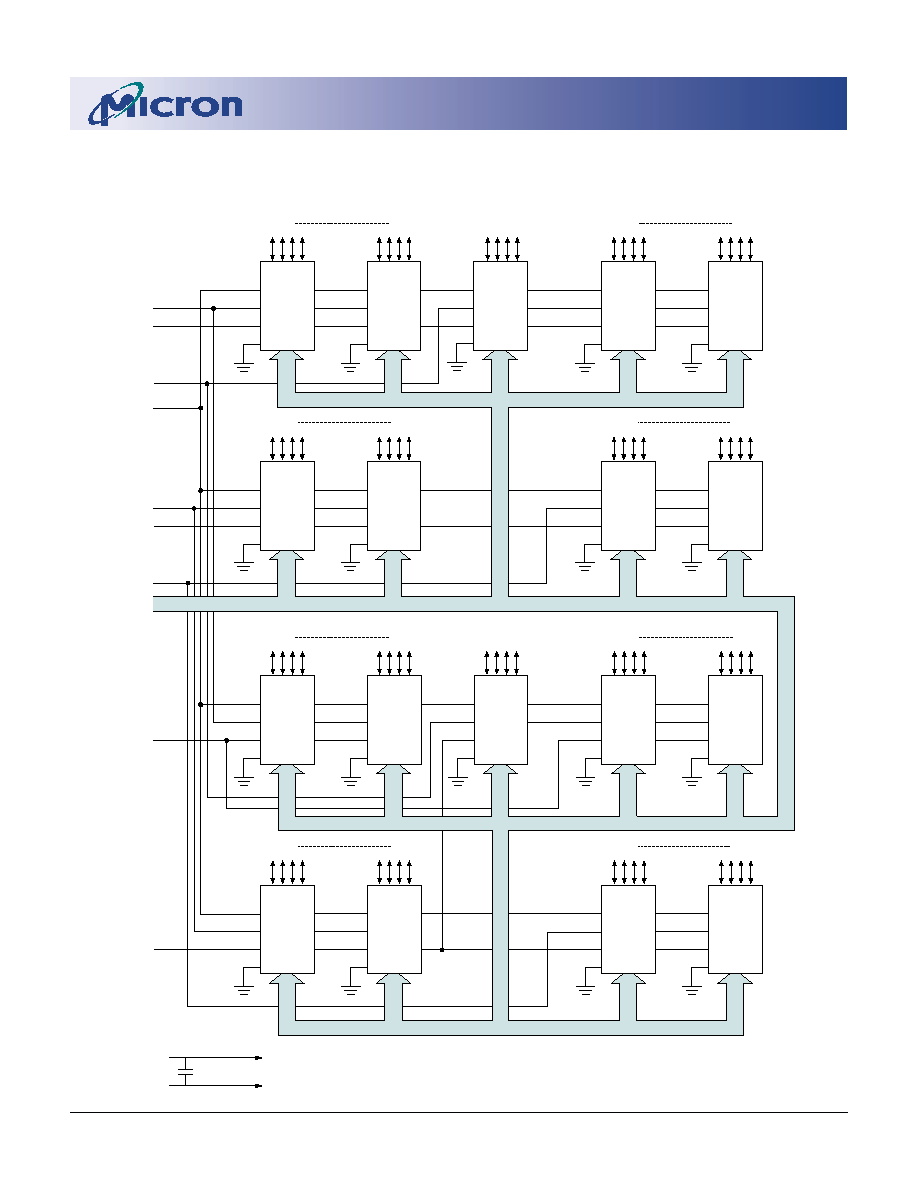
FUNCTIONAL BLOCK DIAGRAM
MT9D436 (16MB)
DQ1
DQ9, 18, 27, 36
DQ10
DQ17
CAS1#
WE#
DQ19
DQ26
DQ28
DQ35
CAS3#
A0≠A10
11
11
11
11
11
11
11
11
11
U1-U9 = 4 Meg x 4 DRAMs
DQ8
CAS0#
RAS0#
CAS2#
RAS2#
WE#
CAS#
RAS#
OE#
DQ1 - 4
U1
A0≠A10
WE#
CAS#
RAS#
OE#
DQ1 - 4
U2
WE#
CAS#
RAS#
OE#
DQ1 - 4
U5
WE#
CAS#
RAS#
OE#
DQ1 - 4
U3
WE#
CAS#
RAS#
OE#
DQ1 - 4
WE#
CAS#
RAS#
OE#
DQ1 - 4
WE#
CAS#
RAS#
OE#
DQ1 - 4
WE#
CAS#
RAS#
OE#
DQ1 - 4
U3
WE#
CAS#
RAS#
OE#
DQ1 - 4
U4
U6
U7
U8
U9
V
DD
V
SS
U1-U9
U1-U9
A0≠A10
A0≠A10
A0≠A10
A0≠A10
A0≠A10
A0≠A10
A0≠A10
A0≠A10
4, 8 Meg x 36 ECC-Optimized DRAM SIMMs
Micron Technology, Inc., reserves the right to change products or specifications without notice.
DM65_2.p65 ≠ Rev. 9/98
©1998, Micron Technology, Inc.
4
4, 8 MEG x 36
ECC-OPTIMIZED DRAM SIMMs
NOT RECOMMENDED FOR NEW DESIGNS
FUNCTIONAL BLOCK DIAGRAM
MT18D836 (32MB)
DQ1
DQ9, 18, 27, 36
DQ10
DQ17
CAS1#
WE#
DQ19
DQ26
DQ28
DQ35
CAS3#
A0≠A10
11
11
11
11
11
11
11
11
11
U1-U18 = 4 Meg x 4 DRAMs
DQ1
DQ9, 18, 27, 36
DQ10
DQ17
RAS1#
DQ19
DQ26
DQ28
DQ35
11
11
11
11
11
11
11
11
11
DQ8
DQ8
CAS0#
RAS0#
CAS2#
RAS3#
RAS2#
WE#
CAS#
RAS#
OE#
DQ1 - 4
WE#
CAS#
RAS#
OE#
DQ1 - 4
WE#
CAS#
RAS#
OE#
DQ1 - 4
WE#
CAS#
RAS#
OE#
DQ1 - 4
WE#
CAS#
RAS#
OE#
DQ1 - 4
WE#
CAS#
RAS#
OE#
DQ1 - 4
WE#
CAS#
RAS#
OE#
DQ1 - 4
WE#
CAS#
RAS#
OE#
DQ1 - 4
WE#
CAS#
RAS#
OE#
DQ1 - 4
U1
U2
U5
U6
U7
U3
U4
U8
U9
WE#
CAS#
RAS#
OE#
DQ1 - 4
WE#
CAS#
RAS#
OE#
DQ1 - 4
WE#
CAS#
RAS#
OE#
DQ1 - 4
WE#
CAS#
RAS#
OE#
DQ1 - 4
WE#
CAS#
RAS#
OE#
DQ1 - 4
WE#
CAS#
RAS#
OE#
DQ1 - 4
WE#
CAS#
RAS#
OE#
DQ1 - 4
WE#
CAS#
RAS#
OE#
DQ1 - 4
WE#
CAS#
RAS#
OE#
DQ1 - 4
U10
U11
U14
U15
U16
U12
U13
U17
U18
A0≠A10
A0≠A10
A0≠A10
A0≠A10
A0≠A10
A0≠A10
A0≠A10
A0≠A10
A0≠A10
A0≠A10
A0≠A10
A0≠A10
A0≠A10
A0≠A10
A0≠A10
A0≠A10
A0≠A10
A0≠A10
V
DD
V
SS
U1-U18
U1-U18

4, 8 Meg x 36 ECC-Optimized DRAM SIMMs
Micron Technology, Inc., reserves the right to change products or specifications without notice.
DM65_2.p65 ≠ Rev. 9/98
©1998, Micron Technology, Inc.
5
4, 8 MEG x 36
ECC-OPTIMIZED DRAM SIMMs
NOT RECOMMENDED FOR NEW DESIGNS
ABSOLUTE MAXIMUM RATINGS*
Voltage on V
DD
Supply Relative to V
SS
....... -1V to +7V
Operating Temperature, T
A
(ambient) ... 0∞C to +70∞C
Storage Temperature (plastic) ............ -55∞C to +125∞C
Power Dissipation ................................................... 9W
Short Circuit Output Current ............................. 50mA
*Stresses greater than those listed under "Absolute
Maximum Ratings" may cause permanent damage to
the device. This is a stress rating only, and functional
operation of the device at these or any other conditions
above those indicated in the operational sections of
this specification is not implied. Exposure to absolute
maximum rating conditions for extended periods may
affect reliability.
DC ELECTRICAL CHARACTERISTICS AND OPERATING CONDITIONS
(Notes: 1, 5, 6) (V
DD
= +5V ±10%)
PARAMETER/CONDITION
SYMBOL MIN
MAX
UNITS NOTES
SUPPLY VOLTAGE
V
DD
4.5
5.5
V
INPUT HIGH VOLTAGE: Logic 1; All inputs
V
IH
2.4
V
DD
+ 1
V
INPUT LOW VOLTAGE: Logic 0; All inputs
V
IL
-1.0
0.8
V
INPUT LEAKAGE CURRENT:
CAS0#-CAS3#
I
I
1
-12
12
µA
22
Any input 0V
V
IN
5.5V
A0-A10, WE#
I
I
2
-36
36
µA
22
(All other pins not under test = 0V)
RAS0#-RAS3#
I
I
3
-10
10
µA
OUTPUT LEAKAGE CURRENT:
DQ1-DQ36
I
OZ
-10
10
µA
22
(DQ is disabled; 0V
V
OUT
5.5V)
OUTPUT LEVELS:
V
OH
2.4
≠
V
Output High Voltage (I
OUT
= -5mA)
Output Low Voltage (I
OUT
= 4.2mA)
V
OL
≠
0.4
V
MAX
Icc SPECIFICATIONS AND CONDITIONS
(Notes: 1, 5, 6) (V
DD
= +5V ±10%)
PARAMETER/CONDITION
SYMBOL
SIZE
-5
-6
UNITS NOTES
STANDBY CURRENT: (TTL)
I
CC
1
16MB
9
9
mA
(RAS# = CAS# = V
IH
)
32MB
18
18
STANDBY CURRENT: (CMOS)
I
CC
2
16MB
5
5
mA
(RAS# = CAS# = Other Inputs = V
DD
- 0.2V)
32MB
9
9
OPERATING CURRENT: Random READ/WRITE
16MB
1,260
1,170
mA
3, 21
Average power supply current
I
CC
3
(RAS#, CAS#, address cycling:
t
RC =
t
RC [MIN])
32MB
1,269
1,179
OPERATING CURRENT: EDO PAGE MODE
16MB
990
900
mA
3, 21
Average power supply current
I
CC
4
(RAS# = V
IL
, CAS#, address cycling:
t
PC =
t
PC [MIN])
32MB
999
909
REFRESH CURRENT: RAS#-ONLY
16MB
1,260
1,170
mA
3, 21
Average power supply current
I
CC
5
(RAS# cycling, CAS# = V
IH
:
t
RC =
t
RC [MIN])
32MB
1,269
1,179
REFRESH CURRENT: CBR
16MB
1,260
1,170
mA
3, 4
Average power supply current
I
CC
6
(RAS#, CAS#, address cycling;
t
RC =
t
RC [MIN])
32MB
1,269
1,179
4, 8 Meg x 36 ECC-Optimized DRAM SIMMs
Micron Technology, Inc., reserves the right to change products or specifications without notice.
DM65_2.p65 ≠ Rev. 9/98
©1998, Micron Technology, Inc.
6
4, 8 MEG x 36
ECC-OPTIMIZED DRAM SIMMs
NOT RECOMMENDED FOR NEW DESIGNS
AC ELECTRICAL CHARACTERISTICS
(Notes: 5, 6, 7, 8, 9, 10, 11, 12) (V
DD
= +5V ±10%)
AC CHARACTERISTICS
-5
-6
PARAMETER
SYMBOL
MIN
MAX
MIN
MAX
UNITS
NOTES
Access time from column address
t
AA
25
30
ns
Column-address setup to CAS# precharge during WRITE
t
ACH
12
15
ns
Column-address hold time (referenced to RAS#)
t
AR
38
45
ns
Column-address setup time
t
ASC
0
0
ns
Row-address setup time
t
ASR
0
0
ns
Access time from CAS#
t
CAC
13
15
ns
Column-address hold time
t
CAH
8
10
ns
CAS# pulse width
t
CAS
8
10,000
10
10,000
ns
CAS# hold time (CBR Refresh)
t
CHR
8
10
ns
4
CAS# to output in Low-Z
t
CLZ
0
0
ns
Data output hold after next CAS# LOW
t
COH
3
3
ns
CAS# precharge time
t
CP
8
10
ns
13
Access time from CAS# precharge
t
CPA
28
35
ns
CAS# to RAS# precharge time
t
CRP
5
5
ns
CAS# hold time
t
CSH
38
45
ns
CAS# setup time (CBR Refresh)
t
CSR
5
5
ns
4
WRITE command to CAS# lead time
t
CWL
8
10
ns
Data-in hold time
t
DH
8
10
ns
18
Data-in setup time
t
DS
0
0
ns
18
Output buffer turn-off delay
t
OFF
0
12
0
15
ns
17
EDO-PAGE-MODE READ or WRITE cycle time
t
PC
20
25
ns
Access time from RAS#
t
RAC
50
60
ns
RAS# to column-address delay time
t
RAD
9
12
ns
15
Row-address hold time
t
RAH
9
10
ns
RAS# pulse width
t
RAS
50
10,000
60
10,000
ns
RAS# pulse width (EDO PAGE MODE)
t
RASP
50
125,000
60
125,000
ns
Random READ or WRITE cycle time
t
RC
84
104
ns
RAS# to CAS# delay time
t
RCD
11
14
ns
14
READ command hold time (referenced to CAS#)
t
RCH
0
0
ns
16
READ command setup time
t
RCS
0
0
ns
Refresh period (2,048 cycles)
t
REF
32
32
ms
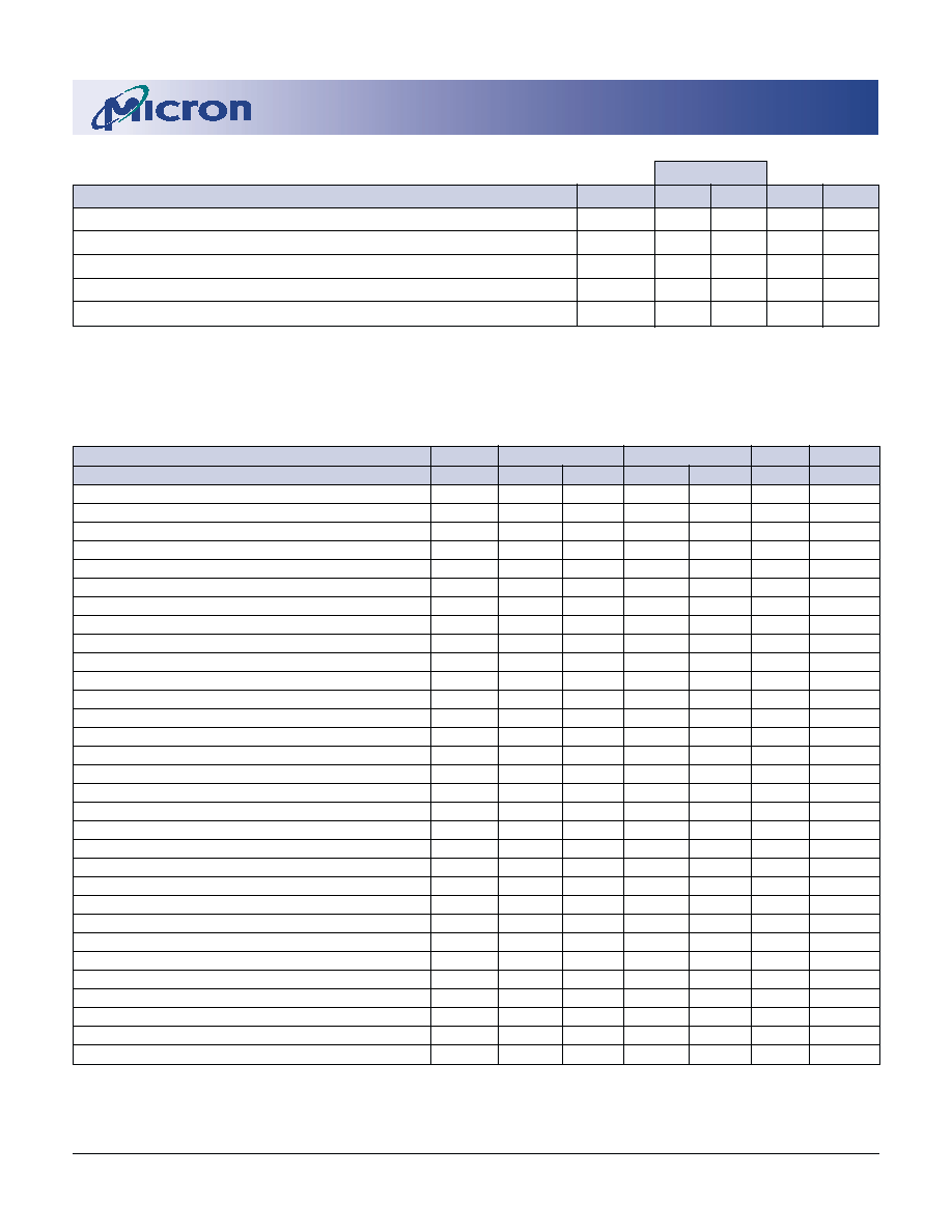
CAPACITANCE
PARAMETER
SYMBOL 16MB
32MB UNITS NOTES
Input Capacitance: A0-A10
C
I
1
52
105
pF
2
Input Capacitance: WE#
C
I
2
70
140
pF
2
Input Capacitance: RAS0#-RAS3#
C
I
3
42
42
pF
2
Input Capacitance: CAS0#-CAS3#
C
I
4
25
50
pF
2
Input/Output Capacitance: DQ1-DQ36
C
IO
10
18
pF
2
MAX
4, 8 Meg x 36 ECC-Optimized DRAM SIMMs
Micron Technology, Inc., reserves the right to change products or specifications without notice.
DM65_2.p65 ≠ Rev. 9/98
©1998, Micron Technology, Inc.
7
4, 8 MEG x 36
ECC-OPTIMIZED DRAM SIMMs
NOT RECOMMENDED FOR NEW DESIGNS
AC ELECTRICAL CHARACTERISTICS
(Notes: 5, 6, 7, 8, 9, 10, 11, 12) (V
DD
= +5V ±10%)
AC CHARACTERISTICS
-5
-6
PARAMETER
SYMBOL
MIN
MAX
MIN
MAX
UNITS
NOTES
RAS# precharge time
t
RP
30
40
ns
RAS# to CAS# precharge time
t
RPC
5
5
ns
READ command hold time (referenced to RAS#)
t
RRH
0
0
ns
16
RAS# hold time
t
RSH
13
15
ns
WRITE command to RAS# lead time
t
RWL
13
15
ns
Transition time (rise or fall)
t
T
2
50
2
50
ns
WRITE command hold time
t
WCH
8
10
ns
WRITE command hold time (referenced to RAS#)
t
WCR
38
45
ns
WE# command setup time
t
WCS
0
0
ns
Output disable delay from WE# (CAS# HIGH)
t
WHZ
0
12
0
15
ns
WRITE command pulse width
t
WP
5
5
ns
WE# pulse width for output disable when CAS# HIGH
t
WPZ
10
10
ns
WE# hold time (CBR Refresh)
t
WRH
8
10
ns
WE# setup time (CBR Refresh)
t
WRP
8
10
ns

4, 8 Meg x 36 ECC-Optimized DRAM SIMMs
Micron Technology, Inc., reserves the right to change products or specifications without notice.
DM65_2.p65 ≠ Rev. 9/98
©1998, Micron Technology, Inc.
8
4, 8 MEG x 36
ECC-OPTIMIZED DRAM SIMMs
NOT RECOMMENDED FOR NEW DESIGNS
NOTES
1. All voltages referenced to V
SS
.
2. This parameter is sampled. Capacitance is
measured using MIL-STD-883C, Method 3012.1 (1
MHz AC,
V
DD
= 4.5V, DC bias = 2.4V at 15mV RMS).
3. I
CC
is dependent on output loading and cycle
rates. Specified values are obtained with mini-
mum cycle time and the outputs open.
4. Enables on-chip refresh and address counters.
5. The minimum specifications are used only to
indicate cycle time at which proper operation over
the full temperature range is ensured.
6. An initial pause of 100µs is required after power-
up, followed by eight RAS# refresh cycles (RAS#-
ONLY or CBR with WE# HIGH), before proper
device operation is ensured. The eight RAS# cycle
wake-ups should be repeated any time the
t
REF
refresh requirement is exceeded.
7. AC characteristics assume
t
T = 2.5ns.
8. V
IH
(MIN) and V
IL
(MAX) are reference levels for
measuring timing of input signals. Transition
times are measured between V
IH
and V
IL
(or
between V
IL
and V
IH
).
9. In addition to meeting the transition rate
specification, all input signals must transit
between V
IH
and V
IL
(or between V
IL
and V
IH
) in a
monotonic manner.
10.If CAS# = V
IH
, data output is High-Z.
11.If CAS# = V
IL
, data output may contain data from
the last valid READ cycle.
12.Measured with a load equivalent to two TTL gates
and 100pF, and V
OL
= 0.8V and V
OH
= 2V.
13.If CAS# is LOW at the falling edge of RAS#, Q will
be maintained from the previous cycle. To initiate
a new cycle and clear the data-out buffer, CAS#
must be pulsed HIGH for
t
CP.
14.The
t
RCD (MAX) limit is no longer specified.
t
RCD
(MAX) was specified as a reference point only. If
t
RCD was greater than the specified
t
RCD (MAX)
limit, then access time was controlled exclusively
by
t
CAC (
t
RAC [MIN] no longer applied). With or
without the
t
RCD (MAX) limit,
t
AA and
t
CAC must
always be met.
15.The
t
RAD (MAX) limit is no longer specified.
t
RAD
(MAX) was specified as a reference point only. If
t
RAD was greater than the specified
t
RAD (MAX)
limit, then access time was controlled exclusively
by
t
AA (
t
RAC and
t
CAC no longer applied). With or
without the
t
RAD (MAX) limit,
t
AA,
t
RAC and
t
CAC
must always be met.
16.Either
t
RCH or
t
RRH must be satisfied for a READ
cycle.
17.
t
OFF (MAX) defines the time at which the output
achieves the open circuit condition and is not
referenced to V
OH
or V
OL
.
18.These parameters are referenced to CAS# leading
edge in EARLY WRITE cycles.
19.OE# is tied permanently LOW; LATE WRITE or
READ-MODIFY-WRITE operations are not
permissible and should not be attempted.
20.A HIDDEN REFRESH may also be performed after
a WRITE cycle. In this case, WE# = LOW and
OE# = HIGH.
21.Column address changed once each cycle.
22.16MB module values will be half of those shown.
4, 8 Meg x 36 ECC-Optimized DRAM SIMMs
Micron Technology, Inc., reserves the right to change products or specifications without notice.
DM65_2.p65 ≠ Rev. 9/98
©1998, Micron Technology, Inc.
9
4, 8 MEG x 36
ECC-OPTIMIZED DRAM SIMMs
NOT RECOMMENDED FOR NEW DESIGNS
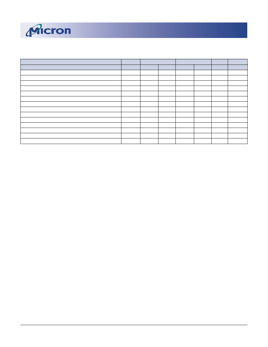
READ CYCLE
NOTE: 1.
t
OFF is referenced from rising edge of RAS# or CAS#, whichever occurs last.
tRRH
tCLZ
tCAC
tRAC
tAA
VALID DATA
OPEN
tOFF
tRCH
ROW
tRCS
tASC
tACH
tRAH
tRAD
tAR
tCAH
tRCD
tCAS
tRSH
tCSH
tRP
tRC
tRAS
tCRP
tASR
ROW
OPEN
RAS#
V
V
IH
IL
V
V
IH
IL
ADDR
V
V
IH
IL
DQ
V
V
OH
OL
V
V
IH
IL
COLUMN
CAS#
WE#
NOTE 1
DON'T CARE
UNDEFINED
TIMING PARAMETERS
-5
-6
SYMBOL
MIN
MAX
MIN
MAX
UNITS
t
AA
25
30
ns
t
AR
38
45
ns
t
ASC
0
0
ns
t
ASR
0
0
ns
t
CAC
13
15
ns
t
CAH
8
10
ns
t
CAS
8
10,000
10
10,000
ns
t
CLZ
0
0
ns
t
CRP
5
5
ns
t
CSH
38
45
ns
t
OFF
0
12
0
15
ns
-5
-6
SYMBOL
MIN
MAX
MIN
MAX
UNITS
t
RAC
50
60
ns
t
RAD
9
12
ns
t
RAH
9
10
ns
t
RAS
50
10,000
60
10,000
ns
t
RC
84
104
ns
t
RCD
11
14
ns
t
RCH
0
0
ns
t
RCS
0
0
ns
t
RP
30
40
ns
t
RRH
0
0
ns
t
RSH
13
15
ns

4, 8 Meg x 36 ECC-Optimized DRAM SIMMs
Micron Technology, Inc., reserves the right to change products or specifications without notice.
DM65_2.p65 ≠ Rev. 9/98
©1998, Micron Technology, Inc.
10
4, 8 MEG x 36
ECC-OPTIMIZED DRAM SIMMs
NOT RECOMMENDED FOR NEW DESIGNS
DON'T CARE
UNDEFINED
V
V
IH
IL
VALID DATA
ROW
COLUMN
ROW
tDS
tWP
tWCH
tWCS
tWCR
tRWL
tCWL
tCAH
tASC
tRAH
tASR
tRAD
tAR
tCAS
tRSH
tCSH
tRCD
tCRP
tRAS
tRC
tRP
V
V
IH
IL
ADDR
V
V
IH
IL
V
V
IH
IL
DQ
V
V
IOH
IOL
RAS#
tDH
WE#
CAS#
tACH
EARLY WRITE CYCLE
-5
-6
SYMBOL
MIN
MAX
MIN
MAX
UNITS
t
RAH
9
10
ns
t
RAS
50
10,000
60
10,000
ns
t
RC
84
104
ns
t
RCD
11
14
ns
t
RP
30
40
ns
t
RSH
13
15
ns
t
RWL
13
15
ns
t
WCH
8
10
ns
t
WCR
38
45
ns
t
WCS
0
0
ns
t
WP
5
5
ns
TIMING PARAMETERS
-5
-6
SYMBOL
MIN
MAX
MIN
MAX
UNITS
t
ACH
12
15
ns
t
AR
38
45
ns
t
ASC
0
0
ns
t
ASR
0
0
ns
t
CAH
8
10
ns
t
CAS
8
10,000
10
10,000
ns
t
CRP
5
5
ns
t
CSH
38
45
ns
t
CWL
8
10
ns
t
DH
8
10
ns
t
DS
0
0
ns
t
RAD
9
12
ns
4, 8 Meg x 36 ECC-Optimized DRAM SIMMs
Micron Technology, Inc., reserves the right to change products or specifications without notice.
DM65_2.p65 ≠ Rev. 9/98
©1998, Micron Technology, Inc.
11
4, 8 MEG x 36
ECC-OPTIMIZED DRAM SIMMs
NOT RECOMMENDED FOR NEW DESIGNS
VALID
DATA
VALID
DATA
VALID
DATA
COLUMN
COLUMN
COLUMN
ROW
ROW
DON'T CARE
UNDEFINED
tCAH
tASC
tCP
tRSH
tCP
tCP
tCAS
tRCD
tCRP
tPC
tCSH
tRASP
tRP
tCAH
tASC
tCAH
tASC
tAR
tRAH
tRAD
tACH
tACH
tACH
tASR
tRCS
tRRH
tRCH
tOFF
tCAC
tCPA
tAA
tCLZ
tCAC
tCPA
tAA
tCAC
tRAC
tAA
tCLZ
OPEN
OPEN
V
V
IH
IL
V
V
IH
IL
ADDR
V
V
IH
IL
V
V
IH
IL
DQ
V
V
OH
OL
RAS#
tCAS
tCAS
CAS#
WE#
tCOH
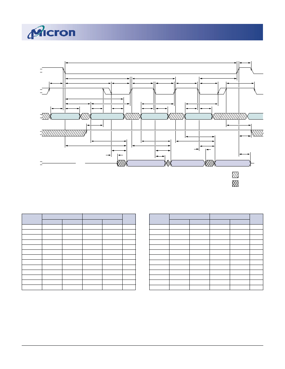
EDO-PAGE-MODE READ CYCLE
-5
-6
SYMBOL
MIN
MAX
MIN
MAX
UNITS
t
CSH
38
45
ns
t
OFF
0
12
0
15
ns
t
PC
20
25
ns
t
RAC
50
60
ns
t
RAD
9
12
ns
t
RAH
9
10
ns
t
RASP
50
125,000
60
125,000
ns
t
RCD
11
14
ns
t
RCH
0
0
ns
t
RCS
0
0
ns
t
RP
30
40
ns
t
RRH
0
0
ns
t
RSH
13
15
ns
TIMING PARAMETERS
-5
-6
SYMBOL
MIN
MAX
MIN
MAX
UNITS
t
AA
25
30
ns
t
ACH
12
15
ns
t
AR
38
45
ns
t
ASC
0
0
ns
t
ASR
0
0
ns
t
CAC
13
15
ns
t
CAH
8
10
ns
t
CAS
8
10,000
10
10,000
ns
t
CLZ
0
0
ns
t
COH
3
3
ns
t
CP
8
10
ns
t
CPA
28
35
ns
t
CRP
5
5
ns
4, 8 Meg x 36 ECC-Optimized DRAM SIMMs
Micron Technology, Inc., reserves the right to change products or specifications without notice.
DM65_2.p65 ≠ Rev. 9/98
©1998, Micron Technology, Inc.
12
4, 8 MEG x 36
ECC-OPTIMIZED DRAM SIMMs
NOT RECOMMENDED FOR NEW DESIGNS
tDS
tDH
tDS
tDH
tDS
tDH
tWCR
VALID DATA
VALID DATA
VALID DATA
tRWL
tWP
tCWL
tWCH
tWCS
tWP
tCWL
tWCH
tWCS
tWP
tCWL
tWCH
tWCS
tCAH
tASC
tCAH
tASC
tCAH
tASC
tRAH
tASR
tRAD
tAR
COLUMN
COLUMN
COLUMN
ROW
ROW
tCP
tCAS
tRSH
tCP
tCAS
tCP
tCAS
tRCD
tCRP
tPC
tCSH
tRASP
tRP
V
V
IH
IL
CAS#
V
V
IH
IL
ADDR
V
V
IH
IL
WE#
V
V
IH
IL
DQ
V
V
IOH
IOL
RAS#
DON'T CARE
UNDEFINED
tACH
tACH
tACH
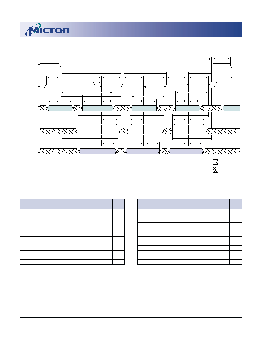
EDO-PAGE-MODE EARLY-WRITE CYCLE
t
PC
20
25
ns
t
RAD
9
12
ns
t
RAH
9
10
ns
t
RASP
50
125,000
60
125,000
ns
t
RCD
11
14
ns
t
RP
30
40
ns
t
RSH
13
15
ns
t
RWL
13
15
ns
t
WCH
8
10
ns
t
WCR
38
45
ns
t
WCS
0
0
ns
t
WP
5
5
ns
-5
-6
SYMBOL
MIN
MAX
MIN
MAX
UNITS
TIMING PARAMETERS
-5
-6
SYMBOL
MIN
MAX
MIN
MAX
UNITS
t
ACH
12
15
ns
t
AR
38
45
ns
t
ASC
0
0
ns
t
ASR
0
0
ns
t
CAH
8
10
ns
t
CAS
8
10,000
10
10,000
ns
t
CP
8
10
ns
t
CRP
5
5
ns
t
CSH
38
45
ns
t
CWL
8
10
ns
t
DH
8
10
ns
t
DS
0
0
ns
4, 8 Meg x 36 ECC-Optimized DRAM SIMMs
Micron Technology, Inc., reserves the right to change products or specifications without notice.
DM65_2.p65 ≠ Rev. 9/98
©1998, Micron Technology, Inc.
13
4, 8 MEG x 36
ECC-OPTIMIZED DRAM SIMMs
NOT RECOMMENDED FOR NEW DESIGNS
V
V
IH
IL
V
V
IH
IL
RAS#
V
V
IH
IL
ADDR
V
V
IH
IL
WE#
tRASP
tRP
ROW
COLUMN (A)
COLUMN (N)
ROW
V
V
IOH
IOL
tCRP
tCSH
tCAS
tRCD
tASR
tRAH
tRAD
tASC
tAR
tCAH
tASC
tCAH
tASC
tCAH
tCP
tRSH
VALID DATA
IN
tRCS
tRCH
tWCS
VALID
DATA (B)
VALID DATA (A)
tWHZ
tCAC
tCPA
tAA
tCAC
tAA
OPEN
DQ
tPC
RAC
t
tCOH
tWCH
tDS
tDH
tPC
COLUMN (B)
tACH
CAS#
tCAS
tCAS
tCP
tCP
DON'T CARE
UNDEFINED
EDO-PAGE-MODE READ-EARLY-WRITE CYCLE
(Pseudo READ-MODIFY-WRITE)
t
DS
0
0
ns
t
PC
20
25
ns
t
RAC
50
60
ns
t
RAD
9
12
ns
t
RAH
9
10
ns
t
RASP
50
125,000
60
125,000
ns
t
RCD
11
14
ns
t
RCH
0
0
ns
t
RCS
0
0
ns
t
RP
30
40
ns
t
RSH
13
15
ns
t
WCH
8
10
ns
t
WCS
0
0
ns
t
WHZ
0
12
0
15
ns
-5
-6
SYMBOL
MIN
MAX
MIN
MAX
UNITS
TIMING PARAMETERS
-5
-6
SYMBOL
MIN
MAX
MIN
MAX
UNITS
t
AA
25
30
ns
t
ACH
12
15
ns
t
AR
38
45
ns
t
ASC
0
0
ns
t
ASR
0
0
ns
t
CAC
13
15
ns
t
CAH
8
10
ns
t
CAS
8
10,000
10
10,000
ns
t
COH
3
3
ns
t
CP
8
10
ns
t
CPA
28
35
ns
t
CRP
5
5
ns
t
CSH
38
45
ns
t
DH
8
10
ns
4, 8 Meg x 36 ECC-Optimized DRAM SIMMs
Micron Technology, Inc., reserves the right to change products or specifications without notice.
DM65_2.p65 ≠ Rev. 9/98
©1998, Micron Technology, Inc.
14
4, 8 MEG x 36
ECC-OPTIMIZED DRAM SIMMs
NOT RECOMMENDED FOR NEW DESIGNS
tCLZ
tCAC
tRAC
tAA
VALID DATA
OPEN
tRCH
tRCS
tASC
tRAH
tRAD
tAR
tCAH
tRCD
tCAS
tCSH
tCRP
tASR
ROW
OPEN
RAS#
V
V
IH
IL
V
V
IH
IL
ADDR
V
V
IH
IL
DQ
V
V
OH
OL
V
V
IH
IL
COLUMN
CAS#
WE#
tWHZ
tWPZ
tCP
tASC
tRCS
COLUMN
tCLZ
DON'T CARE
UNDEFINED
EDO READ CYCLE
(with WE#-controlled disable)
-5
-6
SYMBOL
MIN
MAX
MIN
MAX
UNITS
t
CSH
38
45
ns
t
RAC
50
60
ns
t
RAD
9
12
ns
t
RAH
9
10
ns
t
RCD
11
14
ns
t
RCH
0
0
ns
t
RCS
0
0
ns
t
WHZ
0
12
0
15
ns
t
WPZ
10
10
ns
TIMING PARAMETERS
-5
-6
SYMBOL
MIN
MAX
MIN
MAX
UNITS
t
AA
25
30
ns
t
AR
38
45
ns
t
ASC
0
0
ns
t
ASR
0
0
ns
t
CAC
13
15
ns
t
CAH
8
10
ns
t
CAS
8
10,000
10
10,000
ns
t
CLZ
0
0
ns
t
CP
8
10
ns
t
CRP
5
5
ns
4, 8 Meg x 36 ECC-Optimized DRAM SIMMs
Micron Technology, Inc., reserves the right to change products or specifications without notice.
DM65_2.p65 ≠ Rev. 9/98
©1998, Micron Technology, Inc.
15
4, 8 MEG x 36
ECC-OPTIMIZED DRAM SIMMs
NOT RECOMMENDED FOR NEW DESIGNS
RAS#-ONLY REFRESH CYCLE
ROW
V
V
IH
IL
CAS#
V
V
IH
IL
ADDR
V
V
IH
IL
RAS#
tRC
tRAS
tRP
tCRP
tASR
tRAH
ROW
OPEN
DQ
V
V
OH
OL
tRPC
WE#
V
V
IH
IL
CBR REFRESH CYCLE
(Addresses = DON'T CARE)
tRP
V
V
IH
IL
RAS#
tRAS
OPEN
tCHR
tCSR
V
V
IH
IL
V
V
OH
OL
CAS#
DQ
tRP
tRAS
tRPC
tCSR
tRPC
tCHR
tCP
V
V
IH
IL
tWRP
tWRH
tWRP
tWRH
WE#
DON'T CARE
UNDEFINED
NOTE 1
-5
-6
SYMBOL
MIN
MAX
MIN
MAX
UNITS
t
RAS
50
10,000
60
10,000
ns
t
RC
84
104
ns
t
RP
30
40
ns
t
RPC
5
5
ns
t
WRH
8
10
ns
t
WRP
8
10
ns
TIMING PARAMETERS
-5
-6
SYMBOL
MIN
MAX
MIN
MAX
UNITS
t
ASR
0
0
ns
t
CHR
8
10
ns
t
CP
8
10
ns
t
CRP
5
5
ns
t
CSR
5
5
ns
t
RAH
9
10
ns

4, 8 Meg x 36 ECC-Optimized DRAM SIMMs
Micron Technology, Inc., reserves the right to change products or specifications without notice.
DM65_2.p65 ≠ Rev. 9/98
©1998, Micron Technology, Inc.
16
4, 8 MEG x 36
ECC-OPTIMIZED DRAM SIMMs
NOT RECOMMENDED FOR NEW DESIGNS
DON'T CARE
UNDEFINED
tCLZ
tOFF
OPEN
VALID DATA
OPEN
COLUMN
ROW
tCAC
tRAC
tAA
tCAH
tASC
tRAH
tASR
tRAD
tAR
tCRP
tRCD
tRSH
tRAS
tRP
tCHR
tRAS
DQ
V
V
OH
OL
V
V
IH
IL
ADDR
V
V
IH
IL
V
V
IH
IL
RAS#
CAS#
HIDDEN REFRESH CYCLE
20
(WE# = HIGH)
-5
-6
SYMBOL
MIN
MAX
MIN
MAX
UNITS
t
OFF
0
12
0
15
ns
t
RAC
50
60
ns
t
RAD
9
12
ns
t
RAH
9
10
ns
t
RAS
50
10,000
60
10,000
ns
t
RCD
11
14
ns
t
RP
30
40
ns
t
RSH
13
15
ns
TIMING PARAMETERS
-5
-6
SYMBOL
MIN
MAX
MIN
MAX
UNITS
t
AA
25
30
ns
t
AR
38
45
ns
t
ASC
0
0
ns
t
ASR
0
0
ns
t
CAC
13
15
ns
t
CAH
8
10
ns
t
CHR
8
10
ns
t
CLZ
0
0
ns
t
CRP
5
5
ns
4, 8 Meg x 36 ECC-Optimized DRAM SIMMs
Micron Technology, Inc., reserves the right to change products or specifications without notice.
DM65_2.p65 ≠ Rev. 9/98
©1998, Micron Technology, Inc.
17
4, 8 MEG x 36
ECC-OPTIMIZED DRAM SIMMs
NOT RECOMMENDED FOR NEW DESIGNS
72-Pin SIMM
(16MB)
72-Pin SIMM
(32MB)
.050 (1.27)
TYP
1.010 (25.65)
.990 (25.15)
PIN 1
.200 (5.08)
MAX
.054 (1.37)
.047 (1.19)
4.260 (108.20)
4.240 (107.70)
.133 (3.38)
TYP
.400 (10.16)
TYP
.080 (2.03)
.040 (1.02)
TYP
.125 (3.18)
TYP
.235 (5.97)
MIN
.250 (6.35)
.250 (6.35)
1.75 (44.45) TYP
3.75 (95.25)
.050 (1.27)
TYP
1.010 (25.65)
.990 (25.15)
PIN 1
.350 (8.98)
MAX
.054 (1.37)
.047 (1.19)
4.260 (108.20)
4.240 (107.70)
.133 (3.38)
TYP
.400 (10.16)
TYP
.080 (2.03)
.040 (1.02)
TYP
.125 (3.18)
TYP
.235 (5.97)
MIN
.250 (6.35)
.250 (6.35)
1.75 (44.45) TYP
3.75 (95.25)
8000 S. Federal Way, P.O. Box 6, Boise, ID 83707-0006, Tel: 208-368-3900
E-mail: prodmktg@micron.com, Internet: http://www.micron.com, Customer Comment Line: 800-932-4992
Micron is a registered trademark and the Micron logo and M logo are trademarks of Micron Technology, Inc.