
2, 4 Meg x 72 Nonbuffered DRAM DIMMs
Micron Technology, Inc., reserves the right to change products or specifications without notice.
DM60.p65 ≠ Rev. 6/98
©
1998, Micron Technology, Inc.
1
2, 4 MEG x 72
NONBUFFERED DRAM DIMMs
OBSOLETE
DRAM
MODULE
MT9LD272A(X), MT18LD472A(X)
For the latest data sheet revisions, please refer to the Micron
Web site: www.micron.com/mti/msp/html/datasheet.html
FEATURES
∑ JEDEC-standard, eight-CAS#, ECC pinout in a 168-pin,
dual in-line memory module (DIMM)
∑ 16MB (2 Meg x 72) and 32MB (4 Meg x 72)
∑ Nonbuffered
∑ High-performance CMOS silicon-gate process
∑ Single +3.3V
±
0.3V power supply
∑ All inputs, outputs and clocks are TTL-compatible
∑ Refresh modes: RAS#-ONLY, CAS#-BEFORE-RAS#
(CBR) and HIDDEN
∑ 2,048-cycle refresh distributed across 32ms
∑ FAST-PAGE-MODE (FPM) or Extended Data-Out
(EDO) PAGE MODE access cycles
∑ Serial presence-detect (SPD)
OPTIONS
MARKING
∑ Package
168-pin DIMM (gold)
G
∑ Timing
50ns access
-5*
60ns access
-6
∑ Access Cycles
FAST PAGE MODE
None
EDO PAGE MODE
X
*EDO version only
PIN
SYMBOL
PIN
SYMBOL
PIN
SYMBOL
PIN
SYMBOL
1
V
SS
43
V
SS
85
V
SS
127
V
SS
2
DQ0
44
OE2#
86
DQ32
128
RFU
3
DQ1
45
RAS2#
87
DQ33
129 NC/RAS3#*
4
DQ2
46
CAS2#
88
DQ34
130
CAS6#
5
DQ3
47
CAS3#
89
DQ35
131
CAS7#
6
V
DD
48
WE2#
90
V
DD
132
RFU
7
DQ4
49
V
DD
91
DQ36
133
V
DD
8
DQ5
50
NC
92
DQ37
134
NC
9
DQ6
51
NC
93
DQ38
135
NC
10
DQ7
52
CB2
94
DQ39
136
CB6
11
DQ8
53
CB3
95
DQ40
137
CB7
12
V
SS
54
V
SS
96
V
SS
138
V
SS
13
DQ9
55
DQ16
97
DQ41
139
DQ48
14
DQ10
56
DQ17
98
DQ42
140
DQ49
15
DQ11
57
DQ18
99
DQ43
141
DQ50
16
DQ12
58
DQ19
100
DQ44
142
DQ51
17
DQ13
59
V
DD
101
DQ45
143
V
DD
18
V
DD
60
DQ20
102
V
DD
144
DQ52
19
DQ14
61
NC
103
DQ46
145
NC
20
DQ15
62
RFU
104
DQ47
146
RFU
21
CB0
63
NC
105
CB4
147
NC
22
CB1
64
V
SS
106
CB5
148
V
SS
23
V
SS
65
DQ21
107
V
SS
149
DQ53
24
NC
66
DQ22
108
NC
150
DQ54
25
NC
67
DQ23
109
NC
151
DQ55
26
V
DD
68
V
SS
110
V
DD
152
V
SS
27
WE0#
69
DQ24
111
RFU
153
DQ56
28
CAS0#
70
DQ25
112
CAS4#
154
DQ57
29
CAS1#
71
DQ26
113
CAS5#
155
DQ58
30
RAS0#
72
DQ27
114
NC
156
DQ59
31
OE0#
73
V
DD
115
RFU
157
V
DD
32
V
SS
74
DQ28
116
V
SS
158
DQ60
33
A0
75
DQ29
117
A1
159
DQ61
34
A2
76
DQ30
118
A3
160
DQ62
35
A4
77
DQ31
119
A5
161
DQ63
36
A6
78
V
SS
120
A7
162
V
SS
37
A8
79
NC
121
A9
163
NC
38
A10
80
NC
122
NC (A11)
164
NC
39
NC (A12)
81
NC
123
NC (A13)
165
SA0
40
V
DD
82
SDA
124
V
DD
166
SA1
41
V
DD
83
SCL
125
RFU
167
SA2
42
RFU
84
V
DD
126
RFU
168
V
DD
PIN ASSIGNMENT (Front View)
168-Pin DIMM
KEY TIMING PARAMETERS
EDO Operating Mode
SPEED
t
RC
t
RAC
t
PC
t
AA
t
CAC
t
CAS
-5
84ns
50ns
20ns
25ns
13ns
8ns
-6
104ns
60ns
25ns
30ns
15ns
10ns
FPM Operating Mode
SPEED
t
RC
t
RAC
t
PC
t
AA
t
CAC
t
RP
-6
110ns
60ns
35ns
30ns
15ns
40ns
NOTE: Pin symbols in parentheses are not used on these modules but may be used
for other modules in this product family. They are for reference only.

2, 4 Meg x 72 Nonbuffered DRAM DIMMs
Micron Technology, Inc., reserves the right to change products or specifications without notice.
DM60.p65 ≠ Rev. 6/98
©
1998, Micron Technology, Inc.
2
2, 4 MEG x 72
NONBUFFERED DRAM DIMMs
OBSOLETE
PART NUMBERS
EDO Operating Mode
PART NUMBER
CONFIGURATION
SPEED
MT9LD272AG-5 X
2 Meg x 72 ECC
50ns
MT9LD272AG-6 X
2 Meg x 72 ECC
60ns
MT18LD472AG-5 X
4 Meg x 72 ECC
50ns
MT18LD472AG-6 X
4 Meg x 72 ECC
60ns
FPM Operating Mode
PART NUMBER
CONFIGURATION
SPEED
MT9LD272AG-6
2 Meg x 72 ECC
60ns
MT18LD472AG-6
4 Meg x 72 ECC
60ns
EDO PAGE MODE
EDO PAGE MODE, designated by the "X" version, is an
accelerated FAST-PAGE-MODE cycle. The primary advan-
tage of EDO is the availability of data-out even after CAS#
goes back HIGH. EDO provides for CAS# precharge time
(
t
CP) to occur without the output data going invalid. This
elimination of CAS# output control provides for pipelined
READs.
FAST-PAGE-MODE modules have traditionally turned
the output buffers off (High-Z) with the rising edge of
CAS#. EDO-PAGE-MODE DRAMs operate like FAST-
PAGE-MODE DRAMs, except data will remain valid or
become valid after CAS# goes HIGH during READs, pro-
vided RAS# and OE# are held LOW. If OE# is pulsed while
RAS# and CAS# are LOW, data will toggle from valid data
to High-Z and back to the same valid data. If OE# is toggled
or pulsed after CAS# goes HIGH while RAS# remains
LOW, data will transition to and remain High-Z.
During an application, if the DQ outputs are wire OR'd,
OE# must be used to disable idle banks of DRAMs. Alterna-
tively, pulsing WE# to the idle banks during CAS# HIGH
time will also High-Z the outputs. Independent of OE#
control, the outputs will disable after
t
OFF, which is refer-
enced from the rising edge of RAS# or CAS#, whichever
occurs last. (Refer to the 4 Meg x 4 [MT4LC4M4E8] DRAM
data sheet for additional information on EDO functional-
ity.)
REFRESH
Returning RAS# and CAS# HIGH terminates a memory
cycle and decreases chip current to a reduced standby level.
Also, the chip is preconditioned for the next cycle during
the RAS# HIGH time. Correct memory cell data is pre-
served by maintaining power and executing any RAS#
cycle (READ, WRITE) or RAS# REFRESH cycle (RAS#-
ONLY, CBR or HIDDEN) so that all combinations of RAS#
addresses (A0-A9/A10) are executed at least every
t
REF,
regardless of sequence. The CBR REFRESH cycle will in-
voke the internal refresh counter for automatic RAS# ad-
dressing.
SERIAL PRESENCE-DETECT OPERATION
This module family incorporates serial presence-detect
(SPD). The SPD function is implemented using a 2,048-bit
EEPROM. This nonvolatile storage device contains 256
bytes. The first 128 bytes can be programmed by Micron to
identify the module type and various DRAM organizations
and timing parameters. The remaining 128 bytes of storage
are available for use by the customer. System READ/
WRITE operations between the master (system logic) and
the slave EEPROM device (DIMM) occur via a standard IIC
bus using the DIMM's SCL (clock) and SDA (data) signals,
GENERAL DESCRIPTION
The MT9LD272A(X) and MT18LD472A(X) are randomly
accessed 16MB and 32MB memories organized in a x72
configuration. They are specially processed to operate from
3V to 3.6V for low-voltage memory systems.
During READ or WRITE cycles, each bit is uniquely
addressed through the 21/22 address bits, which are en-
tered 11 bits (A0 -A10) at RAS# time and 10/11 bits (A0-
A10) at CAS# time.
READ and WRITE cycles are selected with the WE#
input. A logic HIGH on WE# dictates read mode, while a
logic LOW on WE# dictates write mode. During a WRITE
cycle, data-in (D) is latched by the falling edge of WE# or
CAS#, whichever occurs last. An EARLY WRITE occurs
when WE# is taken LOW prior to CAS# falling. A LATE
WRITE or READ-MODIFY-WRITE occurs when WE# falls
after CAS# was taken LOW. During EARLY WRITE cycles,
the data-outputs (Q) will remain High-Z regardless of the
state of OE#. During LATE WRITE or READ-MODIFY-
WRITE cycles, OE# must be taken HIGH to disable the data-
outputs prior to applying input data. If a LATE WRITE or
READ-MODIFY-WRITE is attempted while keeping OE#
LOW, no WRITE will occur, and the data-outputs will drive
read data from the accessed location.
FAST PAGE MODE
FAST-PAGE-MODE operations allow faster data opera-
tions (READ or WRITE) within a row-address-defined
page boundary. The FAST-PAGE-MODE cycle is always
initiated with a row address strobed in by RAS#, followed
by a column address strobed in by CAS#. Additional col-
umns may be accessed by providing valid column
addresses, strobing CAS# and holding RAS# LOW , thus
executing faster memory cycles. Returning RAS# HIGH
terminates the FAST-PAGE-MODE operation.
2, 4 Meg x 72 Nonbuffered DRAM DIMMs
Micron Technology, Inc., reserves the right to change products or specifications without notice.
DM60.p65 ≠ Rev. 6/98
©
1998, Micron Technology, Inc.
3
2, 4 MEG x 72
NONBUFFERED DRAM DIMMs
OBSOLETE
together with SA(2:0), which provide eight unique DIMM/
EEPROM addresses.
SPD CLOCK AND DATA CONVENTIONS
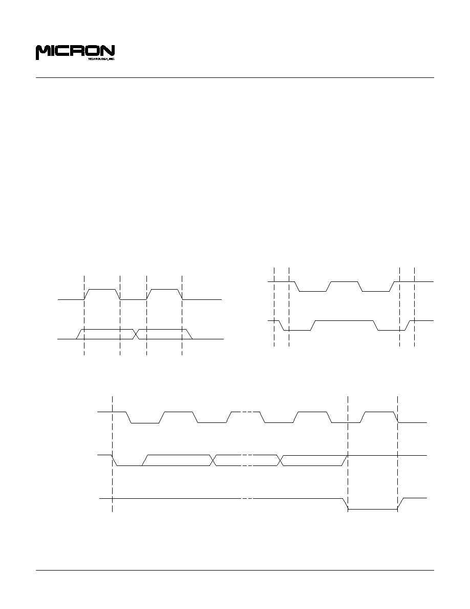
Data states on the SDA line can change only during SCL
LOW. SDA state changes during SCL HIGH are reserved
for indicating start and stop conditions (Figures 1 and 2).
SPD START CONDITION
All commands are preceded by the start condition, which
is a HIGH-to-LOW transition of SDA when SCL is HIGH.
The SPD device continuously monitors the SDA and SCL
lines for the start condition and will not respond to any
command until this condition has been met.
SPD STOP CONDITION
All communications are terminated by a stop condition,
which is a LOW-to-HIGH transition of SDA when SCL is
HIGH. The stop condition is also used to place the SPD
device into standby power mode.
SPD ACKNOWLEDGE
Acknowledge is a software convention used to indicate
successful data transfers. The transmitting device, either
master or slave, will release the bus after transmitting eight
bits. During the ninth clock cycle, the receiver will pull the
SDA line LOW to acknowledge that it received the eight bits
of data (Figure 3).
The SPD device will always respond with an acknowl-
edge after recognition of a start condition and its slave
address. If both the device and a write operation have been
selected, the SPD device will respond with an acknowledge
after the receipt of each subsequent eight-bit word. In the
read mode the SPD device will transmit eight bits of data,
release the SDA line and monitor the line for an acknowl-
edge. If an acknowledge is detected and no stop condition
is generated by the master, the slave will continue to trans-
mit data. If an acknowledge is not detected, the slave will
terminate further data transmissions and await the stop
condition to return to standby power mode.
SCL
SDA
DATA STABLE
DATA STABLE
DATA
CHANGE
Figure 1
DATA VALIDITY
SCL
SDA
START
BIT
STOP
BIT
Figure 2
DEFINITION OF START AND STOP
SCL from Master
Data Output
from Transmitter
Data Output
from Receiver
9
8
Acknowledge
Figure 3
ACKNOWLEDGE RESPONSE FROM RECEIVER

2, 4 Meg x 72 Nonbuffered DRAM DIMMs
Micron Technology, Inc., reserves the right to change products or specifications without notice.
DM60.p65 ≠ Rev. 6/98
©
1998, Micron Technology, Inc.
4
2, 4 MEG x 72
NONBUFFERED DRAM DIMMs
OBSOLETE
FUNCTIONAL BLOCK DIAGRAM
MT9LD272A(X) (16MB)
A0-A10
OE2#
WE2#
CAS4#
RAS2#
CAS5#
CAS7#
CAS6#
U1-U9 = MT4LC2M8B1 FAST PAGE MODE
U1-U9 = MT4LC2M8E7 EDO PAGE MODE
OE0#
WE0#
CAS0#
RAS0#
CAS1#
CAS3#
CAS2#
11
11
11
11
11
11
11
11
11
DQ0-DQ7
DQ8-DQ15
CB0-CB7
DQ16-DQ23
DQ32-DQ39
DQ40-DQ41
DQ48-DQ55
DQ56-DQ63
DQ24-DQ31
U1
A0≠A10
WE#
OE#
RAS#
CAS#
DQ0-DQ7
U2
A0≠A10
WE#
OE#
RAS#
CAS#
DQ0-DQ7
U3
A0≠A10
WE#
OE#
RAS#
CAS#
DQ0-DQ7
U4
A0≠A10
WE#
OE#
RAS#
CAS#
DQ0-DQ7
U6
A0≠A10
WE#
OE#
RAS#
CAS#
DQ0-DQ7
U7
A0≠A10
WE#
OE#
RAS#
CAS#
DQ0-DQ7
U8
A0≠A10
WE#
OE#
RAS#
CAS#
DQ0-DQ7
U9
A0≠A10
WE#
OE#
RAS#
CAS#
DQ0-DQ7
U5
A0≠A10
WE#
OE#
RAS#
CAS#
SPD
SCL
SDA
SA0 SA1 SA2
A0
A1
A2
V
DD
V
SS
U1-U9
U1-U9

2, 4 Meg x 72 Nonbuffered DRAM DIMMs
Micron Technology, Inc., reserves the right to change products or specifications without notice.
DM60.p65 ≠ Rev. 6/98
©
1998, Micron Technology, Inc.
5
2, 4 MEG x 72
NONBUFFERED DRAM DIMMs
OBSOLETE
FUNCTIONAL BLOCK DIAGRAM
MT18LD472A(X) (32MB)
U1-U18 = MT4LC4M4B1 FAST PAGE MODE
U1-U18 = MT4LC4M4E8 EDO PAGE MODE
11
11
11
11
11
11
11
11
11
11
11
11
11
11
11
11
OE0#
CAS1#
CAS2#
CAS3#
WE0#
CAS0#
OE2#
CAS5#
CAS6#
CAS7#
WE2#
CAS4#
A0-A10
RAS0#
RAS2#
11
11
SPD
SCL
SDA
A0
A1
A2
SA0
SA1
SA2
WE#
OE#
RAS#
CAS#
DQ0-DQ3
U1
A0≠A10
WE#
OE#
RAS#
CAS#
DQ0-DQ3
U2
A0≠A10
WE#
OE#
RAS#
CAS#
DQ0-DQ3
U3
A0≠A10
WE#
OE#
RAS#
CAS#
DQ0-DQ3
U4
A0≠A10
WE#
OE#
RAS#
CAS#
DQ0-DQ3
U5
A0≠A10
WE#
OE#
RAS#
CAS#
DQ0-DQ3
U6
A0≠A10
WE#
OE#
RAS#
CAS#
DQ0-DQ3
U7
A0≠A10
WE#
OE#
RAS#
CAS#
DQ0-DQ3
U8
A0≠A10
WE#
OE#
RAS#
CAS#
DQ0-DQ3
U9
A0≠A10
WE#
OE#
RAS#
CAS#
DQ0-DQ3
U10
A0≠A10
WE#
OE#
RAS#
CAS#
DQ0-DQ3
U11
A0≠A10
WE#
OE#
RAS#
CAS#
DQ0-DQ3
U12
A0≠A10
WE#
OE#
RAS#
CAS#
DQ0-DQ3
U13
A0≠A10
WE#
OE#
RAS#
CAS#
DQ0-DQ3
U14
A0≠A10
WE#
OE#
RAS#
CAS#
DQ0-DQ3
U15
A0≠A10
WE#
OE#
RAS#
CAS#
DQ0-DQ3
U16
A0≠A10
WE#
OE#
RAS#
CAS#
DQ0-DQ3
U17
A0≠A10
WE#
OE#
RAS#
CAS#
DQ0-DQ3
DQ0-DQ3
DQ4-DQ7
DQ8-DQ11
DQ12-DQ15
DQ16-DQ19
DQ20-DQ23
DQ24-DQ27
DQ28-DQ31
DQ32-DQ35
DQ36-DQ39
DQ40-DQ43
DQ44-DQ47
CB4-CB7
CB4-CB7
DQ48-DQ51
DQ52-DQ55
DQ56-DQ59
DQ06-DQ63
U18
A0≠A10
V
DD
V
SS
U1-U18
U1-U18

2, 4 Meg x 72 Nonbuffered DRAM DIMMs
Micron Technology, Inc., reserves the right to change products or specifications without notice.
DM60.p65 ≠ Rev. 6/98
©
1998, Micron Technology, Inc.
6
2, 4 MEG x 72
NONBUFFERED DRAM DIMMs
OBSOLETE
PIN DESCRIPTIONS
PIN NUMBERS
SYMBOL
TYPE
DESCRIPTION
30, 45
RAS0#, RAS2#
Input
Row-Address Strobe: RAS# is used to clock-in the row-
address bits. Two RAS# inputs allow for one x72 bank or
two x36 banks.
28, 29, 46, 47, 112,
CAS0#-CAS7#
Input
Column-Address Strobe: CAS# is used to clock-in the
113, 130, 131
column-address bits, enable the DRAM output buffers
and strobe the data inputs on WRITE cycles. Eight CAS#
inputs allow byte access control for any memory bank
configuration.
27, 48
WE0#, WE2#
Input
Write Enable: WE# is the READ/WRITE control for the
DQ pins. If WE# is LOW prior to CAS# going LOW, the
access is an EARLY WRITE cycle. If WE# is HIGH while
CAS# is LOW, the access is a READ cycle, provided OE#
is also LOW. If WE# goes LOW after CAS# goes LOW,
then the cycle is a LATE WRITE cycle. A LATE WRITE
cycle is generally used in conjunction with a READ cycle
to form a READ-MODIFY-WRITE cycle.
31, 44
OE0#, OE2#
Input
Output Enable: OE# is the input/output control for the DQ
pins. These signals may be driven, allowing LATE WRITE
cycles.
33-38, 117-121
A0-A10
Input
Address Inputs: These inputs are multiplexed and clocked
by RAS# and CAS#.
2-5, 7-11, 13-17, 19-20,
DQ0-DQ63
Input/
Data I/O: For WRITE cycles, DQ0-DQ63 act as inputs to
55-58, 60, 65-67, 69-72,
Output
the addressed DRAM location. For READ access cycles,
74-77, 86-89,91-95,
DQ0-DQ63 act as outputs for the addressed DRAM
97-101, 103-104,
location.
139-142, 144, 149-151,
153-156, 158-161
21-22, 52-53, 105-106,
CB0-CB7
Input/Output
Check Bits.
136-137
42, 62, 111, 115,
RFU
≠
Reserved for Future Use: These pins should be left
125-126, 128, 132, 146
unconnected.
6, 18, 26, 40, 41, 49, 59,
V
DD
Supply
Power Supply: +3.3V
±
0.3V.
73, 84, 90, 102, 110,
124, 133, 143, 157, 168
1, 12, 23, 32, 43, 54, 64,
V
SS
Supply
Ground.
68, 78, 85, 96, 107, 116,
127, 138, 148, 152, 162
82
SDA
Input/Output
Serial Presence-Detect Data. SDA is a bidirectional pin
used to transfer addresses and data into and data out of
the presence-detect portion of the module.
83
SCL
Input
Serial Clock for Presence-Detect. SCL is used to
synchronize the presence-detect data transfer to and
from the module.
165-167
SA0-SA2
Input
Presence-Detect Address Inputs. These pins are used to
configure the presence-detect device.

2, 4 Meg x 72 Nonbuffered DRAM DIMMs
Micron Technology, Inc., reserves the right to change products or specifications without notice.
DM60.p65 ≠ Rev. 6/98
©
1998, Micron Technology, Inc.
7
2, 4 MEG x 72
NONBUFFERED DRAM DIMMs
OBSOLETE
SERIAL PRESENCE-DETECT MATRIX
BYTE
DESCRIPTION
ENTRY (VERSION)
BIT7
BIT6
BIT5
BIT4
BIT3
BIT2
BIT1
BIT0
HEX
0
NUMBER OF BYTES USED BY MICRON
128
1
0
0
0
0
0
0
0
80
1
TOTAL NUMBER OF SPD MEMORY BYTES
256
0
0
0
0
1
0
0
0
08
2
MEMORY TYPE
FAST PAGE MODE
0
0
0
0
0
0
0
1
01
EDO PAGE MODE
0
0
0
0
0
0
1
0
02
3
NUMBER OF ROW ADDRESSES
11
0
0
0
0
1
0
1
1
0B
4
NUMBER OF COLUMN ADDRESSES
10 (16MB)
0
0
0
0
1
0
1
0
0A
11 (32MB)
0
0
0
0
1
0
1
1
0B
5
NUMBER OF BANKS
1
0
0
0
0
0
0
0
1
01
6
DATA WIDTH
x72
0
1
0
0
1
0
0
0
48
7
DATA WIDTH (continued)
NONE
0
0
0
0
0
0
0
0
00
8
VOLTAGE INTERFACE
LVTTL
0
0
0
0
0
0
0
1
01
9
RAS# ACCESS TIME (
t
RAC)
50ns (-5)
0
0
1
1
0
0
1
0
32
60ns (-6)
0
0
1
1
1
1
0
0
3C
10
CAS# ACCESS TIME (
t
CAC)
13ns (-5)
0
0
0
0
1
1
0
1
0D
15ns (-6)
0
0
0
0
1
1
1
1
0F
11
MODULE CONFIGURATION TYPE
ECC
0
0
0
0
0
0
1
0
02
12
REFRESH RATES
15.625
µ
s/NORMAL
0
0
0
0
0
0
0
0
00
13
DRAM WIDTH (PRIMARY DRAM)
x8 (16MB)
0
0
0
0
1
0
0
0
08
x4 (32MB)
0
0
0
0
0
1
0
0
04
14
ERROR CHECKING DRAM DATA WIDTH
x8 (16MB)
0
0
0
0
1
0
0
0
08
x4 (32MB)
0
0
0
0
0
1
0
0
04
15-61
RESERVED
0
0
0
0
0
0
0
0
00
62
SPD REVISION
REV. 0
0
0
0
0
0
0
0
0
00
63
CHECKSUM FOR BYTES 0-62
16MB -5 (EDO)
0
0
1
1
1
0
1
0
3A
16MB -6 (EDO)
0
1
0
0
0
1
1
0
46
16MB -6 (FPM)
0
1
0
0
0
1
0
1
45
32MB -5 (EDO)
0
0
1
1
0
0
1
1
33
32MB -6 (EDO)
0
0
1
1
1
1
1
1
3F
32MB -6 (FPM)
0
0
1
1
1
1
1
0
3E
64
MANUFACTURER'S JEDEC ID CODE
MICRON
0
0
1
0
1
1
0
0
2C
65-71
MANUFACTURER'S JEDEC CODE (CONT.)
1
1
1
1
1
1
1
1
FF
72
MANUFACTURING LOCATION
0
0
0
0
0
0
0
1
01
0
0
0
0
0
0
1
0
02
0
0
0
0
0
0
1
1
03
0
0
0
0
0
1
0
0
04
73-90
MODULE PART NUMBER (ASCII)
x
x
x
x
x
x
x
x
xx
91
PCB IDENTIFICATION CODE
1
0
0
0
0
0
0
0
1
01
2
0
0
0
0
0
0
1
0
02
3
0
0
0
0
0
0
1
1
03
4
0
0
0
0
0
1
0
0
04
92
IDENTIFICATION CODE (CONT.)
0
0
0
0
0
0
0
0
0
00
93
YEAR OF MANUFACTURE IN BCD
x
x
x
x
x
x
x
x
xx
94
WEEK OF MANUFACTURE IN BCD
x
x
x
x
x
x
x
x
xx
95-98
MODULE SERIAL NUMBER
x
x
x
x
x
x
x
x
xx
99-125
MANUFACTURE SPECIFIC DATA (RSVD)
≠
≠
≠
≠
≠
≠
≠
≠
≠
NOTE:
1. "1"/"0": Serial Data, "driven to HIGH"/"driven to LOW."
2. x = Variable Data.

2, 4 Meg x 72 Nonbuffered DRAM DIMMs
Micron Technology, Inc., reserves the right to change products or specifications without notice.
DM60.p65 ≠ Rev. 6/98
©
1998, Micron Technology, Inc.
8
2, 4 MEG x 72
NONBUFFERED DRAM DIMMs
OBSOLETE
ABSOLUTE MAXIMUM RATINGS*
Voltage on V
DD
Pin Relative to V
SS
................. -1V to +4.6V
Voltage on Inputs or I/O Pins
Relative to V
SS
................................................ -1V to +4.6V
Operating Temperature, T
A
(ambient) .......... 0
∞
C to +70
∞
C
Storage Temperature (plastic) .................... -55
∞
C to +125
∞
C
Power Dissipation ............................................................. 9W
*Stresses greater than those listed under "Absolute Maxi-
mum Ratings" may cause permanent damage to the device.
This is a stress rating only, and functional operation of the
device at these or any other conditions above those indi-
cated in the operational sections of this specification is not
implied. Exposure to absolute maximum rating conditions
for extended periods may affect reliability.
DC ELECTRICAL CHARACTERISTICS AND OPERATING CONDITIONS
(Notes: 1) (V
DD
= +3.3V
±
0.3V)
PARAMETER/CONDITION
SYMBOL
SIZE
MIN
MAX
UNITS
NOTES
SUPPLY VOLTAGE
V
DD
ALL
3
3.6
V
INPUT HIGH VOLTAGE: Logic 1; All inputs
V
IH
ALL
2
V
DD
+ 0.3
V
30
INPUT LOW VOLTAGE: Logic 0; All inputs
V
IL
ALL
-0.5
0.8
V
30
INPUT LEAKAGE CURRENT:
CAS0#-CAS7#
I
I
1
16MB
-4
4
µ
A
Any input 0V
V
IN
V
DD
+ 0.3V
32MB
-6
6
(All other pins not under test = 0V)
A0-A10
I
I
2
16MB
-18
18
µ
A
32MB
-36
36
WE0#, WE2#,
I
I
3
16MB
-10
10
µ
A
OE0#, OE2#
32MB
-18
18
RAS0#-RAS3#
I
I
4
16MB
-10
10
32MB
-18
18
µ
A
OUTPUT LEAKAGE CURRENT:
DQ0-DQ63,
I
OZ
16MB
-5
5
µ
A
DQ is disabled; 0V
V
OUT
V
DD
+ 0.3V
CB0-CB7
32MB
-5
5
OUTPUT LEVELS:
V
OH
ALL
2.4
≠
V
Output High Voltage (I
OUT
= -2mA)
Output Low Voltage (I
OUT
= 2mA)
V
OL
ALL
≠
0.4
V

2, 4 Meg x 72 Nonbuffered DRAM DIMMs
Micron Technology, Inc., reserves the right to change products or specifications without notice.
DM60.p65 ≠ Rev. 6/98
©
1998, Micron Technology, Inc.
9
2, 4 MEG x 72
NONBUFFERED DRAM DIMMs
OBSOLETE
I
CC
OPERATING CONDITIONS AND MAXIMUM LIMITS
(Notes: 1, 5, 6) (V
DD
= +3.3V
±
0.3V)
PARAMETER/CONDITION
SYMBOL
SIZE
-5*
-6
UNITS
NOTES
STANDBY CURRENT: TTL
I
CC
1
16MB
9
9
mA
(RAS# = CAS# = V
IH
)
32MB
18
18
STANDBY CURRENT: CMOS
I
CC
2
16MB
9
9
mA
(RAS# = CAS# = V
DD
- 0.2V)
32MB
9
9
OPERATING CURRENT: Random READ/WRITE
I
CC
3
16MB
990
900
mA
3, 24
Average power supply current
32MB
1,980
1,800
(RAS#, CAS#, address cycling:
t
RC =
t
RC [MIN])
OPERATING CURRENT: FAST PAGE MODE
I
CC
4
16MB
≠
720
mA
3, 24
Average power supply current
32MB
≠
1,440
(RAS# = V
IL
, CAS#, address cycling:
t
PC =
t
PC [MIN])
OPERATING CURRENT: EDO PAGE MODE ("X" version only)
I
CC
5
16MB
990
900
mA
3, 24
Average power supply current
(X only)
32MB
1,980
1,800
(RAS# = V
IL
, CAS#, address cycling:
t
PC =
t
PC [MIN])
REFRESH CURRENT: RAS#-ONLY
I
CC
6
16MB
990
900
mA
3, 24
Average power supply current
32MB
1,980
1,800
(RAS# cycling, CAS# = V
IH
:
t
RC =
t
RC [MIN])
REFRESH CURRENT: CBR
I
CC
7
16MB
990
900
mA
3, 4
Average power supply current
32MB
1,980
1,800
(RAS#, CAS#, address cycling:
t
RC =
t
RC [MIN])
* EDO version only
MAX

2, 4 Meg x 72 Nonbuffered DRAM DIMMs
Micron Technology, Inc., reserves the right to change products or specifications without notice.
DM60.p65 ≠ Rev. 6/98
©
1998, Micron Technology, Inc.
10
2, 4 MEG x 72
NONBUFFERED DRAM DIMMs
OBSOLETE
CAPACITANCE
PARAMETER
SYMBOL
16MB
32MB
UNITS
NOTES
Input Capacitance: A0-A10
C
I
1
51
96
pF
2
Input Capacitance: WE0#, WE2#, OE0#, OE2#
C
I
2
39
67
pF
2
Input Capacitance: RAS0#, RAS2#
C
I
3
39
67
pF
2
Input Capacitance: CAS0#-CAS7#
C
I
4
17
24
pF
2
Input Capacitance: SCL, SA0-SA2
C
I
5
6
6
pF
2
Input/Output Capacitance: DQ0-DQ63, CB0-CB7, SDA
C
IO
10
10
pF
2
MAX
FAST PAGE MODE
AC ELECTRICAL CHARACTERISTICS
(Notes: 5, 6, 7, 8, 9, 12, 29) (V
DD
= +3.3V
±
0.3V)
AC CHARACTERISTICS - FAST PAGE MODE OPTION
-6
PARAMETER
SYMBOL
MIN
MAX
UNITS
NOTES
Access time from column address
t
AA
30
ns
Column-address hold time (referenced to RAS#)
t
AR
45
ns
Column-address setup time
t
ASC
0
ns
Row-address setup time
t
ASR
0
ns
Column address to WE# delay time
t
AWD
55
ns
23
Access time from CAS#
t
CAC
15
ns
14
Column-address hold time
t
CAH
10
ns
CAS# pulse width
t
CAS
15
10,000
ns
CAS# hold time (CBR Refresh)
t
CHR
10
ns
4
CAS# to output in Low-Z
t
CLZ
3
ns
25
CAS# precharge time
t
CP
10
ns
15
Access time from CAS# precharge
t
CPA
35
ns
CAS# to RAS# precharge time
t
CRP
5
ns
CAS# hold time
t
CSH
60
ns
CAS# setup time (CBR Refresh)
t
CSR
5
ns
4
CAS# to WE# delay time
t
CWD
40
ns
23
WRITE command to CAS# lead time
t
CWL
15
ns
Data-in hold time
t
DH
10
ns
22
Data-in setup time
t
DS
0
ns
22
Output disable
t
OD
3
15
ns
Output enable
t
OE
15
ns
OE# hold time from WE# during READ-MODIFY-WRITE cycle
t
OEH
15
ns
21
Output buffer turn-off delay
t
OFF
3
15
ns
19, 25, 26
OE# setup prior to RAS# during HIDDEN REFRESH cycle
t
ORD
0
ns
FAST-PAGE-MODE READ or WRITE cycle time
t
PC
35
ns

2, 4 Meg x 72 Nonbuffered DRAM DIMMs
Micron Technology, Inc., reserves the right to change products or specifications without notice.
DM60.p65 ≠ Rev. 6/98
©
1998, Micron Technology, Inc.
11
2, 4 MEG x 72
NONBUFFERED DRAM DIMMs
OBSOLETE
FAST PAGE MODE
AC ELECTRICAL CHARACTERISTICS
(Notes: 5, 6, 7, 8, 9, 12, 29) (V
DD
= +3.3V
±
0.3V)
AC CHARACTERISTICS - FAST PAGE MODE OPTION
-6
PARAMETER
SYMBOL
MIN
MAX
UNITS
NOTES
FAST-PAGE-MODE READ-WRITE cycle time
t
PRWC
85
ns
Access time from RAS#
t
RAC
60
ns
13
RAS# to column-address delay time
t
RAD
15
ns
17
Row-address hold time
t
RAH
10
ns
RAS# pulse width
t
RAS
60
10,000
ns
RAS# pulse width (FAST PAGE MODE)
t
RASP
60
125,000
ns
Random READ or WRITE cycle time
t
RC
110
ns
RAS# to CAS# delay time
t
RCD
20
ns
16
READ command hold time (referenced to CAS#)
t
RCH
0
ns
18
READ command setup time
t
RCS
0
ns
Refresh period (2,048 cycles)
t
REF
32
ms
RAS# precharge time
t
RP
40
ns
RAS# to CAS# precharge time
t
RPC
0
ns
READ command hold time (referenced to RAS#)
t
RRH
0
ns
18
RAS# hold time
t
RSH
15
ns
READ-WRITE cycle time
t
RWC
155
ns
RAS# to WE# delay time
t
RWD
85
ns
23
WRITE command to RAS# lead time
t
RWL
15
ns
Transition time (rise or fall)
t
T
2
50
ns
WRITE command hold time
t
WCH
10
ns
WRITE command hold time (referenced to RAS#)
t
WCR
45
ns
WE# command setup time
t
WCS
0
ns
23
WRITE command pulse width
t
WP
10
ns
WE# hold time (CBR Refresh)
t
WRH
10
ns
WE# setup time (CBR Refresh)
t
WRP
10
ns

2, 4 Meg x 72 Nonbuffered DRAM DIMMs
Micron Technology, Inc., reserves the right to change products or specifications without notice.
DM60.p65 ≠ Rev. 6/98
©
1998, Micron Technology, Inc.
12
2, 4 MEG x 72
NONBUFFERED DRAM DIMMs
OBSOLETE
EDO PAGE MODE
AC ELECTRICAL CHARACTERISTICS
(Notes: 5, 6, 7, 8, 9, 12, 29) (V
DD
= +3.3V
±
0.3V)
AC CHARACTERISTICS - EDO PAGE MODE OPTION
-5
-6
PARAMETER
SYMBOL
MIN
MAX
MIN
MAX
UNITS
NOTES
Access time from column address
t
AA
25
30
ns
Column-address setup to CAS# precharge
t
ACH
12
15
ns
Column-address hold time (referenced to RAS#)
t
AR
38
45
ns
Column-address setup time
t
ASC
0
0
ns
Row-address setup time
t
ASR
0
0
ns
Column-address to WE# delay time
t
AWD
42
49
ns
23
Access time from CAS#
t
CAC
13
15
ns
14
Column-address hold time
t
CAH
8
10
ns
CAS# pulse width
t
CAS
8
10,000
10
10,000
ns
CAS# hold time (CBR Refresh)
t
CHR
8
10
ns
4
CAS# to output in Low-Z
t
CLZ
0
0
ns
Data output hold after CAS# LOW
t
COH
3
3
ns
CAS# precharge time
t
CP
8
10
ns
15
Access time from CAS# precharge
t
CPA
28
35
ns
CAS# to RAS# precharge time
t
CRP
5
5
ns
CAS# hold time
t
CSH
38
45
ns
CAS# setup time (CBR Refresh)
t
CSR
5
5
ns
4
CAS# to WE# delay time
t
CWD
28
35
ns
23
WRITE command to CAS# lead time
t
CWL
8
10
ns
Data-in hold time
t
DH
8
10
ns
22
Data-in setup time
t
DS
0
0
ns
22
Output disable
t
OD
0
12
0
15
ns
Output enable
t
OE
12
15
ns
OE# hold time from WE# during
t
OEH
8
10/12*
ns
21
READ-MODIFY-WRITE cycle
OE# HIGH hold time from CAS# HIGH
t
OEHC
5
10
ns
21
OE# HIGH pulse width
t
OEP
5
5
ns
OE# LOW to CAS# HIGH setup time
t
OES
4
5
ns
Output buffer turn-off delay
t
OFF
0
12
0
15
ns
19, 26
OE# setup prior to RAS#
t
ORD
0
0
ns
during HIDDEN REFRESH cycle
EDO-PAGE-MODE READ or WRITE cycle time
t
PC
20
25
ns
EDO-PAGE-MODE READ-WRITE cycle time
t
PRWC
47
56
ns
Access time from RAS#
t
RAC
50
60
ns
13
RAS# to column-address delay time
t
RAD
9
12
ns
17
Row-address hold time
t
RAH
9
10
ns
RAS# pulse width
t
RAS
50
10,000
60
10,000
ns
RAS# pulse width (EDO PAGE MODE)
t
RASP
50
125,000
60
125,000
ns
Random READ or WRITE cycle time
t
RC
84
104
ns
RAS# to CAS# delay time
t
RCD
11
14
ns
16
READ command hold time (referenced to CAS#)
t
RCH
0
0
ns
18
READ command setup time
t
RCS
0
0
ns
Refresh period (2,048 cycles)
t
REF
32
32
ms
RAS# precharge time
t
RP
30
40
ns

2, 4 Meg x 72 Nonbuffered DRAM DIMMs
Micron Technology, Inc., reserves the right to change products or specifications without notice.
DM60.p65 ≠ Rev. 6/98
©
1998, Micron Technology, Inc.
13
2, 4 MEG x 72
NONBUFFERED DRAM DIMMs
OBSOLETE
EDO PAGE MODE
AC ELECTRICAL CHARACTERISTICS
(Notes: 5, 6, 7, 8, 9, 12, 29) (V
DD
= +3.3V
±
0.3V)
AC CHARACTERISTICS - EDO PAGE MODE OPTION
-5
-6
PARAMETER
SYMBOL
MIN
MAX
MIN
MAX
UNITS
NOTES
RAS# to CAS# precharge time
t
RPC
5
5
ns
READ command hold time (referenced to RAS#)
t
RRH
0
0
ns
18
RAS# hold time
t
RSH
13
15
ns
READ WRITE cycle time
t
RWC
116
140
ns
RAS# to WE# delay time
t
RWD
67
79
ns
23
WRITE command to RAS# lead time
t
RWL
13
15
ns
Transition time (rise or fall)
t
T
2
50
2
50
ns
WRITE command hold time
t
WCH
8
10
ns
WRITE command hold time (referenced to RAS#)
t
WCR
38
45
ns
WE# command setup time
t
WCS
0
0
ns
23
Output disable delay from WE# (CAS# HIGH)
t
WHZ
0
12
0
15
ns
WRITE command pulse width
t
WP
5
5
ns
WE# pulse to disable at CAS# HIGH
t
WPZ
10
10
ns
WE# hold time (CBR Refresh)
t
WRH
8
10
ns
WE# setup time (CBR Refresh)
t
WRP
8
10
ns

2, 4 Meg x 72 Nonbuffered DRAM DIMMs
Micron Technology, Inc., reserves the right to change products or specifications without notice.
DM60.p65 ≠ Rev. 6/98
©
1998, Micron Technology, Inc.
14
2, 4 MEG x 72
NONBUFFERED DRAM DIMMs
OBSOLETE
SERIAL PRESENCE-DETECT EEPROM OPERATING CONDITIONS
(Notes: 1) (V
DD
= +3.3V
±
0.3V)
PARAMETER/CONDITION
SYMBOL
MIN
MAX
UNITS
NOTES
SUPPLY VOLTAGE
V
DD
3
3.6
V
INPUT HIGH VOLTAGE: Logic 1; All inputs
V
IH
V
DD
◊
0.7 V
DD
+ 0.5
V
INPUT LOW VOLTAGE: Logic 0; All inputs
V
IL
-1
V
DD
◊
0.3
V
OUTPUT LOW VOLTAGE: I
OUT
= 3mA
V
OL
≠
0.4
V
INPUT LEAKAGE CURRENT: V
IN
= GND to V
DD
I
LI
≠
10
µ
A
OUTPUT LEAKAGE CURRENT: V
OUT
= GND to V
DD
I
LO
≠
10
µ
A
STANDBY CURRENT:
I
SB
≠
30
µ
A
SCL = SDA = V
DD
- 0.3V; All other inputs = GND or 3.3V +10%
POWER SUPPLY CURRENT:
I
CC
≠
2
mA
SCL clock frequency = 100 KHz
SERIAL PRESENCE-DETECT EEPROM AC ELECTRICAL CHARACTERISTICS
(Notes: 1) (V
DD
= +3.3V
±
0.3V)
PARAMETER/CONDITION
SYMBOL
MIN
MAX
UNITS
NOTES
SCL LOW to SDA data-out valid
t
AA
0.3
3.5
µ
s
Time the bus must be free before a new transition can start
t
BUF
4.7
µ
s
Data-out hold time
t
DH
300
ns
SDA and SCL fall time
t
F
300
ns
Data-in hold time
t
HD:DAT
0
µ
s
Start condition hold time
t
HD:STA
4
µ
s
Clock HIGH period
t
HIGH
4
µ
s
Noise suppression time constant at SCL, SDA inputs
t
I
100
ns
Clock LOW period
t
LOW
4.7
µ
s
SDA and SCL rise time
t
R
1
µ
s
SCL clock frequency
t
SCL
100
KHz
Data-in setup time
t
SU:DAT
250
ns
Start condition setup time
t
SU:STA
4.7
µ
s
Stop condition setup time
t
SU:STO
4.7
µ
s
WRITE cycle time
t
WR
10
ms
28

2, 4 Meg x 72 Nonbuffered DRAM DIMMs
Micron Technology, Inc., reserves the right to change products or specifications without notice.
DM60.p65 ≠ Rev. 6/98
©
1998, Micron Technology, Inc.
15
2, 4 MEG x 72
NONBUFFERED DRAM DIMMs
OBSOLETE
NOTES
1. All voltages referenced to V
SS
.
2. This parameter is sampled. V
DD
= +3.3V; f = 1 MHz.
3. I
CC
is dependent on output loading. Specified values
are obtained with minimum cycle time and the
outputs open.
4. Enables on-chip refresh and address counters.
5. The minimum specifications are used only to indicate
cycle time at which proper operation over the full
temperature range is ensured.
6. An initial pause of 100
µ
s is required after power-up,
followed by eight RAS# REFRESH cycles (RAS#-
ONLY or CBR with WE# HIGH), before proper device
operation is ensured. The eight RAS# cycle wake-ups
should be repeated any time the
t
REF refresh
requirement is exceeded.
7. AC characteristics assume
t
T = 5ns for FPM and 2.5ns
for EDO.
8. V
IH
(MIN) and V
IL
(MAX) are reference levels for
measuring timing of input signals. Transition times
are measured between V
IH
and V
IL
(or between V
IL
and V
IH
).
9. In addition to meeting the transition rate specifica-
tion, all input signals must transit between V
IH
and
V
IL
(or between V
IL
and V
IH
) in a monotonic manner.
10. If CAS# = V
IH
, data output is High-Z.
11. If CAS# = V
IL
, data output may contain data from the
last valid READ cycle.
12. Measured with a load equivalent to two TTL gates
and 100pF and V
OL
= 0.8V and V
OH
= 2V.
13. Requires that
t
AA and
t
RAC are not violated.
14. Requires that
t
AA and
t
CAC are not violated.
15. If CAS# is LOW at the falling edge of RAS#, Q will be
maintained from the previous cycle. To initiate a new
cycle and clear the data-out buffer, CAS# must be
pulsed HIGH for
t
CP.
16. The
t
RCD (MAX) limit is no longer specified.
t
RCD
(MAX) was specified as a reference point only. If
t
RCD was greater than the specified
t
RCD (MAX)
limit, then access time was controlled exclusively by
t
CAC (
t
RAC [MIN] no longer applied). With or
without the
t
RCD (MAX) limit,
t
AA and
t
CAC must
always be met.
17. The
t
RAD (MAX) limit is no longer specified.
t
RAD
(MAX) was specified as a reference point only. If
t
RAD was greater than the specified
t
RAD (MAX)
limit, then access time was controlled exclusively by
t
AA (
t
RAC and
t
CAC no longer applied). With or
without the
t
RAD (MAX) limit,
t
AA,
t
RAC and
t
CAC
must always be met.
18. Either
t
RCH or
t
RRH must be satisfied for a READ
cycle.
19.
t
OFF (MAX) defines the time at which the output
achieves the open circuit condition and is not
referenced to V
OH
or V
OL
.
20. A HIDDEN REFRESH may also be performed after
a WRITE cycle. In this case, WE# = LOW and
OE# = HIGH.
21. LATE WRITE and READ-MODIFY-WRITE cycles
must have both
t
OD and
t
OEH met (OE# HIGH
during WRITE cycle) in order to ensure that the
output buffers will be open during the WRITE cycle.
The DQs will provide the previously read data if
CAS# remains LOW and OE# is taken back LOW after
t
OEH is met. If CAS# goes HIGH prior to OE# going
back LOW, the DQs will remain open.
22. These parameters are referenced to CAS# leading
edge in EARLY WRITE cycles and WE# leading edge
in LATE WRITE or READ-MODIFY-WRITE cycles.
23.
t
WCS,
t
RWD,
t
AWD and
t
CWD are not restrictive
operating parameters.
t
WCS applies to EARLY
WRITE cycles.
t
RWD,
t
AWD and
t
CWD apply to
READ-MODIFY-WRITE cycles. If
t
WCS
t
WCS
(MIN), the cycle is an EARLY WRITE cycle and the
data output will remain an open circuit throughout
the entire cycle. If
t
WCS <
t
WSC (MIN) and
t
RWD
t
RWD (MIN),
t
AWD
t
AWD (MIN) and
t
CWD
t
CWD (MIN), the cycle is a READ-MODIFY-WRITE
and the data output will contain data read from the
selected cell. If neither of the above conditions is met,
the state of data-out is indeterminate. OE# held HIGH
and WE# taken LOW after CAS# goes LOW result in a
LATE WRITE (OE#-controlled) cycle.
t
WCS,
t
RWD,
t
CWD and
t
AWD are not applicable in a LATE
WRITE cycle.
24. Column address changed once each cycle.
25. The 3ns minimum parameter guaranteed by design.
26. With the FPM option,
t
OFF is determined by the first
RAS# or CAS# signal to transition HIGH. In compari-
son,
t
OFF on an EDO option is determined by the
latter of the RAS# and CAS# signals to transition
HIGH.
27. Applies to both FPM and EDO modules.

2, 4 Meg x 72 Nonbuffered DRAM DIMMs
Micron Technology, Inc., reserves the right to change products or specifications without notice.
DM60.p65 ≠ Rev. 6/98
©
1998, Micron Technology, Inc.
16
2, 4 MEG x 72
NONBUFFERED DRAM DIMMs
OBSOLETE
NOTES (continued)
28. The SPD EEPROM WRITE cycle time (
t
WR) is the
time from a valid stop condition of a write sequence
to the end of the EEPROM internal erase/program
cycle. During the WRITE cycle, the EEPROM bus
interface circuit are disabled, SDA remains HIGH due
to pull-up resistor, and the EEPROM does not
respond to its slave address.
29. If OE# is tied permanently LOW, LATE WRITE or
READ-MODIFY-WRITE operations are not possible.
30. V
IH
overshoot: V
IH
(MAX) = V
DD
+ 2V for a pulse
width
10ns, and the pulse width cannot be greater
than one third of the cycle rate. V
IL
undershoot: V
IL
(MIN) = -2V for a pulse width
10ns, and the pulse
width cannot be greater than one third of the cycle
rate.
2, 4 Meg x 72 Nonbuffered DRAM DIMMs
Micron Technology, Inc., reserves the right to change products or specifications without notice.
DM60.p65 ≠ Rev. 6/98
©
1998, Micron Technology, Inc.
17
2, 4 MEG x 72
NONBUFFERED DRAM DIMMs
OBSOLETE
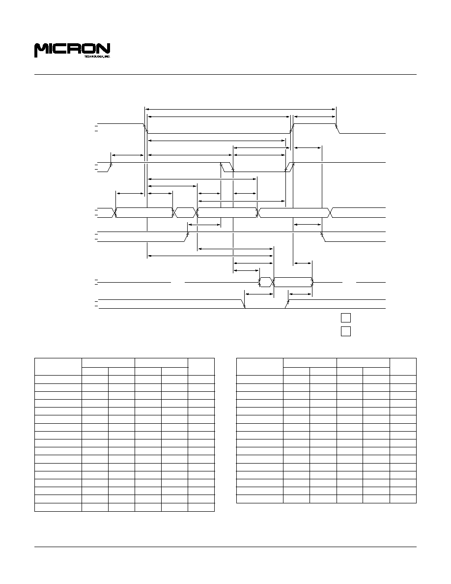
READ CYCLE
27
,,
,
,,
,,
,,,
,,
,
,
tRRH
,
,,,
,,
tCLZ
tCAC
tRAC
tAA
VALID DATA
OPEN
tOFF
tRCH
ROW
tRCS
tASC
tRAH
tRAD
tAR
tCAH
tRCD
tCAS
tRSH
tCSH
tRP
tRC
tRAS
tCRP
tASR
ROW
OPEN
RAS#
V
V
IH
IL
V
V
IH
IL
ADDR
V
V
IH
IL
DQ
V
V
OH
OL
V
V
IH
IL
,,,
,,,,
,,,
,,
t OD
t OE
OE#
V
V
IH
IL
COLUMN
,,,
,,,,
,,
CAS#
WE#
,,
,,,
,,,
NOTE 1
tACH
DON'T CARE
UNDEFINED
,
,
,
NOTE: 1. For EDO,
t
OFF is referenced from rising edge of RAS# or CAS#, whichever occurs last. For FPM,
t
OFF is referenced from rising edge of RAS# or
CAS#, whichever occurs first.
*EDO version only
t
OFF (EDO)
0
12
0
15
ns
t
OFF (FPM)
≠
≠
3
15
ns
t
RAC
50
60
ns
t
RAD (EDO)
9
12
ns
t
RAD (FPM)
≠
15
ns
t
RAH
9
10
ns
t
RAS
50
10,000
60
10,000
ns
t
RC (EDO)
84
104
ns
t
RC (FPM)
≠
110
ns
t
RCD (EDO)
11
14
ns
t
RCD (FPM)
≠
20
ns
t
RCH
0
0
ns
t
RCS
0
0
ns
t
RP
30
40
ns
t
RRH
0
0
ns
t
RSH
13
15
ns
-5*
-6
SYMBOL
MIN
MAX
MIN
MAX
UNITS
FAST PAGE MODE AND EDO PAGE MODE
TIMING PARAMETERS
-5*
-6
SYMBOL
MIN
MAX
MIN
MAX
UNITS
t
AA
25
30
ns
t
ACH (EDO)
12
15
ns
t
AR
38
45
ns
t
ASC
0
0
ns
t
ASR
0
0
ns
t
CAC
13
15
ns
t
CAH
8
10
ns
t
CAS (EDO)
8
10,000
10
10,000
ns
t
CAS (FPM)
≠
≠
15
10,000
ns
t
CLZ (EDO)
0
0
ns
t
CLZ (FPM)
≠
3
ns
t
CRP
5
5
ns
t
CSH (EDO)
38
45
ns
t
CSH (FPM)
≠
60
ns
t
OD (EDO)
0
12
0
15
ns
t
OD (FPM)
≠
≠
3
15
ns
t
OE
12
15
ns

2, 4 Meg x 72 Nonbuffered DRAM DIMMs
Micron Technology, Inc., reserves the right to change products or specifications without notice.
DM60.p65 ≠ Rev. 6/98
©
1998, Micron Technology, Inc.
18
2, 4 MEG x 72
NONBUFFERED DRAM DIMMs
OBSOLETE
EARLY WRITE CYCLE
27
DON'T CARE
UNDEFINED
,
,,
,,,
,,,
,,,
,,,
,,
,,
V
V
IH
IL
,,
,
,
,,,
,,
,,
,,,
,,,
,,
VALID DATA
ROW
COLUMN
ROW
tDS
tWP
tWCH
tWCS
tWCR
tRWL
tCWL
tCAH
tASC
tRAH
tASR
tRAD
tAR
tCAS
tRSH
tCSH
tRCD
tCRP
tRAS
tRC
tRP
V
V
IH
IL
ADDR
V
V
IH
IL
V
V
IH
IL
DQ
V
V
IOH
IOL
V
V
IH
IL
RAS#
OE#
,,
,,,
,,
,,,
,,,
,,,
,,,
,,,
,,
,,
,,,
,,,
,,,
tDH
WE#
CAS#
tACH
,,,
,,,
,,
*EDO version only
t
RAD (EDO)
9
12
ns
t
RAH
9
10
ns
t
RAS
50
10,000
60
10,000
ns
t
RC (FPM)
≠
110
ns
t
RC (EDO)
84
104
ns
t
RCD (FPM)
≠
20
ns
t
RCD (EDO)
11
14
ns
t
RP
30
40
ns
t
RSH
13
15
ns
t
RWL
13
15
ns
t
WCH
8
10
ns
t
WCR
38
45
ns
t
WCS
0
0
ns
t
WP (FPM)
≠
10
ns
t
WP (EDO)
5
5
ns
FAST PAGE MODE AND EDO PAGE MODE
TIMING PARAMETERS
-5*
-6
SYMBOL
MIN
MAX
MIN
MAX
UNITS
t
ACH (EDO)
12
15
ns
t
AR
38
45
ns
t
ASC
0
0
ns
t
ASR
0
0
ns
t
CAH
8
10
ns
t
CAS (FPM)
≠
≠
15
10,000
ns
t
CAS (EDO)
8
10,000
10
10,000
ns
t
CRP
5
5
ns
t
CSH (FPM)
≠
60
ns
t
CSH (EDO)
38
45
ns
t
CWL (FPM)
≠
15
ns
t
CWL (EDO)
8
10
ns
t
DH
8
10
ns
t
DS
0
0
ns
t
RAD (FPM)
≠
15
ns
-5*
-6
SYMBOL
MIN
MAX
MIN
MAX
UNITS
2, 4 Meg x 72 Nonbuffered DRAM DIMMs
Micron Technology, Inc., reserves the right to change products or specifications without notice.
DM60.p65 ≠ Rev. 6/98
©
1998, Micron Technology, Inc.
19
2, 4 MEG x 72
NONBUFFERED DRAM DIMMs
OBSOLETE
t
OE
15
ns
t
OFF
3
15
ns
t
PC
35
ns
t
RAC
60
ns
t
RAD
15
ns
t
RAH
10
ns
t
RASP
60
125,000
ns
t
RCD
20
ns
t
RCH
0
ns
t
RCS
0
ns
t
RP
40
ns
t
RRH
0
ns
t
RSH
15
ns
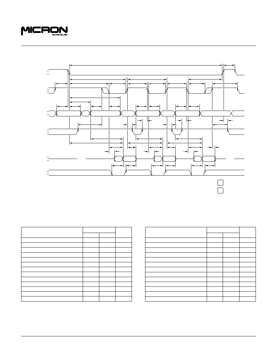
FAST-PAGE-MODE READ CYCLE
,
,,
,,
,
,
,,,
,,
,,
,,
,,
,,
,,
,,,
,,
,,,,
,,,
,
,,,
,,
,
,
VALID
DATA
,,
,,
VALID
DATA
,
,
VALID
DATA
,
,
,
,
,,
,
,
,,
,,,
,,
COLUMN
COLUMN
COLUMN
ROW
ROW
tRCS
tCAH
tASC
tCP
tCAS
tRSH
tCP
tCAS
tCP
tCAS
tRCD
tCRP
tPC
tCSH
tRASP
tRP
tCAH
tASC
tCAH
tASC
tAR
tRAH
tRAD
tASR
tRCS
tRCH
tRCH
tRCS
tRRH
tRCH
tOFF
tCAC
tCPA
tAA
tCLZ
tOFF
tCAC
tCPA
tAA
tCLZ
tOFF
tCAC
tRAC
tAA
tCLZ
tOE
tOD
tOE
tOD
tOE
tOD
OPEN
OPEN
V
V
IH
IL
CAS#
V
V
IH
IL
ADDR
V
V
IH
IL
WE#
V
V
IH
IL
DQ
V
V
IOH
IOL
V
V
IH
IL
RAS#
OE#
DON'T CARE
UNDEFINED
,
,
,
FAST PAGE MODE
TIMING PARAMETERS
-6
SYMBOL
MIN
MAX
UNITS
t
AA
30
ns
t
AR
45
ns
t
ASC
0
ns
t
ASR
0
ns
t
CAC
15
ns
t
CAH
10
ns
t
CAS
15
10,000
ns
t
CLZ
3
ns
t
CP
10
ns
t
CPA
35
ns
t
CRP
5
ns
t
CSH
60
ns
t
OD
3
15
ns
-6
SYMBOL
MIN
MAX
UNITS

2, 4 Meg x 72 Nonbuffered DRAM DIMMs
Micron Technology, Inc., reserves the right to change products or specifications without notice.
DM60.p65 ≠ Rev. 6/98
©
1998, Micron Technology, Inc.
20
2, 4 MEG x 72
NONBUFFERED DRAM DIMMs
OBSOLETE
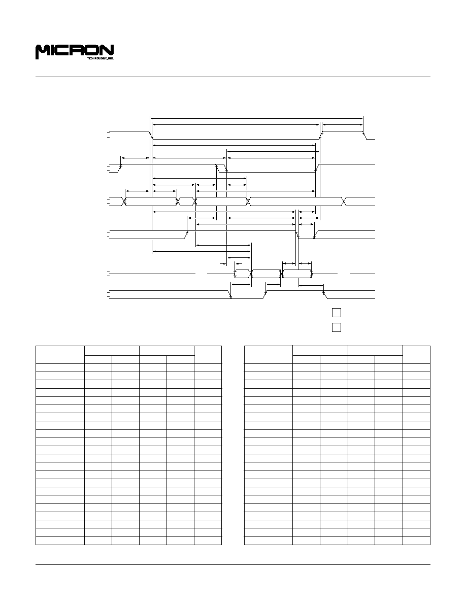
EDO-PAGE-MODE READ CYCLE
,
,
,,,
,,,
,,,
,,,
,,
,
,
VALID
DATA
,,
,,
VALID
DATA
,
,
VALID
DATA
,,
,
,,
,
,,
,,
,
,,
,,,
,
COLUMN
COLUMN
COLUMN
ROW
ROW
DON'T CARE
UNDEFINED
,,
,
tOD
tCAH
tASC
tCP
tRSH
tCP
tCP
tCAS
tRCD
tCRP
tPC
tCSH
tRASP
tRP
tCAH
tASC
tCAH
tASC
tAR
tRAH
tRAD
tASR
tRCS
tRRH
tRCH
tOFF
tCAC
tCPA
tAA
tCLZ
tCAC
tCPA
tAA
tCAC
tRAC
tAA
tCLZ
tOE
tOD
tOE
tOD
OPEN
OPEN
V
V
IH
IL
V
V
IH
IL
ADDR
V
V
IH
IL
V
V
IH
IL
DQ
V
V
OH
OL
V
V
IH
IL
RAS#
OE#
tCAS
tCAS
CAS#
WE#
tCOH
tOEP
tOEHC
tOES
tOES
tACH
tACH
tACH
,,
,,,,
,,
-5
-6
SYMBOL
MIN
MAX
MIN
MAX
UNITS
t
OEHC
5
10
ns
t
OEP
5
5
ns
t
OES
4
5
ns
t
OFF
0
12
0
15
ns
t
PC
20
25
ns
t
RAC
50
60
ns
t
RAD
9
12
ns
t
RAH
9
10
ns
t
RASP
50
125,000
60
125,000
ns
t
RCD
11
14
ns
t
RCH
0
0
ns
t
RCS
0
0
ns
t
RP
30
40
ns
t
RRH
0
0
ns
t
RSH
13
15
ns
EDO PAGE MODE
TIMING PARAMETERS
-5
-6
SYMBOL
MIN
MAX
MIN
MAX
UNITS
t
AA
25
30
ns
t
ACH
12
15
ns
t
AR
38
45
ns
t
ASC
0
0
ns
t
ASR
0
0
ns
t
CAC
13
15
ns
t
CAH
8
10
ns
t
CAS
8
10,000
10
10,000
ns
t
CLZ
0
0
ns
t
COH
3
3
ns
t
CP
8
10
ns
t
CPA
28
35
ns
t
CRP
5
5
ns
t
CSH
38
45
ns
t
OD
0
12
0
15
ns
t
OE
12
15
ns

2, 4 Meg x 72 Nonbuffered DRAM DIMMs
Micron Technology, Inc., reserves the right to change products or specifications without notice.
DM60.p65 ≠ Rev. 6/98
©
1998, Micron Technology, Inc.
21
2, 4 MEG x 72
NONBUFFERED DRAM DIMMs
OBSOLETE
FAST/EDO-PAGE-MODE EARLY WRITE CYCLE
27
,,
,,,
,
,,
,,
,,
,,
,,
,
,,
,,
,
,
,,
,
,,
,
,,,
,,
,,
,
,
,,
,,,
,,,
,
tDS
tDH
tDS
tDH
tDS
tDH
tWCR
VALID DATA
VALID DATA
VALID DATA
tRWL
tWP
tCWL
tWCH
tWCS
tWP
tCWL
tWCH
tWCS
tWP
tCWL
tWCH
tWCS
tCAH
tASC
tCAH
tASC
tCAH
tASC
tRAH
tASR
tRAD
tACH
tACH
tACH
tAR
COLUMN
COLUMN
COLUMN
ROW
ROW
tCP
tCAS
tRSH
tCP
tCAS
tCP
tCAS
tRCD
tCRP
tPC
tCSH
tRASP
tRP
V
V
IH
IL
CAS#
V
V
IH
IL
ADDR
V
V
IH
IL
WE#
V
V
IH
IL
DQ
V
V
IOH
IOL
RAS#
OE#
V
V
IH
IL
,,,
,,,
,,,
,,,,
,,,,
,,,
,,,
,,
DON'T CARE
UNDEFINED
,
,
,
,
,
,,,
,,
*EDO version only
-5*
-6
SYMBOL
MIN
MAX
MIN
MAX
UNITS
t
PC (FPM)
≠
35
ns
t
RAD (EDO)
9
12
ns
t
RAD (FPM)
≠
15
ns
t
RAH
9
10
ns
t
RASP
50
125,000
60
125,000
ns
t
RCD (EDO)
11
14
ns
t
RCD (FPM)
≠
20
ns
t
RP
30
40
ns
t
RSH
13
15
ns
t
RWL
13
15
ns
t
WCH
8
10
ns
t
WCR
38
45
ns
t
WCS
0
0
ns
t
WP (EDO)
5
5
ns
t
WP (FPM)
≠
10
ns
FAST PAGE MODE AND EDO PAGE MODE
TIMING PARAMETERS
-5*
-6
SYMBOL
MIN
MAX
MIN
MAX
UNITS
t
ACH (EDO)
12
15
ns
t
AR
38
45
ns
t
ASC
0
0
ns
t
ASR
0
0
ns
t
CAH
8
10
ns
t
CAS (EDO)
8
10,000
10
10,000
ns
t
CAS (FPM)
≠
≠
15
10,000
ns
t
CP
8
10
ns
t
CRP
5
5
ns
t
CSH (EDO)
38
45
ns
t
CSH (FPM)
≠
60
ns
t
CWL (EDO)
8
10
ns
t
CWL (FPM)
≠
15
ns
t
DH
8
10
ns
t
DS
0
0
ns
t
PC (EDO)
20
25
ns
2, 4 Meg x 72 Nonbuffered DRAM DIMMs
Micron Technology, Inc., reserves the right to change products or specifications without notice.
DM60.p65 ≠ Rev. 6/98
©
1998, Micron Technology, Inc.
22
2, 4 MEG x 72
NONBUFFERED DRAM DIMMs
OBSOLETE
READ-WRITE CYCLE
27
(LATE WRITE and READ-MODIFY-WRITE cycles)
,,,
,,,
,
,
,
VALID D
OUT
VALID D
IN
,,
,,
,,
,,
ROW
,,,
,,,
,,
COLUMN
ROW
,,
,,,
,,,
,,,,
,
V
V
IH
IL
V
V
IH
IL
ADDR
V
V
IH
IL
V
V
IH
IL
DQ
V
V
IOH
IOL
V
V
IH
IL
RAS#
OPEN
OPEN
tOE
tOD
tCAC
tRAC
tAA
tCLZ
tDS
tDH
tAWD
tWP
tRWL
tCWL
tCWD
tRWD
tRCS
tASC
tCAH
tAR
tASR
tRAD
tCRP
tRCD
tCAS
tRSH
tCSH
tRAS
tRWC
tRP
tRAH
OE#
tOEH
,
,,,
,,,
WE#
tACH
CAS#
,,
,
,
DON'T CARE
UNDEFINED
,,
,,,,
,,
-5*
-6
SYMBOL
MIN
MAX
MIN
MAX
UNITS
t
OD (EDO)
0
12
0
15
ns
t
OD (FPM)
≠
≠
3
15
ns
t
OE
12
15
ns
t
OEH (EDO)
8
10/12**
ns
t
OEH (FPM)
≠
15
ns
t
RAC
50
60
ns
t
RAD (EDO)
9
12
ns
t
RAD (FPM)
≠
15
ns
t
RAH
9
10
ns
t
RAS
50
10,000
60
10,000
ns
t
RCD (EDO)
11
14
ns
t
RCD (FPM)
≠
20
ns
t
RCS
0
0
ns
t
RP
30
40
ns
t
RSH
13
15
ns
t
RWC (EDO)
116
140
ns
t
RWC (FPM)
≠
155
ns
t
RWD (EDO)
67
79
ns
t
RWD (FPM)
≠
85
ns
t
RWL
13
15
ns
t
WP (EDO)
5
5
ns
t
WP (FPM)
≠
10
ns
FAST PAGE MODE AND EDO PAGE MODE
TIMING PARAMETERS
-5*
-6
SYMBOL
MIN
MAX
MIN
MAX
UNITS
t
AA
25
30
ns
t
ACH (EDO)
12
15
ns
t
AR
38
45
ns
t
ASC
0
0
ns
t
ASR
0
0
ns
t
AWD (EDO)
42
49
ns
t
AWD (FPM)
≠
55
ns
t
CAC
13
15
ns
t
CAH
8
10
ns
t
CAS (EDO)
8
10,000
10
10,000
ns
t
CAS (FPM)
≠
≠
15
10,000
ns
t
CLZ (EDO)
0
0
ns
t
CLZ (FPM)
≠
3
ns
t
CRP
5
5
ns
t
CSH (EDO)
38
45
ns
t
CSH (FPM)
≠
60
ns
t
CWD (EDO)
28
35
ns
t
CWD (FPM)
≠
40
ns
t
CWL (EDO)
8
10
ns
t
CWL (FPM)
≠
15
ns
t
DH
8
10
ns
t
DS
0
0
ns
* EDO version only
**16MB DIMM

2, 4 Meg x 72 Nonbuffered DRAM DIMMs
Micron Technology, Inc., reserves the right to change products or specifications without notice.
DM60.p65 ≠ Rev. 6/98
©
1998, Micron Technology, Inc.
23
2, 4 MEG x 72
NONBUFFERED DRAM DIMMs
OBSOLETE
NOTE: 1.
t
PC is for LATE WRITE cycles only.
FAST/EDO-PAGE-MODE READ-WRITE CYCLE
27
(LATE WRITE and READ-MODIFY-WRITE cycles)
* EDO version only
**16MB DIMM
,,
,,,
,,,,
,
,,
,,
,,
,,
,
,
,
,
,,
,,
,,
,,
,,
,,,
,
DON'T CARE
UNDEFINED
,,
,,
,
,,
,,
tOE
tOE
tOE
OPEN
D OUT
VALID
DIN
VALID
D OUT
VALID
D IN
VALID
D OUT
VALID
D IN
VALID
OPEN
tDH
tDS
tAA
tCPA
tCLZ
tCAC
tDH
tDS
tAA
tCPA
tCLZ
tCAC
tDH
tDS
tAA
tCLZ
tCAC
tRAC
tWP
tCWL
tRWL
tCWD
tAWD
tWP
tCWL
tCWD
tAWD
tWP
tCWL
tCWD
tAWD
tRCS
tRWD
tASR
tRAH
tASC
tRAD
tAR
tCAH
tASC
tCAH
tASC
tCAH
tCP
tCAS
tRSH
tCP
tRP
tRASP
tCAS
tCP
tCAS
tRCD
tCSH
tPC
tCRP
ROW
COLUMN
COLUMN
COLUMN
ROW
V
V
IH
IL
CAS#
V
V
IH
IL
ADDR
V
V
IH
IL
V
V
IH
IL
DQ
V
V
IOH
IOL
V
V
IH
IL
RAS#
OE#
WE#
tPRWC
,
,,,
tOEH
tOD
tOD
tOD
NOTE 1
,,
,,,
,
-5*
-6
SYMBOL
MIN
MAX
MIN
MAX
UNITS
t
OD (FPM)
≠
≠
3
15
ns
t
OE
12
15
ns
t
OEH (EDO)
8
10/12**
ns
t
OEH (FPM)
≠
15
ns
t
PC (EDO)
20
25
ns
t
PC (FPM)
≠
35
ns
t
PRWC (EDO)
47
56
ns
t
PRWC (FPM)
≠
85
ns
t
RAC
50
60
ns
t
RAD (EDO)
9
12
ns
t
RAD (FPM)
≠
15
ns
t
RAH
9
10
ns
t
RASP
50
125,000
60
125,000
ns
t
RCD (EDO)
11
14
ns
t
RCD (FPM)
≠
20
ns
t
RCS
0
0
ns
t
RP
30
40
ns
t
RSH
13
15
ns
t
RWD (EDO)
67
79
ns
t
RWD (FPM)
≠
85
ns
t
RWL
13
15
ns
t
WP (EDO)
5
5
ns
t
WP (FPM)
≠
10
ns
FAST PAGE MODE AND EDO PAGE MODE
TIMING PARAMETERS
-5*
-6
SYMBOL
MIN
MAX
MIN
MAX
UNITS
t
AA
25
30
ns
t
AR
38
45
ns
t
ASC
0
0
ns
t
ASR
0
0
ns
t
AWD (EDO)
42
49
ns
t
AWD (FPM)
≠
55
ns
t
CAC
13
15
ns
t
CAH
8
10
ns
t
CAS (EDO)
8
10,000
10
10,000
ns
t
CAS (FPM)
≠
≠
15
10,000
ns
t
CLZ (EDO)
0
0
ns
t
CLZ (FPM)
≠
3
ns
t
CP
8
10
ns
t
CPA
28
35
ns
t
CRP
5
5
ns
t
CSH (EDO)
38
45
ns
t
CSH (FPM)
≠
60
ns
t
CWD (EDO)
28
35
ns
t
CWD (FPM)
≠
40
ns
t
CWL (EDO)
8
10
ns
t
CWL (FPM)
≠
15
ns
t
DH
8
10
ns
t
DS
0
0
ns
t
OD (EDO)
0
12
0
15
ns

2, 4 Meg x 72 Nonbuffered DRAM DIMMs
Micron Technology, Inc., reserves the right to change products or specifications without notice.
DM60.p65 ≠ Rev. 6/98
©
1998, Micron Technology, Inc.
24
2, 4 MEG x 72
NONBUFFERED DRAM DIMMs
OBSOLETE
EDO-PAGE-MODE READ EARLY WRITE CYCLE
(Pseudo READ-MODIFY-WRITE)
V
V
IH
IL
V
V
IH
IL
RAS#
V
V
IH
IL
ADDR
V
V
IH
IL
WE#
,,
t RASP
t RP
ROW
,,
COLUMN (A)
,,
,
COLUMN (N)
,,
,,
ROW
V
V
IH
IL
OE#
V
V
IOH
IOL
tCRP
t CSH
t CAS
t RCD
tASR
t RAH
tRAD
t ASC
tAR
t CAH
t ASC
t CAH
t ASC
t CAH
t CP
t RSH
VALID DATA
IN
,,,
,,,,
,,
,
,,
,
t RCS
t RCH
t WCS
tOE
VALID
DATA (B)
VALID DATA (A)
t WHZ
tCAC
tCPA
tAA
tCAC
tAA
OPEN
DQ
tPC
RAC
t
tCOH
t WCH
t DS
t DH
tPC
COLUMN (B)
t ACH
CAS#
t CAS
t CAS
t CP
t CP
DON'T CARE
UNDEFINED
,,
,
,,
,,,
,
-5
-6
SYMBOL
MIN
MAX
MIN
MAX
UNITS
t
OE
12
15
ns
t
PC
20
25
ns
t
RAC
50
60
ns
t
RAD
9
12
ns
t
RAH
9
10
ns
t
RASP
50
125,000
60
125,000
ns
t
RCD
11
14
ns
t
RCH
0
0
ns
t
RCS
0
0
ns
t
RP
30
40
ns
t
RSH
13
15
ns
t
WCH
8
10
ns
t
WCS
0
0
ns
t
WHZ
0
12
0
15
ns
EDO PAGE MODE
TIMING PARAMETERS
-5
-6
SYMBOL
MIN
MAX
MIN
MAX
UNITS
t
AA
25
30
ns
t
ACH
12
15
ns
t
AR
38
45
ns
t
ASC
0
0
ns
t
ASR
0
0
ns
t
CAC
13
15
ns
t
CAH
8
10
ns
t
CAS
8
10,000
10
10,000
ns
t
COH
3
3
ns
t
CP
8
10
ns
t
CPA
28
35
ns
t
CRP
5
5
ns
t
CSH
38
45
ns
t
DH
8
10
ns
t
DS
0
0
ns

2, 4 Meg x 72 Nonbuffered DRAM DIMMs
Micron Technology, Inc., reserves the right to change products or specifications without notice.
DM60.p65 ≠ Rev. 6/98
©
1998, Micron Technology, Inc.
25
2, 4 MEG x 72
NONBUFFERED DRAM DIMMs
OBSOLETE
,,
,,
ROW
VALID
DATA
,
,
VALID DATA
,,
,,,
,,
OPEN
tCRP
tRCD
tCAS
tRSH
tRASP
tRP
tPC
tASC
tCAH
tAR
tASR
tRAD
tRAH
tWCS
tWP
tRWL
tRCS
tDH
tDS
tCAC
t OFF
V
V
IH
IL
CAS#
V
V
IH
IL
ADDR
V
V
IH
IL
RAS#
DQ
V
V
OH
OL
WE#
V
V
IH
IL
,,
,,,
,,,
tCSH
,
,,
,,,
,,
COLUMN
tCP
tCP
tASC
tCAH
tCWL
tWCH
t CLZ
tAA
RAC
DON'T CARE
UNDEFINED
,
,
,
t
NOTE 1
,,
,,
OE#
V
V
IH
IL
ROW
COLUMN
tCAS
FAST-PAGE-MODE READ EARLY WRITE CYCLE
(Pseudo READ-MODIFY-WRITE)
NOTE: 1. Do not drive data prior to tristate.
-6
SYMBOL
MIN
MAX
UNITS
t
OFF
3
15
ns
t
PC
35
ns
t
RAC
60
ns
t
RAD
15
ns
t
RAH
10
ns
t
RASP
60
125,000
ns
t
RCD
20
ns
t
RCS
0
ns
t
RP
40
ns
t
RSH
15
ns
t
RWL
15
ns
t
WCH
10
ns
t
WCS
0
ns
t
WP
10
ns
FAST PAGE MODE
TIMING PARAMETERS
-6
SYMBOL
MIN
MAX
UNITS
t
AA
30
ns
t
AR
45
ns
t
ASC
0
ns
t
ASR
0
ns
t
CAC
15
ns
t
CAH
10
ns
t
CAS
15
10,000
ns
t
CLZ
3
ns
t
CP
10
ns
t
CRP
5
ns
t
CSH
60
ns
t
CWL
15
ns
t
DH
10
ns
t
DS
0
ns

2, 4 Meg x 72 Nonbuffered DRAM DIMMs
Micron Technology, Inc., reserves the right to change products or specifications without notice.
DM60.p65 ≠ Rev. 6/98
©
1998, Micron Technology, Inc.
26
2, 4 MEG x 72
NONBUFFERED DRAM DIMMs
OBSOLETE
EDO READ CYCLE
(with WE#-controlled disable)
,,
,
,,
,
,
,
,,,
,,
tCLZ
tCAC
tRAC
tAA
VALID DATA
OPEN
tRCH
tRCS
tASC
tRAH
tRAD
tAR
tCAH
tRCD
tCAS
tCSH
tCRP
tASR
ROW
OPEN
RAS#
V
V
IH
IL
V
V
IH
IL
ADDR
V
V
IH
IL
DQ
V
V
OH
OL
V
V
IH
IL
,,,
,,,,
,,,
,,
t OD
t OE
OE#
V
V
IH
IL
COLUMN
,,,
,,,,
,
WE#
tWHZ
tWPZ
tCP
tASC
tRCS
COLUMN
,
tCLZ
DON'T CARE
UNDEFINED
,,
,
CAS#
,,
,,,
,,,
-5
-6
SYMBOL
MIN
MAX
MIN
MAX
UNITS
EDO PAGE MODE
TIMING PARAMETERS
-5
-6
SYMBOL
MIN
MAX
MIN
MAX
UNITS
t
AA
25
30
ns
t
AR
38
45
ns
t
ASC
0
0
ns
t
ASR
0
0
ns
t
CAC
13
15
ns
t
CAH
8
10
ns
t
CAS
8
10,000
10
10,000
ns
t
CLZ
0
0
ns
t
CP
8
10
ns
t
CRP
5
5
ns
t
CSH
38
45
ns
t
OD
0
12
0
15
ns
t
OE
12
15
ns
t
RAC
50
60
ns
t
RAD
9
12
ns
t
RAH
9
10
ns
t
RCD
11
14
ns
t
RCH
0
0
ns
t
RCS
0
0
ns
t
WHZ
0
12
0
15
ns
t
WPZ
10
10
ns

2, 4 Meg x 72 Nonbuffered DRAM DIMMs
Micron Technology, Inc., reserves the right to change products or specifications without notice.
DM60.p65 ≠ Rev. 6/98
©
1998, Micron Technology, Inc.
27
2, 4 MEG x 72
NONBUFFERED DRAM DIMMs
OBSOLETE
RAS#-ONLY REFRESH CYCLE
27
,,,
,,,,
,,,
,
,,
,
ROW
V
V
IH
IL
CAS#
V
V
IH
IL
ADDR
V
V
IH
IL
RAS#
tRC
tRAS
tRP
tCRP
tASR
tRAH
ROW
OPEN
DQ
V
V
OH
OL
tRPC
WE#
V
V
IH
IL
,
,,,
,,,,
,,,
,,,,
,,,,
,,,,
,,
*EDO version only
CBR REFRESH CYCLE
27
(Addresses, OE# = DON'T CARE)
tRP
V
V
IH
IL
RAS#
tRAS
NOTE 1
OPEN
tCHR
tCSR
V
V
IH
IL
V
V
OH
OL
CAS#
DQ
tRP
tRAS
tRPC
tCSR
tRPC
tCHR
tCP
V
V
IH
IL
tWRP
tWRH
,
,,,
,,,
,
,,,
,,
,,
,,,
,,
WE#
tWRP
tWRH
DON'T CARE
UNDEFINED
,,
,,
,
-5*
-6
SYMBOL
MIN
MAX
MIN
MAX
UNITS
t
RC (FPM)
≠
110
ns
t
RC (EDO)
84
104
ns
t
RP
30
40
ns
t
RPC (FPM)
≠
0
ns
t
RPC (EDO)
5
5
ns
t
WRH
8
10
ns
t
WRP
8
10
ns
FAST PAGE MODE AND EDO PAGE MODE
TIMING PARAMETERS
-5*
-6
SYMBOL
MIN
MAX
MIN
MAX
UNITS
t
ASR
0
0
ns
t
CHR
8
10
ns
t
CP
8
10
ns
t
CRP
5
5
ns
t
CSR
5
5
ns
t
RAH
9
10
ns
t
RAS
50
10,000
60
10,000
ns

2, 4 Meg x 72 Nonbuffered DRAM DIMMs
Micron Technology, Inc., reserves the right to change products or specifications without notice.
DM60.p65 ≠ Rev. 6/98
©
1998, Micron Technology, Inc.
28
2, 4 MEG x 72
NONBUFFERED DRAM DIMMs
OBSOLETE
HIDDEN REFRESH CYCLE
20, 27
(WE# = HIGH; OE# = LOW)
,,,
,,
,,
,,
DON'T CARE
UNDEFINED
,
,,
tCLZ
tOFF
,,,
,,,
,,,
,,,
,,
,,
,,
,,
,,
OPEN
VALID DATA
OPEN
COLUMN
ROW
tCAC
tRAC
tAA
tCAH
tASC
tRAH
tASR
tRAD
tAR
tCRP
tRCD
tRSH
tRAS
tRC
tRP
tCHR
tRAS
DQ
V
V
IOH
IOL
V
V
IH
IL
ADDR
V
V
IH
IL
CAS#
V
V
IH
IL
RAS#
,,,
,,,,
,,,
V
V
IH
IL
tOE
tOD
OE#
tORD
FAST PAGE MODE AND EDO PAGE MODE
TIMING PARAMETERS
-5*
-6
SYMBOL
MIN
MAX
MIN
MAX
UNITS
t
AA
25
30
ns
t
AR
38
45
ns
t
ASC
0
0
ns
t
ASR
0
0
ns
t
CAC
13
15
ns
t
CAH
8
10
ns
t
CHR
8
10
ns
t
CLZ (FPM)
≠
3
ns
t
CLZ (EDO)
0
0
ns
t
CRP
5
5
ns
t
OD (FPM)
≠
≠
3
15
ns
t
OD (EDO)
0
12
0
15
ns
t
OE
12
15
ns
t
OFF (FPM)
≠
≠
3
15
ns
-5*
-6
SYMBOL
MIN
MAX
MIN
MAX
UNITS
t
OFF (EDO)
0
12
0
15
ns
t
ORD
0
0
ns
t
RAC
50
60
ns
t
RAD (FPM)
≠
15
ns
t
RAD (EDO)
9
12
ns
t
RAH
9
10
ns
t
RAS
50
10,000
60
10,000
ns
t
RC (FPM)
≠
110
ns
t
RC (EDO)
84
104
ns
t
RCD (FPM)
≠
20
ns
t
RCD (EDO)
11
14
ns
t
RP
30
40
ns
t
RSH
13
15
ns
*EDO version only

2, 4 Meg x 72 Nonbuffered DRAM DIMMs
Micron Technology, Inc., reserves the right to change products or specifications without notice.
DM60.p65 ≠ Rev. 6/98
©
1998, Micron Technology, Inc.
29
2, 4 MEG x 72
NONBUFFERED DRAM DIMMs
OBSOLETE
,,,,,,
SCL
SDA IN
SDA OUT
tLOW
t SU:STA
t HD:STA
tF
tHIGH
tR
tBUF
tDH
tAA
t SU:STO
t SU:DAT
t HD:DAT
UNDEFINED
,
SERIAL PRESENCE-DETECT EEPROM
TIMING PARAMETERS
SYMBOL
MIN
MAX
UNITS
t
AA
0.3
3.5
µ
s
t
BUF
4.7
µ
s
t
DH
300
ns
t
F
300
ns
t
HD:DAT
0
µ
s
t
HD:STA
4
µ
s
SPD EEPROM
t
HIGH
4
µ
s
t
LOW
4.7
µ
s
t
R
1
µ
s
t
SU:DAT
250
ns
t
SU:STA
4.7
µ
s
t
SU:STO
4.7
µ
s
SYMBOL
MIN
MAX
UNITS
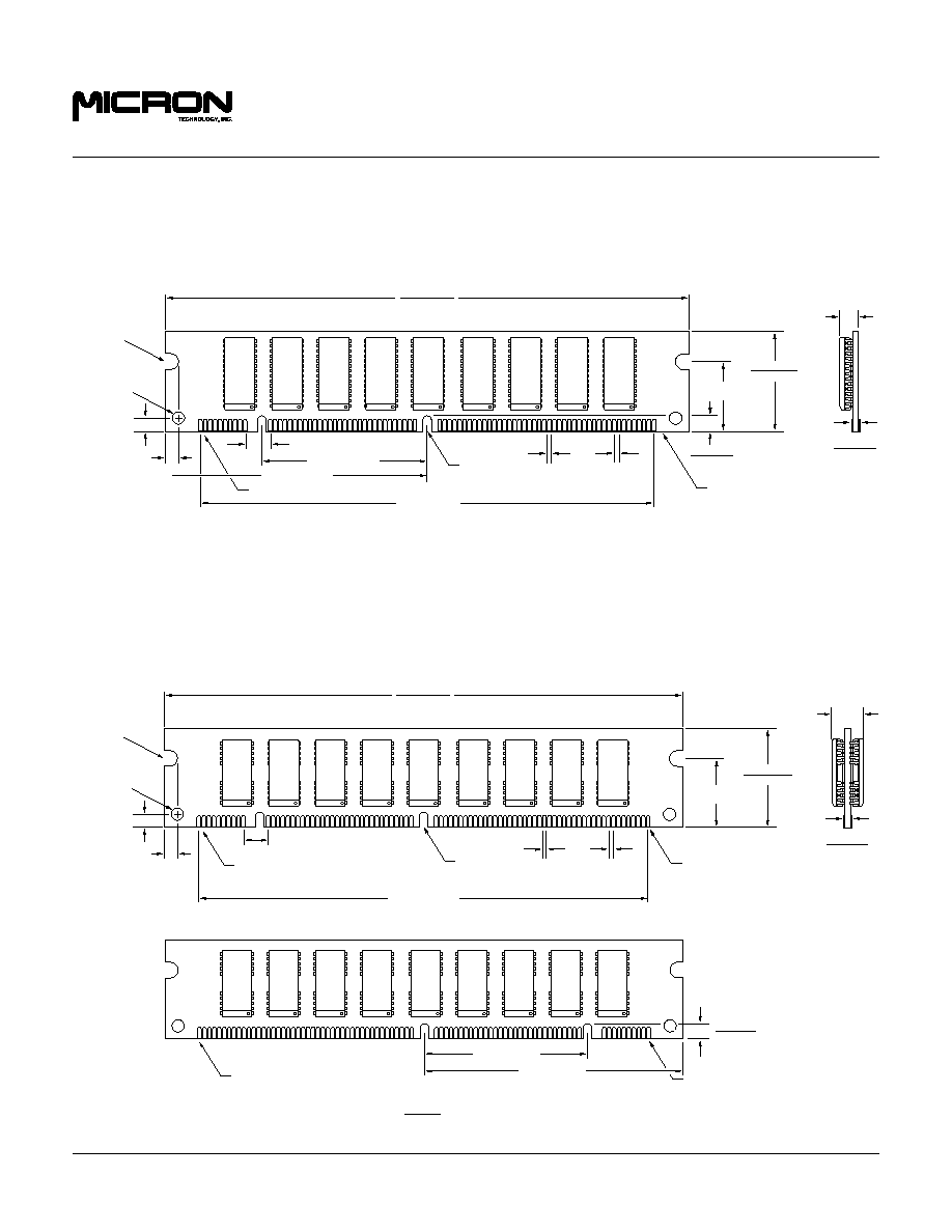
2, 4 Meg x 72 Nonbuffered DRAM DIMMs
Micron Technology, Inc., reserves the right to change products or specifications without notice.
DM60.p65 ≠ Rev. 6/98
©
1998, Micron Technology, Inc.
30
2, 4 MEG x 72
NONBUFFERED DRAM DIMMs
OBSOLETE
NOTE:
1. All dimensions in inches (millimeters)
MAX
or typical where noted.
MIN
168-PIN DIMM
DF-12 (16MB)
.200 (5.08)
MAX
.054 (1.37)
.046 (1.17)
1.005 (25.53)
.995 (25.27)
PIN 1 (PIN 85 on backside)
.700 (17.78)
TYP
.118 (3.00)
(2X)
.118 (3.00) TYP
4.550 (115.57)
.050 (1.27)
TYP
.118 (3.00)
TYP
.039 (1.00)
TYP
.079 (2.00) R
(2X)
.039 (1.00) R(2X)
FRONT VIEW
.128 (3.25)
.118 (3.00)
PIN 84 (PIN 168 ON BACKSIDE)
(2X)
.250 (6.35) TYP
1.661 (42.18)
2.625 (66.68)
5.256 (133.50)
5.244 (133.20)
168-PIN DIMM
DF-13 (32MB)
.350 (8.89)
MAX
.054 (1.37)
.046 (1.17)
PIN 1
.700 (17.78)
TYP
.118 (3.00)
(2X)
.118 (3.00) TYP
.250 (6.35) TYP
4.550 (115.57)
.050 (1.27)
TYP
.118 (3.00)
TYP
.039 (1.00)
TYP
.079 (2.00) R
(2X)
.039 (1.00) R(2X)
PIN 84
FRONT VIEW
BACK VIEW
PIN 168
.128 (3.25)
.118 (3.00)
(2X)
PIN 85
2.625 (66.68)
1.661 (42.18)
1.005 (25.53)
.995 (25.27)
5.256 (133.50)
5.244 (133.20)