Document Outline
- Features
- Options
- Key Timing Parameters
- Pin Assignment (Front View)
- Part Numbers
- General Description
- Fast Page Mode
- EDO Page Mode
- Refresh
- Functional Block Diagrams
- MT9LD272(X) (16MB)
- MT18LD472(F)(X) (32MB)
- Pin Descriptions
- Presence-Detect Truth Table
- Absolute Maximum Ratings
- DC Electrical Characteristics and Operating Conditions
- 2,048-Cycle Refresh ICC Operating Conditions and Maximum Limits
- 4,096-Cycle Refresh ICC Operating Conditions and Maximum Limits
- Capacitance
- Fast Page Mode AC Electrical Characteristics
- Fast Page Mode AC Electrical Characteristics
- EDO Page Mode AC Electrical Characteristics
- EDO Page Mode AC Electrical Characteristics
- Notes
- Read Cycle
- Early Write Cycle
- Fast-Page-Mode Read Cycle
- EDO-Page-Mode Read Cycle
- Fast/EDO-Page-Mode Early Write Cycle
- Read-Write Cycle
- Fast/EDO-Page-Mode Read-Write Cycle
- EDO-Page-Mode Read Early Write Cycle
- Fast-Page-Mode Read Early Write Cycle
- EDO Read Cycle
- RAS#-Only Refresh Cycle
- CBR Refresh Cycle
- Presence-Detect Read Cycle
- Hidden Refresh Cycle
- 168-Pin DIMMs
2, 4 Meg x 72 Buffered DRAM DIMMs
Micron Technology, Inc., reserves the right to change products or specifications without notice.
DM33.p65 ≠ Rev. 2/99
©1999, Micron Technology, Inc.
1
2, 4 MEG x 72
BUFFERED DRAM DIMMs
OBSOLETE
DRAM
MODULE
MT9LD272(X), MT18LD472(F)(X)
For the latest data sheet, please refer to the Micron Web
site:
www.micronsemi.com/datasheets/datasheet.html
PIN ASSIGNMENT (Front View)
PIN
SYMBOL
PIN
SYMBOL
PIN
SYMBOL
PIN
SYMBOL
1
V
SS
43
V
SS
85
V
SS
127
V
SS
2
DQ0
44
OE2#
86
DQ36
128
RFU
3
DQ1
45
RAS2#
87
DQ37
129
NC
4
DQ2
46
CAS4#
88
DQ38
130
NC
5
DQ3
47
RFU
89
DQ39
131
RFU
6
V
DD
48
WE2#
90
V
DD
132
PDE#
7
DQ4
49
V
DD
91
DQ40
133
V
DD
8
DQ5
50
NC
92
DQ41
134
NC
9
DQ6
51
NC
93
DQ42
135
NC
10
DQ7
52
DQ18
94
DQ43
136
DQ54
11
DQ8
53
DQ19
95
DQ44
137
DQ55
12
V
SS
54
V
SS
96
V
SS
138
V
SS
13
DQ9
55
DQ20
97
DQ45
139
DQ56
14
DQ10
56
DQ21
98
DQ46
140
DQ57
15
DQ11
57
DQ22
99
DQ47
141
DQ58
16
DQ12
58
DQ23
100
DQ48
142
DQ59
17
DQ13
59
V
DD
101
DQ49
143
V
DD
18
V
DD
60
DQ24
102
V
DD
144
DQ60
19
DQ14
61
RFU
103
DQ50
145
RFU
20
DQ15
62
RFU
104
DQ51
146
RFU
21
DQ16
63
RFU
105
DQ52
147
RFU
22
DQ17
64
RFU
106
DQ53
148
RFU
23
V
SS
65
DQ25
107
V
SS
149
DQ61
24
NC
66
DQ26
108
NC
150
DQ62
25
NC
67
DQ27
109
NC
151
DQ63
26
V
DD
68
V
SS
110
V
DD
152
V
SS
27
WE0#
69
DQ28
111
RFU
153
DQ64
28
CAS0#
70
DQ29
112
NC
154
DQ65
29
RFU
71
DQ30
113
RFU
155
DQ66
30
RAS0#
72
DQ31
114
NC
156
DQ67
31
OE0#
73
V
DD
115
RFU
157
V
DD
32
V
SS
74
DQ32
116
V
SS
158
DQ68
33
A0
75
DQ33
117
A1
159
DQ69
34
A2
76
DQ34
118
A3
160
DQ70
35
A4
77
DQ35
119
A5
161
DQ71
36
A6
78
V
SS
120
A7
162
V
SS
37
A8
79
PD1
121
A9
163
PD2
38
A10
80
PD3
122
A11
164
PD4
39
NC (A12)
81
PD5
123
NC (A13)
165
PD6
40
V
DD
82
PD7
124
V
DD
166
PD8
41
RFU
83
ID0
125
RFU
167
ID1
42
RFU
84
V
DD
126
B0
168
V
DD
FEATURES
∑ JEDEC-standard ECC pinout in a 168-pin, dual in-
line memory module (DIMM)
∑ 16MB (2 Meg x 72) and 32MB (4 Meg x 72)
∑ High-performance CMOS silicon-gate process
∑ Single +3.3V ±0.3V power supply
∑ All inputs, outputs and clocks are TTL-compatible
∑ Refresh modes: RAS#-ONLY, CAS#-BEFORE- RAS#
(CBR) and HIDDEN
∑ All inputs are buffered except RAS#
∑ 2,048 cycles (11 row, 11 column addresses) or
4,096 cycles (12 row, 10 column addresses)
∑ FAST-PAGE-MODE (FPM) or Extended Data-Out
(EDO) PAGE MODE access cycles
OPTIONS
MARKING
∑ Package
168-pin DIMM (gold)
G
∑ Timing
50ns access
-5*
60ns access
-6
∑ Access Cycles
FAST PAGE MODE
None
EDO PAGE MODE
X
∑ Refresh
2,048 cycles across 32ms
None
4,096 cycles across 64ms (32MB only)
F
* EDO version only
168-Pin DIMM
NOTE:
Pin symbols in parentheses are not used on these modules but
may be used for other modules in this product family. They are
for reference only.
KEY TIMING PARAMETERS
EDO Operating Mode
SPEED
t
RC
t
RAC
t
PC
t
AA
t
CAC
t
CAS
-5
84ns
50ns
20ns
30ns
18ns
8ns
-6
104ns
60ns
25ns
35ns
20ns
10ns
FPM Operating Mode
SPEED
t
RC
t
RAC
t
PC
t
AA
t
CAC
t
RP
-6
110ns
60ns
35ns
35ns
20ns
40ns
2, 4 Meg x 72 Buffered DRAM DIMMs
Micron Technology, Inc., reserves the right to change products or specifications without notice.
DM33.p65 ≠ Rev. 2/99
©1999, Micron Technology, Inc.
2
2, 4 MEG x 72
BUFFERED DRAM DIMMs
OBSOLETE
PART NUMBERS
EDO Operating Mode
PART NUMBER
CONFIGURATION REFRESH
MT9LD272G-x X
2 Meg x 72 ECC
2K Refresh
MT18LD472G-x X
4 Meg x 72 ECC
2K Refresh
MT18LD472FG-x X
4 Meg x 72 ECC
4K Refresh
x = speed
FPM Operating Mode
PART NUMBER
CONFIGURATION REFRESH
MT9LD272G-x
2 Meg x 72 ECC
2K Refresh
MT18LD472G-x
4 Meg x 72 ECC
2K Refresh
MT18LD472FG-x
4 Meg x 72 ECC
4K Refresh
x = speed
GENERAL DESCRIPTION
The MT9LD272(X) and MT18LD472(F)(X) are ran-
domly accessed 16MB and 32MB memories organized
in a x72 configuration. They are specially processed to
operate from 3V to 3.6V for low-voltage memory
systems.
During READ or WRITE cycles, each bit is uniquely
addressed through the address bits. Two copies of
address 0 (A0 and B0) are defined to allow maximum
performance for four-byte applications which inter-
leave between two four-byte banks. A0 is common to
the DRAMs used for DQ0-DQ35, while B0 is common
to the DRAMs used for DQ36-DQ71. RAS# is used to
latch the first 11/12 bits and CAS# the latter 10/11 bits.
READ and WRITE cycles are selected with the WE#
input. A logic HIGH on WE# dictates read mode, while
a logic LOW on WE# dictates write mode. During a
WRITE cycle, data-in (D) is latched by the falling edge
of WE# or CAS#, whichever occurs last. An EARLY
WRITE occurs when WE# is taken LOW prior to CAS#
falling. A LATE WRITE or READ-MODIFY-WRITE oc-
curs when WE# falls after CAS# was taken LOW.
During EARLY WRITE cycles, the data-outputs (Q) will
remain High-Z regardless of the state of OE#. During
LATE WRITE or READ-MODIFY-WRITE cycles, OE#
must be taken HIGH to disable the data-outputs prior
to applying input data. If a LATE WRITE or READ-
MODIFY-WRITE is attempted while keeping OE# LOW,
no WRITE will occur, and the data-outputs will drive
read data from the accessed location.
FAST PAGE MODE
FAST-PAGE-MODE operations allow faster data
operations (READ or WRITE) within a row-address-
defined page boundary. The FAST-PAGE-MODE cycle
is always initiated with a row address strobed in by
RAS#, followed by a column address strobed in by
CAS#. Additional columns may be accessed by provid-
ing valid column addresses, strobing CAS# and hold-
ing RAS# LOW, thus executing faster memory cycles.
Returning RAS# HIGH terminates the FAST-PAGE-
MODE operation.
EDO PAGE MODE
EDO PAGE MODE, designated by the "X" version,
is an accelerated FAST-PAGE-MODE cycle. The pri-
mary advantage of EDO is the availability of data-out
even after CAS# goes back HIGH. EDO provides for
CAS# precharge time (
t
CP) to occur without the out-
put data going invalid. This elimination of CAS#
output control provides for pipelined READs.
FAST-PAGE-MODE modules have traditionally
turned the output buffers off (High-Z) with the rising
edge of CAS#. EDO-PAGE-MODE DRAMs operate like
FAST-PAGE-MODE DRAMs, except data will remain
valid or become valid after CAS# goes HIGH during
READs, provided RAS# and OE# are held LOW. If OE#
is pulsed while RAS# and CAS# are LOW, data will
toggle from valid data to High-Z and back to the same
valid data. If OE# is toggled or pulsed after CAS# goes
HIGH while RAS# remains LOW, data will transition
to and remain High-Z.
During an application, if the DQ outputs are wire
OR'd, OE# must be used to disable idle banks of DRAMs.
Alternatively, pulsing WE# to the idle banks during
CAS# HIGH time will also High-Z the outputs. Inde-
pendent of OE# control, the outputs will disable after
t
OFF, which is referenced from the rising edge of RAS#
or CAS#, whichever occurs last. (Refer to the 4 Meg x 4
[MT4LC4M4E8] DRAM data sheet for additional in-
formation on EDO functionality.)
REFRESH
Returning RAS# and CAS# HIGH terminates a
memory cycle and decreases chip current to a reduced
standby level. Also, the chip is preconditioned for the
next cycle during the RAS# HIGH time. Correct memory
cell data is preserved by maintaining power and ex-
ecuting any RAS# cycle (READ, WRITE) or RAS# RE-
FRESH cycle (RAS#-ONLY, CBR or HIDDEN) so that all
combinations of RAS# addresses are executed at least
every
t
REF, regardless of sequence. The CBR REFRESH
cycle will invoke the internal refresh counter for auto-
matic RAS# addressing.
2, 4 Meg x 72 Buffered DRAM DIMMs
Micron Technology, Inc., reserves the right to change products or specifications without notice.
DM33.p65 ≠ Rev. 2/99
©1999, Micron Technology, Inc.
3
2, 4 MEG x 72
BUFFERED DRAM DIMMs
OBSOLETE
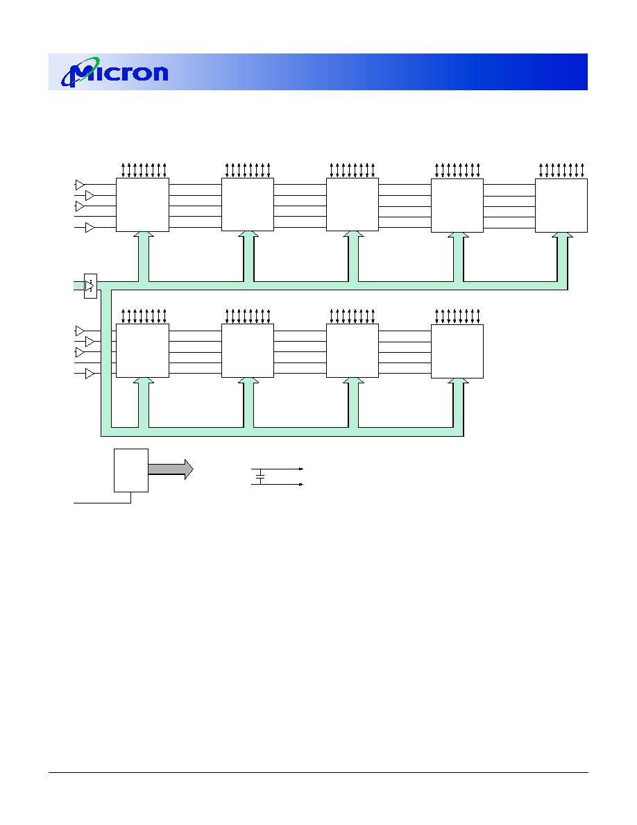
FUNCTIONAL BLOCK DIAGRAM
MT9LD272(X) (16MB)
D
D
D
A10-A1
D
D
D
OE0#
WE0#
CAS0#
RAS0#
D
D
A0
DQ0-DQ7
U9
A1–A10
DQ0-DQ7
DQ0-DQ7
U4
U3
A1–A10
DQ0-DQ7
DQ0-DQ7
U2
U7
A1–A10
A1–A10
DQ0-DQ7
U8
A1–A10
A10
D
A1
A1–A10
DQ0-DQ7
U1
A1–A10
A0
WE#
OE#
RAS#
CAS#
A0
WE#
OE#
RAS#
CAS#
A0
WE#
OE#
RAS#
CAS#
A0
WE#
OE#
RAS#
CAS#
A0
WE#
OE#
RAS#
CAS#
A0
WE#
OE#
RAS#
CAS#
A0
WE#
OE#
RAS#
CAS#
DQ0-DQ7
U5
A1–A10
DQ0-DQ7
DQ64-DQ71
DQ16-DQ23
DQ24-DQ31
DQ8-DQ15
DQ48-DQ55
DQ56-DQ63
DQ0-DQ7
DQ32-DQ39
DQ40-DQ47
U6
A1–A10
U1-U9 = MT4LC2M8B1 FAST PAGE MODE
U1-U9 = MT4LC2M8E7 EDO PAGE MODE
PDE#
PD1-PD8
E#
PRESENCE
DETECT
GENERATOR
OE2#
WE2#
CAS4#
RAS2#
B0
10
10
10
10
10
10
10
10
10
10
V
DD
V
SS
U1-U9, Buffers
U1-U9, Buffers
A0
WE#
OE#
RAS#
CAS#
A0
WE#
OE#
RAS#
CAS#
NOTE: 1. All inputs, with the exception of RAS#, are redriven.
2. D = line buffers.

2, 4 Meg x 72 Buffered DRAM DIMMs
Micron Technology, Inc., reserves the right to change products or specifications without notice.
DM33.p65 ≠ Rev. 2/99
©1999, Micron Technology, Inc.
4
2, 4 MEG x 72
BUFFERED DRAM DIMMs
OBSOLETE
NOTE: 1. All inputs with the exception of RAS# are redriven.
2. D = line buffers.
FUNCTIONAL BLOCK DIAGRAM
MT18LD472(F)(X) (32MB)
DQ0-DQ3
DQ4-DQ7
DQ8-DQ11
DQ12-DQ15
DQ16-DQ19
DQ20-DQ23
DQ24-DQ27
DQ28-DQ31
DQ32-DQ35
DQ36-DQ39
DQ40-DQ43
DQ44-DQ47
DQ48-DQ51
DQ52-DQ55
DQ56-DQ59
DQ60-DQ63
DQ64-DQ67
DQ68-DQ71
MT18LD472FG (4K REFRESH)
U1-U18 = MT4LC4M4A1 FAST PAGE MODE
MT18LD472FG X (4K REFRESH)
U1-U18 = MT4LC4M4E9 EDO PAGE MODE
D
D
D
D
OE0#
D
D
WE0#
CAS0#
OE2#
WE2#
CAS4#
A11-A1
RAS0#
RAS2#
A1–A11
A0
WE#
OE#
RAS#
CAS#
A1–A11
A0
WE#
OE#
RAS#
CAS#
A1–A11
A0
WE#
OE#
RAS#
CAS#
A1–A11
A0
WE#
OE#
RAS#
CAS#
A1–A11
A0
WE#
OE#
RAS#
CAS#
A1–A11
A0
WE#
OE#
RAS#
CAS#
A1–A11
A0
WE#
OE#
RAS#
CAS#
A1–A11
A0
WE#
OE#
RAS#
CAS#
D
A0
D
B0
A11
D
A1
PDE#
PD1-PD8
E#
PRESENCE-
DETECT
GENERATOR
MT18LD472G (2K REFRESH)
U1-U18 = MT4LC4M4B1 FAST PAGE MODE
MT18LD472G X (2K REFRESH)
U1-U18 = MT4LC4M4E8 EDO PAGE MODE
V
DD
V
SS
U1-U18, Buffers
U1-U18, Buffers
A1–A11
A0
WE#
OE#
RAS#
CAS#
A1–A11
A0
WE#
OE#
RAS#
CAS#
A1–A11
A0
WE#
OE#
RAS#
CAS#
A1–A11
A0
WE#
OE#
RAS#
CAS#
A1–A11
A0
WE#
OE#
RAS#
CAS#
A1–A11
A0
WE#
OE#
RAS#
CAS#
A1–A11
A0
WE#
OE#
RAS#
CAS#
A1–A11
A0
WE#
OE#
RAS#
CAS#
A1–A11
A0
WE#
OE#
RAS#
CAS#
A1–A11
A0
WE#
OE#
RAS#
CAS#
DQ0-DQ3
U2
DQ0-DQ3
U3
DQ0-DQ3
U4
U5
DQ0-DQ3
U6
DQ0-DQ3
U7
DQ0-DQ3
DQ0-DQ3
U8
DQ0-DQ3
U9
U16
U17
U15
U18
DQ0-DQ3
DQ0-DQ3
DQ0-DQ3
DQ0-DQ3
U10
U11
U13
U14
U12
DQ0-DQ3
DQ0-DQ3
DQ0-DQ3
DQ0-DQ3
DQ0-DQ3
DQ0-DQ3
U1

2, 4 Meg x 72 Buffered DRAM DIMMs
Micron Technology, Inc., reserves the right to change products or specifications without notice.
DM33.p65 ≠ Rev. 2/99
©1999, Micron Technology, Inc.
5
2, 4 MEG x 72
BUFFERED DRAM DIMMs
OBSOLETE
PIN DESCRIPTIONS
PIN NUMBERS
SYMBOL
TYPE
DESCRIPTION
30, 45
RAS0#, RAS2#
Input
Row-Address Strobe: RAS# is used to clock-in the row-
address bits. Two RAS# inputs allow for one x72 bank
or two x36 banks.
28, 46
CAS0#, CAS4#
Buffered
Column-Address Strobe: CAS# is used to clock-in the
Input
column-address bits, enable the DRAM output buffers
and strobe the data inputs on WRITE cycles.
27, 48
WE0#, WE2#
Buffered
Write Enable: WE# is the READ/WRITE control for the
Input
DQ pins. WE0# controls DQ0-DQ35. WE2# controls
DQ36-DQ71. If WE# is LOW prior to CAS# going LOW,
the access is an EARLY WRITE cycle. If WE# is HIGH
while CAS# is LOW, the access is a READ cycle,
provided OE# is also LOW. If WE# goes LOW after
CAS# goes LOW, then the cycle is a LATE WRITE cycle.
A LATE WRITE cycle is generally used in conjunction
with a READ cycle to form a READ-MODIFY-WRITE
cycle.
31, 44
OE0#, OE2#
Buffered
Output Enable: OE# is the input/output control for the
Input
DQ pins. OE0# controls DQ0-DQ35. OE2# controls
DQ36-DQ71. These signals may be driven, allowing
LATE WRITE cycles.
33-38, 117-122, 126
A0-A11, B0
Buffered
Address Inputs: These inputs are multiplexed and
Input
clocked by RAS# and CAS#. A0 is common to the
DRAMs used for DQ0-DQ35 while B0 is common to the
DRAMs used for DQ36-DQ71
2-5, 7-11, 13-17, 19-22,
DQ0-DQ71
Input/
Data I/O: For WRITE cycles, DQ0-DQ71 act as inputs to
52-53, 55-58, 60, 65-67,
Output
the addressed DRAM location. For READ access cycles,
69-72, 74-77, 86-89,
DQ0-DQ71 act as outputs for the addressed DRAM
91-95, 97-101, 103-106,
location.
136-137, 139-142,
144, 149-151, 153-156,
158-161
79-82, 163-166
PD1-PD8
Buffered
Presence-Detect: These pins are read by the host system
Output
and tell the system the DIMM's personality. They will be
either no connect (1), or they will be driven to V
OL
(0).
29, 41-42, 47, 61-64, 111,
RFU
≠
Reserved for Future Use: These pins should be left
113, 115, 125, 128, 131,
unconnected.
145-148
6, 18, 26, 40, 49, 59, 73,
V
DD
Supply
Power Supply: +3.3V ± 0.3V.
84, 90, 102, 110, 124,
133, 143, 157, 168
1, 12, 23, 32, 43, 54,
V
SS
Supply
Ground.
68, 78, 85, 96, 107, 116,
127, 138, 152, 162
83, 167
ID0, ID1
Output
ID Bits: ID0 = DIMM type. ID1 = Refresh Mode. These
pins will be either left floating (NC) or they will be
grounded (V
SS
).
132
PDE#
Input
Presence-Detect Enable: PDE# is the READ control for
the buffered presence-detect pins.

2, 4 Meg x 72 Buffered DRAM DIMMs
Micron Technology, Inc., reserves the right to change products or specifications without notice.
DM33.p65 ≠ Rev. 2/99
©1999, Micron Technology, Inc.
6
2, 4 MEG x 72
BUFFERED DRAM DIMMs
OBSOLETE
NOTE:
V
SS
= Ground; V
OL
= 0; NC = 1.
* This addressing includes a redundant address to allow mixing of 12/10 and 11/11 DRAMs with the same presence-detect setting.
PRESENCE-DETECT TRUTH TABLE
CHARACTERISTICS
PRESENCE-DETECT PIN (PDx)
Module
Module
Row/Column
ID0
ID1
Density
Configuration
Addresses
1
2
3
4
5
6
7
8
0MB
No module installed
X
1
1
1
1
8MB
1 Meg x 64/72
10/9
1
1
0
0
8MB
1 Meg x 64/72
10/10
0
0
1
0
16MB
2 Meg x 64/72
10/10
1
0
1
0
∑
16MB
2 Meg x 64/72
11/10
1
0
0
1
32MB
4 Meg x 64/72
11/10
0
1
0
1
∑
32MB
4 Meg x 64/72
12*/11*
1
1
0
1
64MB
8 Meg x 64/72
12*/11*
0
0
1
1
Page Mode
Fast Page Mode
0
EDO Page Mode
1
Access Timing
70ns
0
1
60ns
1
1
50ns
0
0
Refresh Control
Standard
Vss
Data Width
x64, No Parity
Vss
1
x72, ECC
Vss
0
2, 4 Meg x 72 Buffered DRAM DIMMs
Micron Technology, Inc., reserves the right to change products or specifications without notice.
DM33.p65 ≠ Rev. 2/99
©1999, Micron Technology, Inc.
7
2, 4 MEG x 72
BUFFERED DRAM DIMMs
OBSOLETE
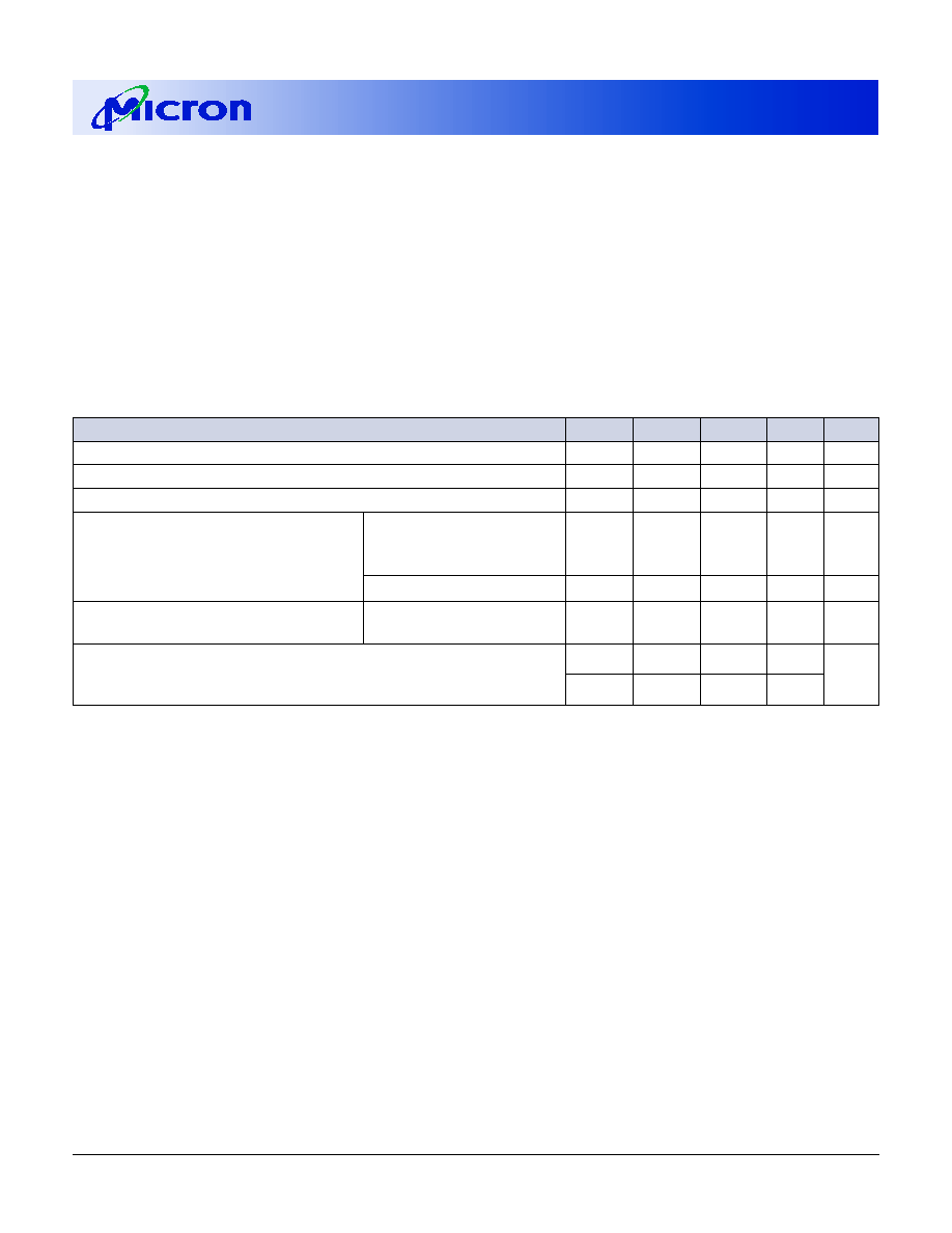
DC ELECTRICAL CHARACTERISTICS AND OPERATING CONDITIONS
(Notes: 1) (V
DD
= +3.3V ±0.3V)
PARAMETER/CONDITION
SYMBOL
MIN
MAX
UNITS NOTES
SUPPLY VOLTAGE
V
DD
3
3.6
V
INPUT HIGH VOLTAGE: Logic 1; All inputs
V
IH
2
V
DD
+ 0.3
V
36
INPUT LOW VOLTAGE: Logic 0; All inputs
V
IL
-0.5
0.8
V
36
INPUT LEAKAGE CURRENT:
CAS0#, CAS4#,
Any input 0V
£ V
IN
£ V
DD
+ 0.3V
A0-A11, B0, PDE#,
I
I
1
-2
2
µA
(All other pins not under test = 0V)
WE0#, WE2#, OE0#, OE2#
RAS0#-RAS3#
I
I
2
-18
18
µA
OUTPUT LEAKAGE CURRENT:
DQ0-DQ71,
I
OZ
-5
5
µA
DQ is disabled; 0V
£ V
OUT
£ V
DD
+ 0.3V
PD1-PD8
OUTPUT LEVELS:
V
OH
2.4
≠
V
Output High Voltage (I
OUT
= -2mA)
Output Low Voltage (I
OUT
= 2mA)
V
OL
≠
0.4
V
ABSOLUTE MAXIMUM RATINGS*
Voltage on V
DD
Pin Relative to V
SS
........ -1V to +4.6V
Voltage on Inputs or I/O Pins
Relative to V
SS
..................................... -1V to +4.6V
Operating Temperature, T
A
(ambient) .. 0∞C to +70∞C
Storage Temperature (plastic) ........... -55∞C to +125∞C
Power Dissipation ................................................... 9W
*Stresses greater than those listed under "Absolute
Maximum Ratings" may cause permanent damage to
the device. This is a stress rating only, and functional
operation of the device at these or any other condi-
tions above those indicated in the operational sections
of this specification is not implied. Exposure to abso-
lute maximum rating conditions for extended periods
may affect reliability.

2, 4 Meg x 72 Buffered DRAM DIMMs
Micron Technology, Inc., reserves the right to change products or specifications without notice.
DM33.p65 ≠ Rev. 2/99
©1999, Micron Technology, Inc.
8
2, 4 MEG x 72
BUFFERED DRAM DIMMs
OBSOLETE
PARAMETER/CONDITION
SYMBOL SIZE
-5*
-6
UNITS NOTES
STANDBY CURRENT: TTL
I
CC
1
16MB
72
72
mA
(RAS# = CAS# = V
IH
)
32MB
90
90
STANDBY CURRENT: CMOS
I
CC
2
16MB
9
9
mA
(RAS# = CAS# = V
DD
- 0.2V)
32MB
9
9
OPERATING CURRENT: Random READ/WRITE
I
CC
3
16MB
990
900
mA
3, 29
Average power supply current
32MB
1,980
1,800
(RAS#, CAS#, address cycling:
t
RC =
t
RC [MIN])
OPERATING CURRENT: FAST PAGE MODE
I
CC
4
16MB
≠
720
mA
3, 29
Average power supply current
32MB
≠
1,440
(RAS# = V
IL
, CAS#, address cycling:
t
PC =
t
PC [MIN])
OPERATING CURRENT: EDO PAGE MODE ("X" version only)
I
CC
5
16MB
990
900
mA
3, 29
Average power supply current
(X only) 32MB
1,980
1,800
(RAS# = V
IL
, CAS#, address cycling:
t
PC =
t
PC [MIN])
REFRESH CURRENT: RAS#-ONLY
I
CC
6
16MB
990
900
mA
3, 29
Average power supply current
32MB
1,980
1,800
(RAS# cycling, CAS# = V
IH
:
t
RC =
t
RC [MIN])
REFRESH CURRENT: CBR
I
CC
7
16MB
990
900
mA
3, 4
Average power supply current
32MB
1,980
1,800
(RAS#, CAS#, address cycling:
t
RC =
t
RC [MIN])
2,048-CYCLE REFRESH I
CC
OPERATING CONDITIONS AND MAXIMUM LIMITS
(Notes: 1, 5, 6) (V
DD
= +3.3V ±0.3V)
MAX
* EDO version only
4,096-CYCLE REFRESH I
CC
OPERATING CONDITIONS AND MAXIMUM LIMITS
(Notes: 1, 5, 6) (V
DD
= +3.3V ±0.3V)
PARAMETER/CONDITION
SYMBOL SIZE
-5*
-6
UNITS NOTES
STANDBY CURRENT: TTL
I
CC
1
32MB
90
90
mA
(RAS# = CAS# = V
IH
)
STANDBY CURRENT: CMOS
I
CC
2
32MB
9
9
mA
(RAS# = CAS# = V
DD
- 0.2V)
OPERATING CURRENT: Random READ/WRITE
Average power supply current
I
CC
3
32MB
1,620
1,440
mA
3, 29
(RAS#, CAS#, address cycling:
t
RC =
t
RC [MIN])
OPERATING CURRENT: FAST PAGE MODE
Average power supply current
I
CC
4
32MB
≠
1,260
mA
3, 29
(RAS# = V
IL
, CAS#, address cycling:
t
PC =
t
PC [MIN])
OPERATING CURRENT: EDO PAGE MODE ("X" version only)
I
CC
5
Average power supply current
(X only) 32MB
1,800
1,620
mA
3, 29
(RAS# = V
IL
, CAS#, address cycling:
t
PC =
t
PC [MIN])
REFRESH CURRENT: RAS#-ONLY
Average power supply current
I
CC
6
32MB
1,620
1,440
mA
3, 29
(RAS# cycling, CAS# = V
IH
:
t
RC =
t
RC [MIN])
REFRESH CURRENT: CBR
Average power supply current
I
CC
7
32MB
1,620
1,440
mA
3, 4
(RAS#, CAS#, address cycling:
t
RC =
t
RC [MIN])
MAX

2, 4 Meg x 72 Buffered DRAM DIMMs
Micron Technology, Inc., reserves the right to change products or specifications without notice.
DM33.p65 ≠ Rev. 2/99
©1999, Micron Technology, Inc.
9
2, 4 MEG x 72
BUFFERED DRAM DIMMs
OBSOLETE
FAST PAGE MODE
AC ELECTRICAL CHARACTERISTICS
(Notes: 5, 6, 7, 8, 9, 12, 35) (V
DD
= +3.3V ±0.3V)
AC CHARACTERISTICS - FAST PAGE MODE OPTION
-6
PARAMETER
SYMBOL
MIN
MAX
UNITS
NOTES
Access time from column address
t
AA
35
ns
23
Column-address hold time (referenced to RAS#)
t
AR
43
ns
22
Column-address setup time
t
ASC
2
ns
21
Row-address setup time
t
ASR
5
ns
23
Column address to WE# delay time
t
AWD
57
ns
21, 28
Access time from CAS#
t
CAC
20
ns
14, 23
Column-address hold time
t
CAH
15
ns
23
CAS# pulse width
t
CAS
15
10,000
ns
CAS# hold time (CBR Refresh)
t
CHR
8
ns
4, 22
CAS# to output in Low-Z
t
CLZ
5
ns
21, 30
CAS# precharge time
t
CP
10
ns
15
Access time from CAS# precharge
t
CPA
40
ns
23
CAS# to RAS# precharge time
t
CRP
10
ns
23
CAS# hold time
t
CSH
58
ns
22
CAS# setup time (CBR Refresh)
t
CSR
7
ns
4, 21
CAS# to WE# delay time
t
CWD
42
ns
21, 28
WRITE command to CAS# lead time
t
CWL
15
ns
Data-in hold time
t
DH
15
ns
23, 27
Data-in setup time
t
DS
-2
ns
22, 27
Output disable
t
OD
3
15
ns
Output enable
t
OE
15
ns
OE# hold time from WE# during READ-MODIFY-WRITE cycle
t
OEH
13
ns
22, 26
Output buffer turn-off delay
t
OFF
5
20
ns
19, 25, 33
OE# setup prior to RAS# during HIDDEN REFRESH cycle
t
ORD
0
ns
FAST-PAGE-MODE READ or WRITE cycle time
t
PC
35
ns
CAPACITANCE
PARAMETER
SYMBOL 16MB 32MB UNITS NOTES
Input Capacitance: A0-A11, B0, PDE#, OE0#, OE2#
C
I
1
9
9
p F
2
Input Capacitance: WE0#, WE2#, CAS0#, CAS4#
C
I
2
9
9
p F
2
Input Capacitance: RAS0#, RAS2#
C
I
3
39
67
p F
2
Input/Output Capacitance: DQ0-DQ71
C
IO
10
10
p F
2
Output Capacitance: PD1-PD8
C
O
10
10
p F
2
MAX
2, 4 Meg x 72 Buffered DRAM DIMMs
Micron Technology, Inc., reserves the right to change products or specifications without notice.
DM33.p65 ≠ Rev. 2/99
©1999, Micron Technology, Inc.
10
2, 4 MEG x 72
BUFFERED DRAM DIMMs
OBSOLETE
FAST PAGE MODE
AC ELECTRICAL CHARACTERISTICS
(Notes: 5, 6, 7, 8, 9, 12, 35) (V
DD
= +3.3V ±0.3V)
AC CHARACTERISTICS - FAST PAGE MODE OPTION
-6
PARAMETER
SYMBOL
MIN
MAX
UNITS
NOTES
PDE# to valid presence-detect data
t
PD
10
ns
32
PDE# inactive to presence-detects inactive
t
PDOFF
2
ns
31
FAST-PAGE-MODE READ-WRITE cycle time
t
PRWC
87
ns
21
Access time from RAS#
t
RAC
60
ns
13
RAS# to column-address delay time
t
RAD
13
ns
17, 24
Row-address hold time
t
RAH
8
ns
22
RAS# pulse width
t
RAS
60
10,000
ns
RAS# pulse width (FAST PAGE MODE)
t
RASP
60
125,000
ns
Random READ or WRITE cycle time
t
RC
110
ns
RAS# to CAS# delay time
t
RCD
18
ns
16, 24
READ command hold time (referenced to CAS#)
t
RCH
2
ns
18, 21
READ command setup time
t
RCS
2
ns
21
Refresh period (2,048 cycles) (16MB)
t
REF
32
ms
Refresh period (4,096 cycles) (32MB)
t
REF
64
ms
RAS# precharge time
t
RP
40
ns
RAS# to CAS# precharge time
t
RPC
0
ns
READ command hold time (referenced to RAS#)
t
RRH
0
ns
18
RAS# hold time
t
RSH
20
ns
23
READ-WRITE cycle time
t
RWC
160
ns
23
RAS# to WE# delay time
t
RWD
87
ns
21, 28
WRITE command to RAS# lead time
t
RWL
20
ns
23
Transition time (rise or fall)
t
T
2
50
ns
WRITE command hold time
t
WCH
15
ns
23
WRITE command hold time (referenced to RAS#)
t
WCR
43
ns
22
WE# command setup time
t
WCS
2
ns
21, 28
WRITE command pulse width
t
WP
10
ns
WE# hold time (CBR Refresh)
t
WRH
8
ns
22
WE# setup time (CBR Refresh)
t
WRP
12
ns
21
2, 4 Meg x 72 Buffered DRAM DIMMs
Micron Technology, Inc., reserves the right to change products or specifications without notice.
DM33.p65 ≠ Rev. 2/99
©1999, Micron Technology, Inc.
11
2, 4 MEG x 72
BUFFERED DRAM DIMMs
OBSOLETE
EDO PAGE MODE
AC ELECTRICAL CHARACTERISTICS
(Notes: 5, 6, 7, 8, 9, 12, 35) (V
DD
= +3.3V ±0.3V)
AC CHARACTERISTICS - EDO PAGE MODE OPTION
-5
-6
PARAMETER
SYMBOL
MIN
MAX
MIN
MAX
UNITS
NOTES
Access time from column address
t
AA
30
35
ns
23
Column-address setup to CAS# precharge
t
ACH
12
15
ns
Column-address hold time (referenced to RAS#)
t
AR
36
43
ns
22
Column-address setup time
t
ASC
2
2
ns
21
Row-address setup time
t
ASR
5
5
ns
23
Column address to WE# delay time
t
AWD
44
51
ns
21, 28
Access time from CAS#
t
CAC
18
20
ns
14, 23
Column-address hold time
t
CAH
13
15
ns
23
CAS# pulse width
t
CAS
8
10,000
10
10,000
ns
CAS# hold time (CBR Refresh)
t
CHR
6
8
ns
4, 22
CAS# to output in Low-Z
t
CLZ
2
2
ns
21
Data output hold after next CAS# LOW
t
COH
5
5
ns
21
CAS# precharge time
t
CP
8
10
ns
15
Access time from CAS# precharge
t
CPA
33
40
ns
23
CAS# to RAS# precharge time
t
CRP
10
10
ns
23
CAS# hold time
t
CSH
36
43
ns
22
CAS# setup time (CBR Refresh)
t
CSR
7
7
ns
4, 21
CAS# to WE# delay time
t
CWD
30
37
ns
21, 28
WRITE command to CAS# lead time
t
CWL
8
10
ns
Data-in hold time
t
DH
13
15
ns
23, 27
Data-in setup time
t
DS
-2
-2
ns
22, 27
Output disable
t
OD
0
12
0
15
ns
Output enable
t
OE
12
15
ns
OE# hold time from WE# during
t
OEH
6
8
ns
22, 26
READ-MODIFY-WRITE cycle
OE# HIGH hold from CAS# HIGH
t
OEHC
5
10
ns
26
OE# HIGH pulse width
t
OEP
5
5
ns
OE# LOW to CAS# HIGH setup time
t
OES
4
5
ns
Output buffer turn-off delay
t
OFF
2
17
2
20
ns
19, 25, 33

2, 4 Meg x 72 Buffered DRAM DIMMs
Micron Technology, Inc., reserves the right to change products or specifications without notice.
DM33.p65 ≠ Rev. 2/99
©1999, Micron Technology, Inc.
12
2, 4 MEG x 72
BUFFERED DRAM DIMMs
OBSOLETE
EDO PAGE MODE
AC ELECTRICAL CHARACTERISTICS
(Notes: 5, 6, 7, 8, 9, 12, 35) (V
DD
= +3.3V ±0.3V)
AC CHARACTERISTICS - EDO PAGE MODE OPTION
-5
-6
PARAMETER
SYMBOL
MIN
MAX
MIN
MAX
UNITS
NOTES
OE# setup prior to RAS#
t
ORD
0
0
ns
during HIDDEN REFRESH cycle
EDO-PAGE-MODE READ or WRITE cycle time
t
PC
20
25
ns
PDE# to valid presence-detect data
t
PD
10
10
ns
32
PDE# inactive to presence-detect inactive
t
PDOFF
2
2
ns
31
EDO-PAGE-MODE READ-WRITE cycle time
t
PRWC
49
58
ns
21
Access time from RAS#
t
RAC
50
60
ns
13
RAS# to column-address delay time
t
RAD
7
10
ns
17, 22
Row-address hold time
t
RAH
7
8
ns
22
RAS# pulse width
t
RAS
50
10,000
60
10,000
ns
RAS# pulse width (EDO PAGE MODE)
t
RASP
50
125,000
60
125,000
ns
Random READ or WRITE cycle time
t
RC
84
104
ns
RAS# to CAS# delay time
t
RCD
9
12
ns
16, 24
READ command hold time (referenced to CAS#)
t
RCH
2
2
ns
18, 21
READ command setup time
t
RCS
2
2
ns
21
Refresh period (2,048 cycles) (16MB)
t
REF
32
32
ms
Refresh period (4,096 cycles) (32MB)
t
REF
64
64
ms
RAS# precharge time
t
RP
30
40
ns
RAS# to CAS# precharge time
t
RPC
5
5
ns
READ command hold time (referenced to RAS#)
t
RRH
0
0
ns
18
RAS# hold time
t
RSH
18
20
ns
23
READ-ZWRITE cycle time
t
RWC
121
145
ns
23
RAS# to WE# delay time
t
RWD
69
81
ns
21, 28
WRITE command to RAS# lead time
t
RWL
18
20
ns
23
Transition time (rise or fall)
t
T
2
50
2
50
ns
WRITE command hold time
t
WCH
13
15
ns
23
WRITE command hold time (referenced to RAS#)
t
WCR
36
43
ns
22
WE# command setup time
t
WCS
2
2
ns
21, 28
Output disable delay from WE#
t
WHZ
2
17
2
20
ns
25
WRITE command pulse width
t
WP
5
5
ns
WE# pulse to disable at CAS# HIGH
t
WPZ
10
10
ns
WE# hold time (CBR Refresh)
t
WRH
6
8
ns
22
WE# setup time (CBR Refresh)
t
WRP
10
12
ns
21

2, 4 Meg x 72 Buffered DRAM DIMMs
Micron Technology, Inc., reserves the right to change products or specifications without notice.
DM33.p65 ≠ Rev. 2/99
©1999, Micron Technology, Inc.
13
2, 4 MEG x 72
BUFFERED DRAM DIMMs
OBSOLETE
NOTES
1. All voltages referenced to V
SS
.
2. This parameter is sampled. V
DD
= +3.3V; f = 1 MHz.
3. I
CC
is dependent on output loading. Specified
values are obtained with minimum cycle time and
the outputs open.
4. Enables on-chip refresh and address counters.
5. The minimum specifications are used only to
indicate cycle time at which proper operation over
the full temperature range is ensured.
6. An initial pause of 100µs is required after power-
up, followed by eight RAS# REFRESH cycles
(RAS#-ONLY or CBR with WE# HIGH), before
proper device operation is ensured. The eight RAS#
cycle wake-ups should be repeated any time the
t
REF refresh requirement is exceeded.
7. AC characteristics assume
t
T = 5ns for FPM and
2.5ns for EDO.
8. V
IH
(MIN) and V
IL
(MAX) are reference levels for
measuring timing of input signals. Transition times
are measured between V
IH
and V
IL
(or between V
IL
and V
IH
).
9. In addition to meeting the transition rate
specification, all input signals must transit between
V
IH
and V
IL
(or between V
IL
and V
IH
) in a mono-
tonic manner.
10.If CAS# = V
IH
, data output is High-Z.
11.If CAS# = V
IL
, data output may contain data from
the last valid READ cycle.
12.Measured with a load equivalent to two TTL gates
and 100pF and V
OL
= 0.8V and V
OH
= 2V.
13.Requires that
t
AA and
t
CAC are not violated.
14.Requires that
t
AA and
t
RAC are not violated.
15.If CAS# is LOW at the falling edge of RAS#, Q will
be maintained from the previous cycle. To initiate
a new cycle and clear the data-out buffer, CAS#
must be pulsed HIGH for
t
CP.
16.The
t
RCD (MAX) limit is no longer specified.
t
RCD
(MAX) was specified as a reference point only. If
t
RCD was greater than the specified
t
RCD (MAX)
limit, then access time was controlled exclusively
by
t
CAC (
t
RAC [MIN] no longer applied). With or
without the
t
RCD (MAX) limit,
t
AA and
t
CAC
must always be met.
17.The
t
RAD (MAX) limit is no longer specified.
t
RAD
(MAX) was specified as a reference point only. If
t
RAD was greater than the specified
t
RAD (MAX)
limit, then access time was controlled exclusively
by
t
AA (
t
RAC and
t
CAC no longer applied). With
or without the
t
RAD (MAX) limit,
t
AA,
t
RAC and
t
CAC must always be met.
18.Either
t
RCH or
t
RRH must be satisfied for a READ
cycle.
19.
t
OFF (MAX) defines the time at which the output
achieves the open circuit condition and is not
referenced to V
OH
or V
OL
.
20.A HIDDEN REFRESH may also be performed after
a WRITE cycle. In this case, WE# = LOW and OE#
= HIGH.
21.A +2ns timing skew from the DRAM to the
module resulted from the addition of line drivers.
22.A -2ns timing skew from the DRAM to the module
resulted from the addition of line drivers.
23.A +5ns timing skew from the DRAM to the
module resulted from the addition of line drivers.
24.A -2ns (MIN) and a -5ns (MAX) timing skew from
the DRAM to the module resulted from the
addition of line drivers.
25.A +2ns (MIN) and a +5ns (MAX) timing skew from
the DRAM to the module resulted from the
addition of line drivers.
26.LATE WRITE and READ-MODIFY-WRITE cycles
must have both
t
OD and
t
OEH met (OE# HIGH
during WRITE cycle) in order to ensure that the
output buffers will be open during the WRITE
cycle. The DQs will provide the previously read
data if CAS# remains LOW and OE# is taken back
LOW after
t
OEH is met. If CAS# goes HIGH prior
to OE# going back LOW, the DQs will remain
open.
27.These parameters are referenced to CAS# leading
edge in EARLY WRITE cycles and WE# leading
edge in LATE WRITE or READ-MODIFY-WRITE
cycles.
28.
t
WCS,
t
RWD,
t
AWD and
t
CWD are not restrictive
operating parameters.
t
WCS applies to EARLY
WRITE cycles.
t
RWD,
t
AWD and
t
CWD apply to
READ-MODIFY-WRITE cycles. If
t
WCS
≥
t
WCS
(MIN), the cycle is an EARLY WRITE cycle and the
data output will remain an open circuit through-
out the entire cycle. If
t
WCS <
t
WCS (MIN) and
t
RWD
≥
t
RWD (MIN),
t
AWD
≥
t
AWD (MIN) and
t
CWD
≥
t
CWD (MIN), the cycle is a READ-
MODIFY-WRITE and the data output will contain
data read from the selected cell. If neither of the
above conditions is met, the state of data-out is
indeterminate. OE# held HIGH and WE# taken
LOW after CAS# goes LOW result in a LATE
WRITE (OE#-controlled) cycle.
t
WCS,
t
RWD,
t
CWD and
t
AWD are not applicable in a LATE
WRITE cycle.
29.Column address changed once each cycle.
30.The 3ns minimum parameter guaranteed by
design.

2, 4 Meg x 72 Buffered DRAM DIMMs
Micron Technology, Inc., reserves the right to change products or specifications without notice.
DM33.p65 ≠ Rev. 2/99
©1999, Micron Technology, Inc.
14
2, 4 MEG x 72
BUFFERED DRAM DIMMs
OBSOLETE
NOTES (continued)
31.
t
PDOFF MAX is determined by the pull-up resistor
value. Care must be taken to ensure adequate
recovery time prior to reading valid up-level on
subsequent DIMM position.
32.Measured with specified current load and 100pF.
33.With the FPM option,
t
OFF is determined by the
first RAS# or CAS# signal to transition HIGH. In
comparison,
t
OFF on an EDO option is deter-
mined by the latter of the RAS# and CAS# signals
to transition HIGH.
34.Applies to both FPM and EDO operating modes.
35.If OE# is tied permanently LOW, LATE WRITE or
READ-MODIFY-WRITE operations are not
possible.
36. V
IH
overshoot: V
IH
(MAX) = V
DD
+ 2V for a pulse
width
£ 10ns, and the pulse width cannot be
greater than one third of the cycle rate. V
IL
undershoot: V
IL
(MIN) = -2V for a pulse width
£
10ns, and the pulse width cannot be greater than
one third of the cycle rate.

2, 4 Meg x 72 Buffered DRAM DIMMs
Micron Technology, Inc., reserves the right to change products or specifications without notice.
DM33.p65 ≠ Rev. 2/99
©1999, Micron Technology, Inc.
15
2, 4 MEG x 72
BUFFERED DRAM DIMMs
OBSOLETE
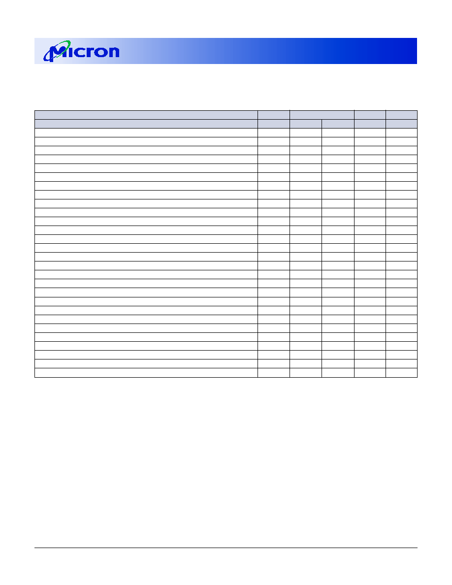
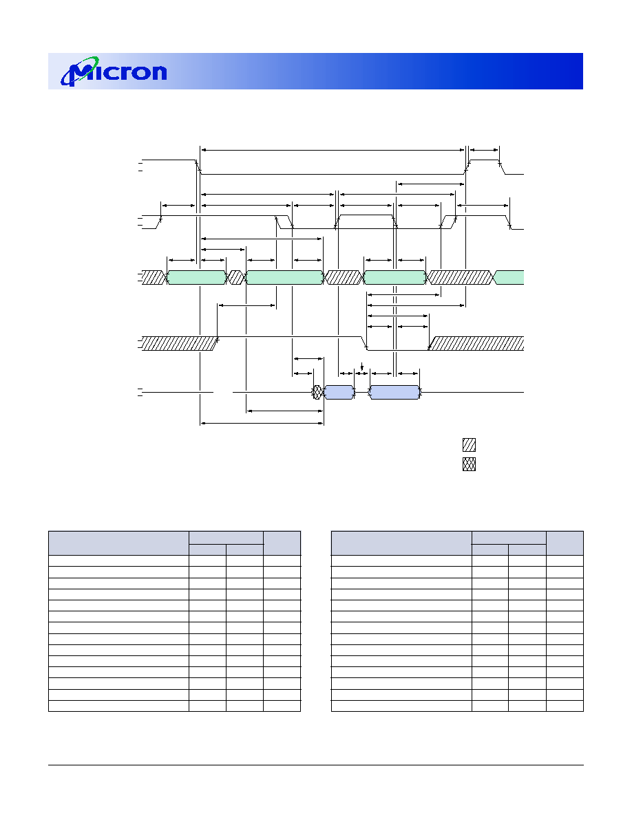
READ CYCLE
34
NOTE: 1. For EDO,
t
OFF is referenced from rising edge of RAS# or CAS#, whichever occurs last. For FPM,
t
OFF is referenced from
rising edge of RAS# or CAS#, whichever occurs first.
tRRH
tCLZ
tCAC
tRAC
tAA
VALID DATA
OPEN
tOFF
tRCH
ROW
tRCS
tASC
tRAH
tRAD
tAR
tCAH
tRCD
tCAS
tRSH
tCSH
tRP
tRC
tRAS
tCRP
tASR
ROW
OPEN
RAS#
V
V
IH
IL
V
V
IH
IL
ADDR
V
V
IH
IL
DQ
V
V
OH
OL
V
V
IH
IL
tOD
tOE
OE#
V
V
IH
IL
COLUMN
CAS#
WE#
NOTE 1
DON'T CARE
UNDEFINED
-5*
-6
SYMBOL
MIN
MAX
MIN
MAX
UNITS
t
OFF (EDO)
2
17
2
20
ns
t
OFF (FPM)
≠
≠
5
20
ns
t
RAC
50
60
ns
t
RAD (EDO)
7
10
ns
t
RAD (FPM)
≠
13
ns
t
RAH
7
8
ns
t
RAS
50
10,000
60
10,000
ns
t
RC (EDO)
84
104
ns
t
RC (FPM)
≠
110
ns
t
RCD (EDO)
9
12
ns
t
RCD (FPM)
≠
18
ns
t
RCH
2
2
ns
t
RCS
2
2
ns
t
RP
30
40
ns
t
RRH
0
0
ns
t
RSH
18
20
ns
FAST PAGE MODE AND EDO PAGE MODE
TIMING PARAMETERS
-5*
-6
SYMBOL
MIN
MAX
MIN
MAX
UNITS
t
AA
30
35
ns
t
ACH (EDO)
12
15
ns
t
AR
36
43
ns
t
ASC
2
2
ns
t
ASR
5
5
ns
t
CAC
18
20
ns
t
CAH
13
15
ns
t
CAS (EDO)
8
10,000
10
10,000
ns
t
CAS (FPM)
≠
≠
15
10,000
ns
t
CLZ (EDO)
2
2
ns
t
CLZ (FPM)
≠
5
ns
t
CRP
10
10
ns
t
CSH (EDO)
36
43
ns
t
CSH (FPM)
≠
58
ns
t
OD (EDO)
0
12
0
15
ns
t
OD (FPM)
≠
≠
3
15
ns
t
OE
12
15
ns
*EDO version only

2, 4 Meg x 72 Buffered DRAM DIMMs
Micron Technology, Inc., reserves the right to change products or specifications without notice.
DM33.p65 ≠ Rev. 2/99
©1999, Micron Technology, Inc.
16
2, 4 MEG x 72
BUFFERED DRAM DIMMs
OBSOLETE
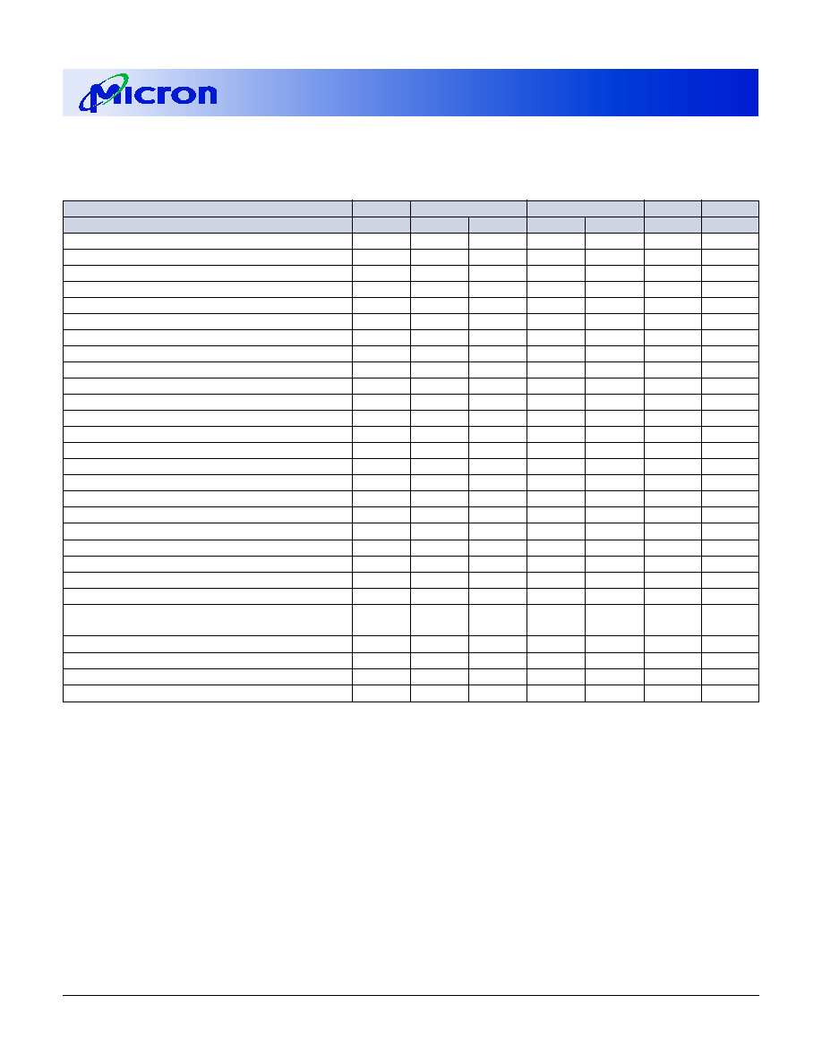
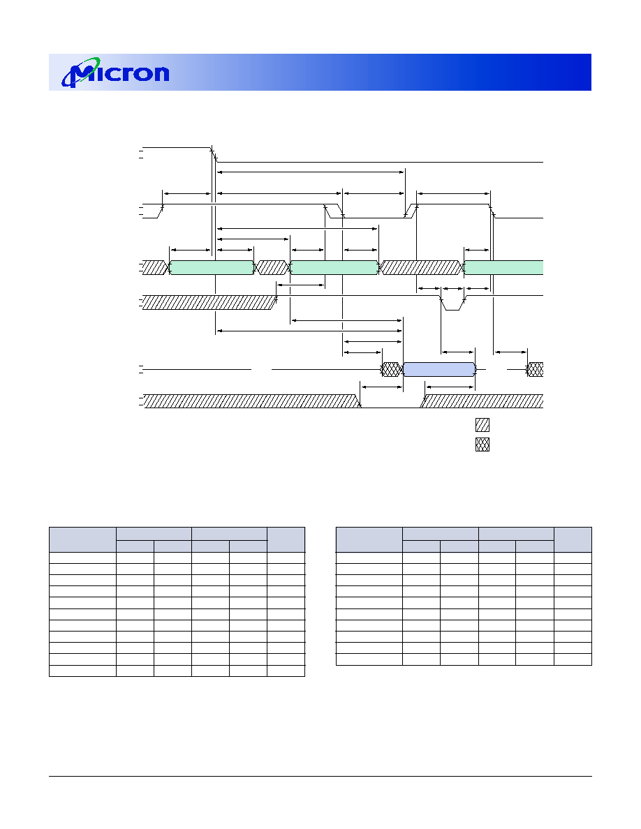
EARLY WRITE CYCLE
34
DON'T CARE
UNDEFINED
V
V
IH
IL
VALID DATA
ROW
COLUMN
ROW
tDS
tWP
tWCH
tWCS
tWCR
tRWL
tCWL
tCAH
tASC
tRAH
tASR
tRAD
tAR
tCAS
tRSH
tCSH
tRCD
tCRP
tRAS
tRC
tRP
V
V
IH
IL
ADDR
V
V
IH
IL
V
V
IH
IL
DQ
V
V
IOH
IOL
V
V
IH
IL
RAS#
OE#
tDH
WE#
CAS#
tACH
*EDO version only
-5*
-6
SYMBOL
MIN
MAX
MIN
MAX
UNITS
t
RAD (EDO)
7
10
ns
t
RAH
7
8
ns
t
RAS
50
10,000
60
10,000
ns
t
RC (FPM)
≠
110
ns
t
RC (EDO)
84
104
ns
t
RCD (FPM)
≠
18
ns
t
RCD (EDO)
9
12
ns
t
RP
30
40
ns
t
RSH
18
20
ns
t
RWL
18
20
ns
t
WCH
13
15
ns
t
WCR
36
43
ns
t
WCS
2
2
ns
t
WP (FPM)
≠
10
ns
t
WP (EDO)
5
5
ns
FAST PAGE MODE AND EDO PAGE MODE
TIMING PARAMETERS
-5*
-6
SYMBOL
MIN
MAX
MIN
MAX
UNITS
t
ACH (EDO)
12
15
ns
t
AR
36
43
ns
t
ASC
2
2
ns
t
ASR
5
5
ns
t
CAH
13
15
ns
t
CAS (FPM)
≠
≠
15
10,000
ns
t
CAS (EDO)
8
10,000
10
10,000
ns
t
CRP
10
10
ns
t
CSH (FPM)
≠
58
ns
t
CSH (EDO)
36
43
ns
t
CWL (FPM)
≠
15
ns
t
CWL (EDO)
8
10
ns
t
DH
13
15
ns
t
DS
-2
-2
ns
t
RAD (FPM)
≠
13
ns

2, 4 Meg x 72 Buffered DRAM DIMMs
Micron Technology, Inc., reserves the right to change products or specifications without notice.
DM33.p65 ≠ Rev. 2/99
©1999, Micron Technology, Inc.
17
2, 4 MEG x 72
BUFFERED DRAM DIMMs
OBSOLETE
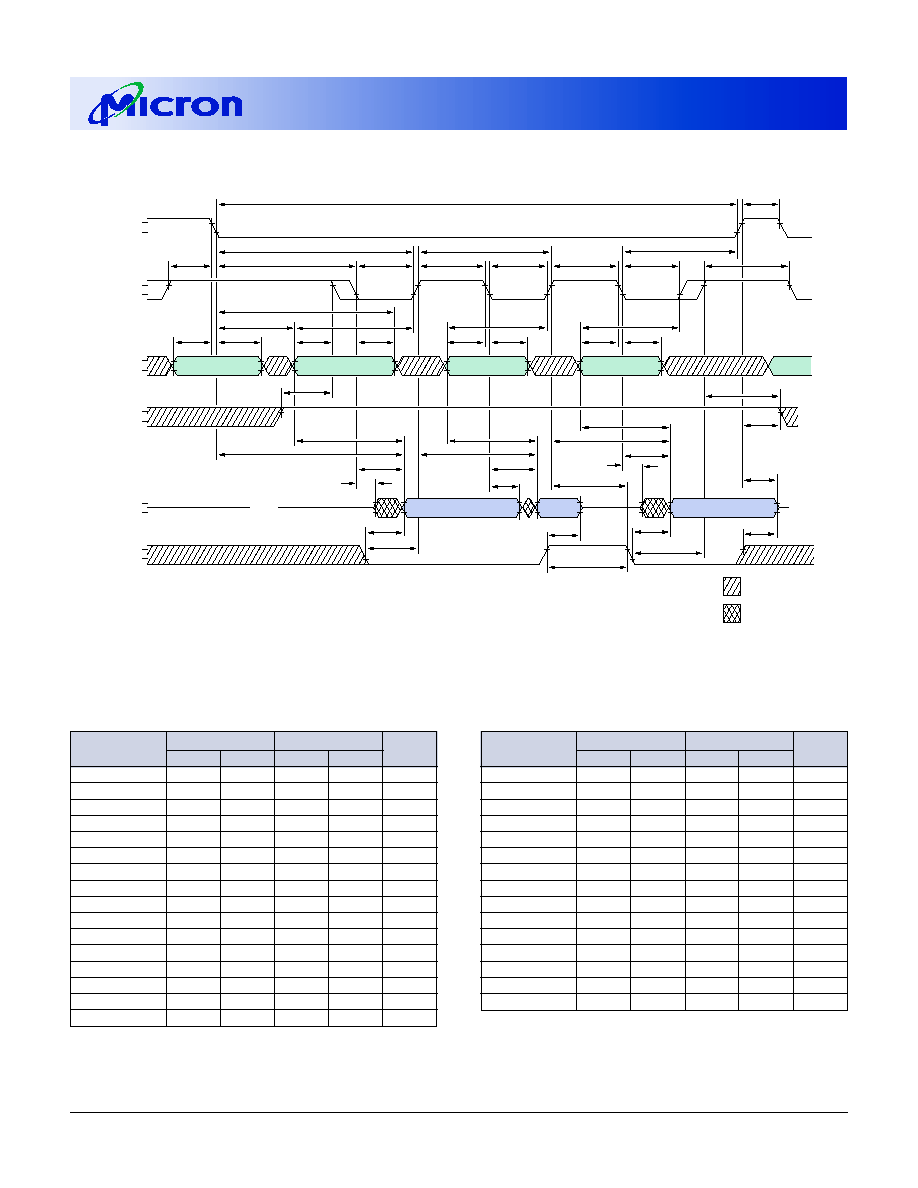
FAST-PAGE-MODE READ CYCLE
tRRH
tCLZ
tCAC
tRAC
tAA
VALID DATA
OPEN
tOFF
tRCH
ROW
tRCS
tASC
tRAH
tRAD
tAR
tCAH
tRAL
tRCD
tCAS
tRSH
tCSH
tRP
tRC
tRAS
tCRP
tASR
ROW
OPEN
RAS
V
V
IH
IL
CAS
V
V
IH
IL
ADDR
V
V
IH
IL
DQ
V
V
IOH
IOL
V
V
IH
IL
tOD
tOE
OE
V
V
IH
IL
COLUMN
WE
DON'T CARE
UNDEFINED
-6
SYMBOL
MIN
MAX
UNITS
t
OE
15
ns
t
OFF
5
20
ns
t
PC
35
ns
t
RAC
60
ns
t
RAD
13
ns
t
RAH
8
ns
t
RASP
60
125,000
ns
t
RCD
18
ns
t
RCH
2
ns
t
RCS
2
ns
t
RP
40
ns
t
RRH
0
ns
t
RSH
20
ns
FAST PAGE MODE
TIMING PARAMETERS
-6
SYMBOL
MIN
MAX
UNITS
t
AA
35
ns
t
AR
43
ns
t
ASC
2
ns
t
ASR
5
ns
t
CAC
20
ns
t
CAH
15
ns
t
CAS
15
10,000
ns
t
CLZ
5
ns
t
CP
10
ns
t
CPA
40
ns
t
CRP
10
ns
t
CSH
58
ns
t
OD
3
15
ns
2, 4 Meg x 72 Buffered DRAM DIMMs
Micron Technology, Inc., reserves the right to change products or specifications without notice.
DM33.p65 ≠ Rev. 2/99
©1999, Micron Technology, Inc.
18
2, 4 MEG x 72
BUFFERED DRAM DIMMs
OBSOLETE
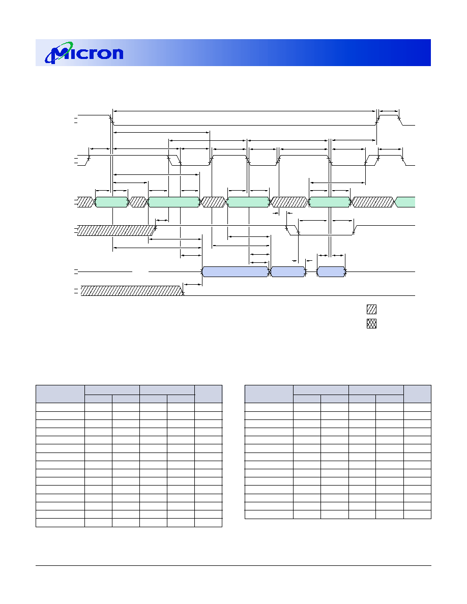
EDO-PAGE-MODE READ CYCLE
VALID
DATA
VALID
DATA
VALID
DATA
COLUMN
COLUMN
COLUMN
ROW
ROW
DON'T CARE
UNDEFINED
tOD
tCAH
tASC
tCP
tRSH
tCP
tCP
tCAS
tRCD
tCRP
tPC
tCSH
tRASP
tRP
tCAH
tASC
tCAH
tASC
tAR
tRAH
tRAD
tASR
tRCS
tRRH
tRCH
tOFF
tCAC
tCPA
tAA
tCLZ
tCAC
tCPA
tAA
tCAC
tRAC
tAA
tCLZ
tOE
tOD
tOE
tOD
OPEN
OPEN
V
V
IH
IL
V
V
IH
IL
ADDR
V
V
IH
IL
V
V
IH
IL
DQ
V
V
OH
OL
V
V
IH
IL
RAS#
OE#
tCAS
tCAS
CAS#
WE#
tCOH
tOEP
tOEHC
tOES
tOES
tACH
tACH
tACH
-5
-6
SYMBOL
MIN
MAX
MIN
MAX
UNITS
t
OEHC
5
10
ns
t
OEP
5
5
ns
t
OES
4
5
ns
t
OFF
2
17
2
20
ns
t
PC
20
25
ns
t
RAC
50
60
ns
t
RAD
7
10
ns
t
RAH
7
8
ns
t
RASP
50
125,000
60
125,000
ns
t
RCD
9
12
ns
t
RCH
2
2
ns
t
RCS
2
2
ns
t
RP
30
40
ns
t
RRH
0
0
ns
t
RSH
18
20
ns
EDO PAGE MODE
TIMING PARAMETERS
-5
-6
SYMBOL
MIN
MAX
MIN
MAX
UNITS
t
AA
30
35
ns
t
ACH
12
15
ns
t
AR
36
43
ns
t
ASC
2
2
ns
t
ASR
5
5
ns
t
CAC
18
20
ns
t
CAH
13
15
ns
t
CAS
8
10,000
10
10,000
ns
t
CLZ
2
2
ns
t
COH
5
5
ns
t
CP
8
10
ns
t
CPA
33
40
ns
t
CRP
10
10
ns
t
CSH
36
43
ns
t
OD
0
12
0
15
ns
t
OE
12
15
ns

2, 4 Meg x 72 Buffered DRAM DIMMs
Micron Technology, Inc., reserves the right to change products or specifications without notice.
DM33.p65 ≠ Rev. 2/99
©1999, Micron Technology, Inc.
19
2, 4 MEG x 72
BUFFERED DRAM DIMMs
OBSOLETE
FAST/EDO-PAGE-MODE EARLY WRITE CYCLE
34
*EDO version only
tDS
tDH
tDS
tDH
tDS
tDH
tWCR
VALID DATA
VALID DATA
VALID DATA
tRWL
tWP
tCWL
tWCH
tWCS
tWP
tCWL
tWCH
tWCS
tWP
tCWL
tWCH
tWCS
tCAH
tASC
tCAH
tASC
tCAH
tASC
tRAH
tASR
tRAD
tACH
tACH
tACH
tAR
COLUMN
COLUMN
COLUMN
ROW
ROW
tCP
tCAS
tRSH
tCP
tCAS
tCP
tCAS
tRCD
tCRP
tPC
tCSH
tRASP
t RP
V
V
IH
IL
CAS#
V
V
IH
IL
ADDR
V
V
IH
IL
WE#
V
V
IH
IL
DQ
V
V
IOH
IOL
RAS#
DON'T CARE
UNDEFINED
-5*
-6
SYMBOL
MIN
MAX
MIN
MAX
UNITS
t
PC (FPM)
≠
35
ns
t
RAD (EDO)
7
10
ns
t
RAD (FPM)
≠
13
ns
t
RAH
7
8
ns
t
RASP
50
125,000
60
125,000
ns
t
RCD (EDO)
9
12
ns
t
RCD (FPM)
≠
18
ns
t
RP
30
40
ns
t
RSH
18
20
ns
t
RWL
18
20
ns
t
WCH
13
15
ns
t
WCR
36
43
ns
t
WCS
2
2
ns
t
WP (EDO)
5
5
ns
t
WP (FPM)
≠
10
ns
FAST PAGE MODE AND EDO PAGE MODE
TIMING PARAMETERS
-5*
-6
SYMBOL
MIN
MAX
MIN
MAX
UNITS
t
ACH (EDO)
12
15
ns
t
AR
36
43
ns
t
ASC
2
2
ns
t
ASR
5
5
ns
t
CAH
13
15
ns
t
CAS (EDO)
8
10,000
10
10,000
ns
t
CAS (FPM)
≠
≠
15
10,000
ns
t
CP
8
10
ns
t
CRP
10
10
ns
t
CSH (EDO)
36
43
ns
t
CSH (FPM)
≠
58
ns
t
CWL (EDO)
8
10
ns
t
CWL (FPM)
≠
15
ns
t
DH
13
15
ns
t
DS
-2
-2
ns
t
PC (EDO)
20
25
ns

2, 4 Meg x 72 Buffered DRAM DIMMs
Micron Technology, Inc., reserves the right to change products or specifications without notice.
DM33.p65 ≠ Rev. 2/99
©1999, Micron Technology, Inc.
20
2, 4 MEG x 72
BUFFERED DRAM DIMMs
OBSOLETE
READ-WRITE CYCLE
34
(LATE WRITE and READ-MODIFY-WRITE cycles)
VALID D
OUT
VALID D
IN
ROW
COLUMN
ROW
V
V
IH
IL
V
V
IH
IL
ADDR
V
V
IH
IL
V
V
IH
IL
DQ
V
V
IOH
IOL
V
V
IH
IL
RAS#
OPEN
OPEN
tOE
tOD
tCAC
tRAC
tAA
t CLZ
tDS
tDH
tAWD
tWP
tRWL
tCWL
tCWD
tRWD
tRCS
tASC
tCAH
tAR
tASR
tRAD
tCRP
tRCD
tCAS
tRSH
tCSH
tRAS
tRWC
tRP
tRAH
OE#
tOEH
WE#
tACH
CAS#
DON'T CARE
UNDEFINED
*EDO version only
-5*
-6
SYMBOL
MIN
MAX
MIN
MAX
UNITS
t
OD (EDO)
0
12
0
15
ns
t
OD (FPM)
≠
≠
3
15
ns
t
OE
12
15
ns
t
OEH (EDO)
6
8
ns
t
OEH (FPM)
≠
13
ns
t
RAC
50
60
ns
t
RAD (EDO)
7
10
ns
t
RAD (FPM)
≠
13
ns
t
RAH
7
8
ns
t
RAS
50
10,000
60
10,000
ns
t
RCD (EDO)
9
12
ns
t
RCD (FPM)
≠
18
ns
t
RCS
2
2
ns
t
RP
30
40
ns
t
RSH
18
20
ns
t
RWC (EDO)
121
145
ns
t
RWC (FPM)
≠
160
ns
t
RWD (EDO)
69
81
ns
t
RWD (FPM)
≠
87
ns
t
RWL
18
20
ns
t
WP (EDO)
5
5
ns
t
WP (FPM)
≠
10
ns
FAST PAGE MODE AND EDO PAGE MODE
TIMING PARAMETERS
-5*
-6
SYMBOL
MIN
MAX
MIN
MAX
UNITS
t
AA
30
35
ns
t
ACH (EDO)
12
15
ns
t
AR
36
43
ns
t
ASC
2
2
ns
t
ASR
5
5
ns
t
AWD (EDO)
42
49
ns
t
AWD (FPM)
≠
57
ns
t
CAC
18
20
ns
t
CAH
13
15
ns
t
CAS (EDO)
8
10,000
10
10,000
ns
t
CAS (FPM)
≠
≠
15
10,000
ns
t
CLZ (EDO)
2
2
ns
t
CLZ (FPM)
≠
5
ns
t
CRP
10
10
ns
t
CSH (EDO)
36
43
ns
t
CSH (FPM)
≠
58
ns
t
CWD (EDO)
30
37
ns
t
CWD (FPM)
≠
42
ns
t
CWL (EDO)
8
10
ns
t
CWL (FPM)
≠
15
ns
t
DH
13
15
ns
t
DS
-2
-2
ns

2, 4 Meg x 72 Buffered DRAM DIMMs
Micron Technology, Inc., reserves the right to change products or specifications without notice.
DM33.p65 ≠ Rev. 2/99
©1999, Micron Technology, Inc.
21
2, 4 MEG x 72
BUFFERED DRAM DIMMs
OBSOLETE
FAST/EDO-PAGE-MODE READ-WRITE CYCLE
34
(LATE WRITE and READ-MODIFY-WRITE cycles)
DON'T CARE
UNDEFINED
tOE
tOE
tOE
OPEN
D OUT
VALID
DIN
VALID
D OUT
VALID
D IN
VALID
D OUT
VALID
D IN
VALID
OPEN
tDH
tDS
tAA
tCPA
tCLZ
tCAC
tDH
tDS
tAA
tCPA
tCLZ
tCAC
tDH
tDS
tAA
tCLZ
tCAC
tRAC
tWP
tCWL
tRWL
tCWD
tAWD
tWP
tCWL
tCWD
tAWD
tWP
tCWL
tCWD
tAWD
tRCS
tRWD
tASR
tRAH
tASC
tRAD
tAR
tCAH
tASC
tCAH
tASC
tCAH
tCP
tCAS
tRSH
tCP
tRP
tRASP
tCAS
tCP
tCAS
tRCD
tCSH
t PC
tCRP
ROW
COLUMN
COLUMN
COLUMN
ROW
V
V
IH
IL
CAS#
V
V
IH
IL
ADDR
V
V
IH
IL
V
V
IH
IL
DQ
V
V
IOH
IOL
V
V
IH
IL
RAS#
OE#
WE#
tPRWC
tOEH
tOD
tOD
tOD
NOTE 1
NOTE: 1.
t
PC is for LATE WRITE cycles only.
*EDO version only
-5*
-6
SYMBOL
MIN
MAX
MIN
MAX
UNITS
FAST PAGE MODE AND EDO PAGE MODE
TIMING PARAMETERS
-5*
-6
SYMBOL
MIN
MAX
MIN
MAX
UNITS
t
AA
30
35
ns
t
AR
36
43
ns
t
ASC
2
2
ns
t
ASR
5
5
ns
t
AWD (EDO)
42
49
ns
t
AWD (FPM)
≠
57
ns
t
CAC
18
20
ns
t
CAH
13
15
ns
t
CAS (EDO)
8
10,000
10
10,000
ns
t
CAS (FPM)
≠
≠
15
10,000
ns
t
CLZ (EDO)
2
2
ns
t
CLZ (FPM)
≠
5
ns
t
CP
8
10
ns
t
CPA
33
40
ns
t
CRP
10
10
ns
t
CSH (EDO)
36
43
ns
t
CSH (FPM)
≠
58
ns
t
CWD (EDO)
30
37
ns
t
CWD (FPM)
≠
42
ns
t
CWL (EDO)
8
10
ns
t
CWL (FPM)
≠
15
ns
t
DH
13
15
ns
t
DS
-2
-2
ns
t
OD (EDO)
0
12
0
15
ns
t
OD (FPM)
≠
≠
3
15
ns
t
OE
12
15
ns
t
OEH (EDO)
6
8
ns
t
OEH (FPM)
≠
13
ns
t
PC (EDO)
20
25
ns
t
PC (FPM)
≠
35
ns
t
PRWC (EDO)
49
58
ns
t
PRWC (FPM)
≠
87
ns
t
RAC
50
60
ns
t
RAD (EDO)
7
10
ns
t
RAD (FPM)
≠
13
ns
t
RAH
7
8
ns
t
RASP
50
125,000
60
125,000
ns
t
RCD (EDO)
9
12
ns
t
RCD (FPM)
≠
18
ns
t
RCS
2
2
ns
t
RP
30
40
ns
t
RSH
18
20
ns
t
RWD (EDO)
69
81
ns
t
RWD (FPM)
≠
87
ns
t
RWL
18
20
ns
t
WP (EDO)
5
5
ns
t
WP (FPM)
≠
10
ns
2, 4 Meg x 72 Buffered DRAM DIMMs
Micron Technology, Inc., reserves the right to change products or specifications without notice.
DM33.p65 ≠ Rev. 2/99
©1999, Micron Technology, Inc.
22
2, 4 MEG x 72
BUFFERED DRAM DIMMs
OBSOLETE
EDO-PAGE-MODE READ EARLY WRITE CYCLE
(Pseudo READ-MODIFY-WRITE)
V
V
IH
IL
V
V
IH
IL
RAS#
V
V
IH
IL
ADDR
V
V
IH
IL
WE#
tRASP
tRP
ROW
COLUMN (A)
COLUMN (N)
ROW
V
V
IH
IL
OE#
V
V
IOH
IOL
tCRP
tCSH
tCAS
tRCD
tASR
tRAH
tRAD
tASC
tAR
tCAH
tASC
tCAH
tASC
tCAH
tCP
tRSH
VALID DATA
IN
tRCS
tRCH
tWCS
tOE
VALID
DATA (B)
VALID DATA (A)
tWHZ
tCAC
tCPA
tAA
tCAC
tAA
OPEN
DQ
tPC
RAC
t
tCOH
tWCH
tDS
tDH
tPC
COLUMN (B)
tACH
CAS#
tCAS
tCAS
tCP
tCP
DON'T CARE
UNDEFINED
-5
-6
SYMBOL
MIN
MAX
MIN
MAX
UNITS
t
OE
12
15
ns
t
PC
20
25
ns
t
RAC
50
60
ns
t
RAD
7
10
ns
t
RAH
7
8
ns
t
RASP
50
125,000
60
125,000
ns
t
RCD
9
12
ns
t
RCH
2
2
ns
t
RCS
2
2
ns
t
RP
30
40
ns
t
RSH
18
20
ns
t
WCH
13
15
ns
t
WCS
2
2
ns
t
WHZ
2
17
2
20
ns
EDO PAGE MODE
TIMING PARAMETERS
-5
-6
SYMBOL
MIN
MAX
MIN
MAX
UNITS
t
AA
30
35
ns
t
ACH
12
15
ns
t
AR
36
43
ns
t
ASC
2
2
ns
t
ASR
5
5
ns
t
CAC
18
20
ns
t
CAH
13
15
ns
t
CAS
8
10,000
10
10,000
ns
t
COH
5
5
ns
t
CP
8
10
ns
t
CPA
33
40
ns
t
CRP
10
10
ns
t
CSH
36
43
ns
t
DH
13
15
ns
t
DS
-2
-2
ns
2, 4 Meg x 72 Buffered DRAM DIMMs
Micron Technology, Inc., reserves the right to change products or specifications without notice.
DM33.p65 ≠ Rev. 2/99
©1999, Micron Technology, Inc.
23
2, 4 MEG x 72
BUFFERED DRAM DIMMs
OBSOLETE
FAST-PAGE-MODE READ EARLY WRITE CYCLE
(Pseudo READ-MODIFY-WRITE)
ROW
VALID
DATA
VALID DATA
OPEN
tCRP
tRCD
tCAS
tRSH
tRASP
tRP
tPC
tASC
tCAH
tAR
tASR
tRAD
tRAH
tWCS
tWP
tRWL
tRCS
tDH
tDS
tCAC
tOFF
V
V
IH
IL
CAS#
V
V
IH
IL
ADDR
V
V
IH
IL
RAS#
DQ
V
V
OH
OL
WE#
V
V
IH
IL
tCSH
COLUMN
tCP
tCP
tASC
tCAH
tCWL
tWCH
tCLZ
tAA
RAC
DON'T CARE
UNDEFINED
t
NOTE 1
ROW
COLUMN
tCAS
NOTE: 1. Do not drive data prior to tristate.
-6
SYMBOL
MIN
MAX
UNITS
t
OFF
5
20
ns
t
PC
35
ns
t
RAC
60
ns
t
RAD
13
ns
t
RAH
8
ns
t
RASP
60
125,000
ns
t
RCD
18
ns
t
RCS
2
ns
t
RP
40
ns
t
RSH
20
ns
t
RWL
20
ns
t
WCH
15
ns
t
WCS
2
ns
t
WP
10
ns
FAST PAGE MODE
TIMING PARAMETERS
-6
SYMBOL
MIN
MAX
UNITS
t
AA
35
ns
t
AR
43
ns
t
ASC
2
ns
t
ASR
5
ns
t
CAC
20
ns
t
CAH
15
ns
t
CAS
15
10,000
ns
t
CLZ
5
ns
t
CP
10
ns
t
CRP
10
ns
t
CSH
58
ns
t
CWL
15
ns
t
DH
15
ns
t
DS
-2
ns
2, 4 Meg x 72 Buffered DRAM DIMMs
Micron Technology, Inc., reserves the right to change products or specifications without notice.
DM33.p65 ≠ Rev. 2/99
©1999, Micron Technology, Inc.
24
2, 4 MEG x 72
BUFFERED DRAM DIMMs
OBSOLETE
EDO READ CYCLE
(with WE#-controlled disable)
tCLZ
tCAC
tRAC
tAA
VALID DATA
OPEN
tRCH
tRCS
tASC
tRAH
tRAD
tAR
tCAH
tRCD
tCAS
tCSH
tCRP
tASR
ROW
OPEN
RAS#
V
V
IH
IL
V
V
IH
IL
ADDR
V
V
IH
IL
DQ
V
V
OH
OL
V
V
IH
IL
tOD
tOE
OE#
V
V
IH
IL
COLUMN
WE#
tWHZ
tWPZ
tCP
tASC
tRCS
COLUMN
tCLZ
DON'T CARE
UNDEFINED
CAS#
-5
-6
SYMBOL
MIN
MAX
MIN
MAX
UNITS
t
OD
0
12
0
15
ns
t
OE
12
15
ns
t
RAC
50
60
ns
t
RAD
7
10
ns
t
RAH
7
8
ns
t
RCD
9
12
ns
t
RCH
2
2
ns
t
RCS
2
2
ns
t
WHZ
2
17
2
20
ns
t
WPZ
10
10
ns
EDO PAGE MODE
TIMING PARAMETERS
-5
-6
SYMBOL
MIN
MAX
MIN
MAX
UNITS
t
AA
30
35
ns
t
AR
36
43
ns
t
ASC
2
2
ns
t
ASR
5
5
ns
t
CAC
18
20
ns
t
CAH
13
15
ns
t
CAS
8
10,000
10
10,000
ns
t
CLZ
2
2
ns
t
CP
8
10
ns
t
CRP
10
10
ns
t
CSH
36
43
ns

2, 4 Meg x 72 Buffered DRAM DIMMs
Micron Technology, Inc., reserves the right to change products or specifications without notice.
DM33.p65 ≠ Rev. 2/99
©1999, Micron Technology, Inc.
25
2, 4 MEG x 72
BUFFERED DRAM DIMMs
OBSOLETE
RAS#-ONLY REFRESH CYCLE
34
ROW
V
V
IH
IL
CAS#
V
V
IH
IL
ADDR
V
V
IH
IL
RAS#
tRC
tRAS
tRP
tCRP
tASR
tRAH
ROW
OPEN
DQ
V
V
OH
OL
tRPC
WE#
V
V
IH
IL
DON'T CARE
UNDEFINED
-5*
-6
SYMBOL
MIN
MAX
MIN
MAX
UNITS
t
RC (FPM)
≠
110
ns
t
RC (EDO)
84
104
ns
t
RP
30
40
ns
t
RPC (FPM)
≠
0
ns
t
RPC (EDO)
5
5
ns
FAST PAGE MODE AND EDO PAGE MODE
TIMING PARAMETERS
-5*
-6
SYMBOL
MIN
MAX
MIN
MAX
UNITS
t
ASR
5
5
ns
t
CRP
10
10
ns
t
CSR
7
7
ns
t
RAH
7
8
ns
t
RAS
50
10,000
60
10,000
ns
*EDO version only
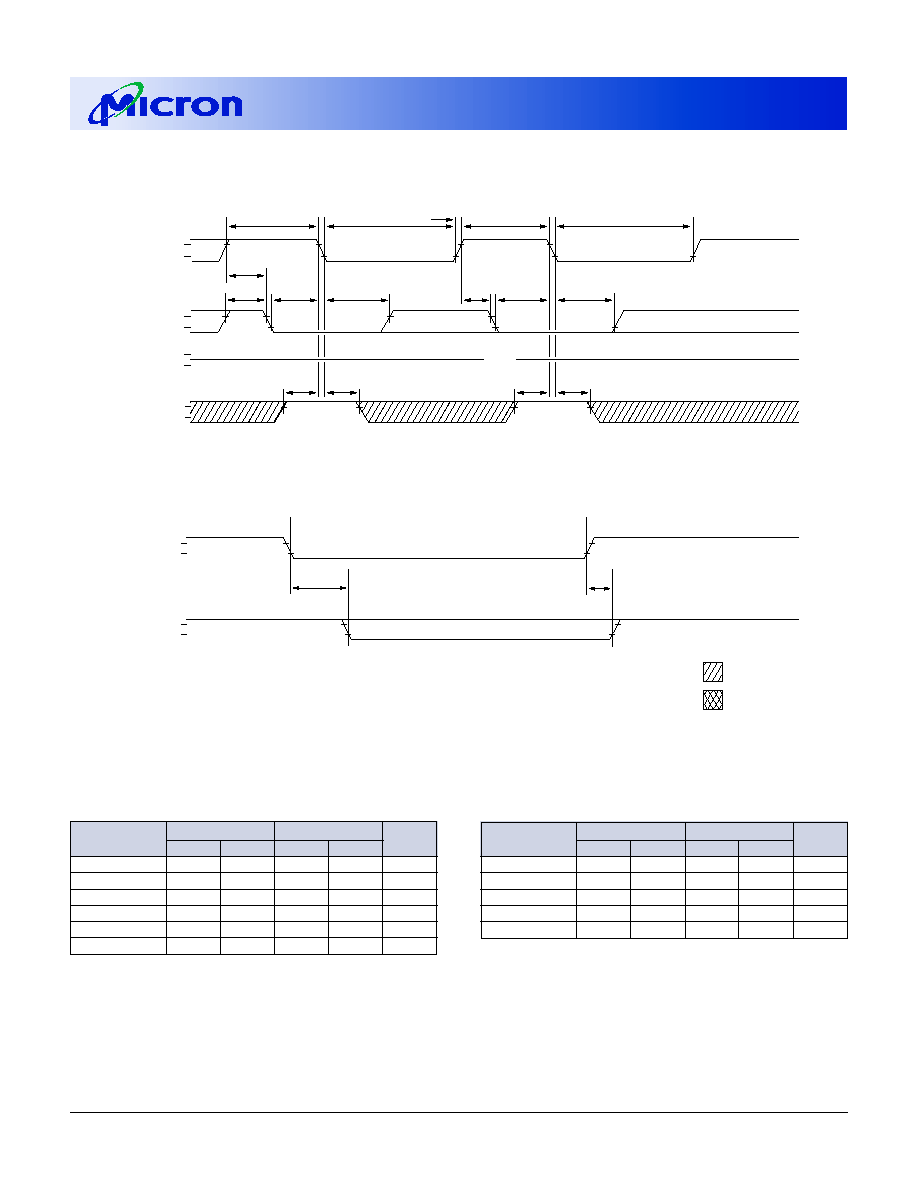
2, 4 Meg x 72 Buffered DRAM DIMMs
Micron Technology, Inc., reserves the right to change products or specifications without notice.
DM33.p65 ≠ Rev. 2/99
©1999, Micron Technology, Inc.
26
2, 4 MEG x 72
BUFFERED DRAM DIMMs
OBSOLETE
CBR REFRESH CYCLE
34
(Addresses, OE# = DON'T CARE)
PRESENCE-DETECT READ CYCLE
34
tPDOFF
PDE#
V
V
IH
IL
PD1-PD8
V
V
IH
IL
VALID PRESENCE-DETECT
tPD
DON'T CARE
UNDEFINED
tRP
V
V
IH
IL
RAS#
tRAS
NOTE 1
OPEN
tCHR
tCSR
V
V
IH
IL
V
V
OH
OL
CAS#
DQ
tRP
tRAS
tRPC
tCSR
tRPC
tCHR
tCP
V
V
IH
IL
tWRP
tWRH
WE#
tWRP
tWRH
NOTE: 1. PD pins must be pulled HIGH at next level of assembly.
t
RP
30
40
ns
t
RPC (FPM)
≠
0
ns
t
RPC (EDO)
5
5
ns
t
WRH
6
8
ns
t
WRP
10
12
ns
-5*
-6
SYMBOL
MIN
MAX
MIN
MAX
UNITS
FAST PAGE MODE AND EDO PAGE MODE
TIMING PARAMETERS
-5*
-6
SYMBOL
MIN
MAX
MIN
MAX
UNITS
t
CHR
6
8
ns
t
CP
8
10
ns
t
CSR
7
7
ns
t
PD
10
10
ns
t
PDOFF
2
2
ns
t
RAS
50
10,000
60
10,000
ns
*EDO version only

2, 4 Meg x 72 Buffered DRAM DIMMs
Micron Technology, Inc., reserves the right to change products or specifications without notice.
DM33.p65 ≠ Rev. 2/99
©1999, Micron Technology, Inc.
27
2, 4 MEG x 72
BUFFERED DRAM DIMMs
OBSOLETE
HIDDEN REFRESH CYCLE
20, 34
(WE# = HIGH; OE# = LOW)
DON'T CARE
UNDEFINED
tCLZ
tOFF
OPEN
VALID DATA
OPEN
COLUMN
ROW
tCAC
tRAC
tAA
tCAH
tASC
tRAH
tASR
tRAD
tAR
tCRP
tRCD
tRSH
tRAS
tRC
tRP
tCHR
tRAS
DQ
V
V
IOH
IOL
V
V
IH
IL
ADDR
V
V
IH
IL
CAS#
V
V
IH
IL
RAS#
t
OFF (FPM)
≠
≠
5
20
ns
t
OFF (EDO)
2
17
2
20
ns
t
ORD
0
0
ns
t
RAC
50
60
ns
t
RAD (FPM)
≠
13
ns
t
RAD (EDO)
7
10
ns
t
RAH
7
8
ns
t
RAS
50
10,000
60
10,000
ns
t
RCD (FPM)
≠
18
ns
t
RCD (EDO)
9
12
ns
t
RP
30
40
ns
t
RSH
18
20
ns
-5*
-6
SYMBOL
MIN
MAX
MIN
MAX
UNITS
FAST PAGE MODE AND EDO PAGE MODE
TIMING PARAMETERS
-5*
-6
SYMBOL
MIN
MAX
MIN
MAX
UNITS
t
AA
30
35
ns
t
AR
36
43
ns
t
ASC
2
2
ns
t
ASR
5
5
ns
t
CAC
18
20
ns
t
CAH
13
15
ns
t
CHR
6
8
ns
t
CLZ (FPM)
≠
5
ns
t
CLZ (EDO)
2
2
ns
t
CRP
10
10
ns
t
OD (FPM)
≠
≠
3
15
ns
t
OD (EDO)
0
12
0
15
ns
t
OE
12
15
ns
*EDO version only
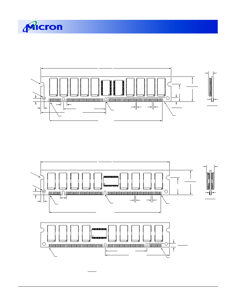
2, 4 Meg x 72 Buffered DRAM DIMMs
Micron Technology, Inc., reserves the right to change products or specifications without notice.
DM33.p65 ≠ Rev. 2/99
©1999, Micron Technology, Inc.
28
2, 4 MEG x 72
BUFFERED DRAM DIMMs
OBSOLETE
.350 (8.89)
MAX
.054 (1.37)
.046 (1.17)
1.005 (25.53)
.995 (25.27)
PIN 1
5.256 (133.50)
5.244 (133.20)
.700 (17.78)
TYP
.118 (3.00)
(2X)
.118 (3.00) TYP
.250 (6.35) TYP
4.550 (115.57)
.050 (1.27)
TYP
.118 (3.00)
TYP
.039 (1.00)
TYP
2.625 (66.68)
1.700 (43.18)
.079 (2.00) R
(2X)
.039 (1.00) R(2X)
PIN 84
FRONT VIEW
BACK VIEW
PIN 168
PIN 85
.128 (3.25)
.118 (3.00)
(2X)
168-PIN DIMM
DF-7 (32MB)
168-PIN DIMM
DF-8 (16MB)
.200 (5.08)
MAX
.054 (1.37)
.046 (1.17)
PIN 1 (PIN 85 on backside)
.700 (17.78)
TYP
.118 (3.00)
(2X)
.118 (3.00) TYP
.250 (6.35) TYP
4.550 (115.57)
.050 (1.27)
TYP
.118 (3.00) TYP
.039 (1.00)
TYP
.079 (2.00) R
(2X)
.039 (1.00) R(2X)
FRONT VIEW
.128 (3.25)
.118 (3.00)
PIN 84 (PIN 168 ON BACKSIDE)
(2X)
1.700 (43.18)
2.625 (66.68)
1.005 (25.53)
.995 (25.27)
5.256 (133.50)
5.244 (133.20)
NOTE: All dimensions in inches (millimeters) MAX or typical where noted.
MIN

2, 4 Meg x 72 Buffered DRAM DIMMs
Micron Technology, Inc., reserves the right to change products or specifications without notice.
DM33.p65 ≠ Rev. 2/99
©1999, Micron Technology, Inc.
29
2, 4 MEG x 72
BUFFERED DRAM DIMMs
OBSOLETE
8000 S. Federal Way, P.O. Box 6, Boise, ID 83707-0006, Tel: 208-368-3900
E-mail: prodmktg@micronsemi.com, Internet: http://www.micronsemi.com, Customer Comment Line: 800-932-4992
Micron is a registered trademark of Micron Technology, Inc.