PRODUCTS AND SPECIFICATIONS DISCUSSED HEREIN ARE FOR EVALUATION AND REFERENCE PURPOSES ONLY AND ARE SUBJECT TO CHANGE BY
MICRON WITHOUT NOTICE. PRODUCTS ARE ONLY WARRANTED BY MICRON TO MEET MICRON'S PRODUCTION DATA SHEET SPECIFICATIONS.
64, 128 Meg x72 SDRAM DIMM
Micron Technology, Inc., reserves the right to change products or specifications without notice.
SD9_18C64_128X72AG_A.fm - Rev. A 11/02 EN
1
©2002, Micron Technology Inc.
512MB / 1GB (x72)
168-PIN SDRAM DIMM
ADVANCE
SYNCHRONOUS
DRAM MODULE
MT9LSDT6472A - 512MB
MT18LSDT12872A - 1GB
For the latest data sheet, please refer to the Micron
‚
Web
site:
www.micron.com/moduleds
Features
∑ PC100- and PC133-compliant
∑ JEDEC-standard 168-pin, dual in-line memory
module (DIMM)
∑ Unbuffered, ECC-optimized pinout
∑ 512MB (64 Meg x 72) and 1GB (128 Meg x 72)
∑ Single +3.3V power supply
∑ Fully synchronous; all signals registered on positive
Edge of system clock
∑ Internal pipelined operation; column address can
be changed every clock cycle
∑ Internal SDRAM banks for hiding row access/precharge
∑ Programmable burst lengths: 1, 2, 4, 8, or full page
∑ Auto Precharge, includes Concurrent Auto
Precharge, and Auto Refresh Modes
∑ Self Refresh Mode
∑ 64ms, 8,192-cycle refresh
∑ LVTTL-compatible inputs and outputs
∑ Serial Presence-Detect (SPD)
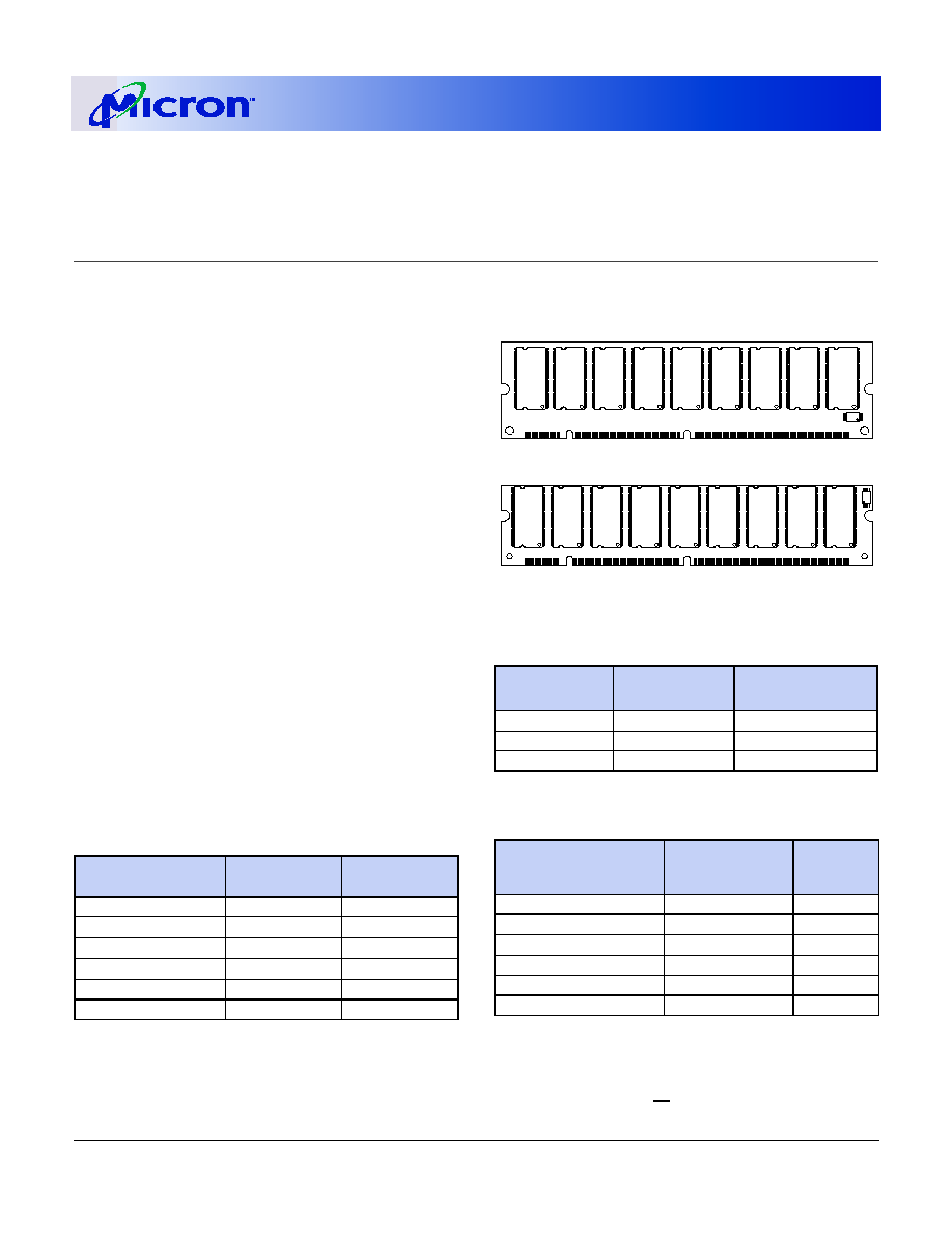
Figure 1: 168-PIN DIMM (MO-161)
OPTIONS
MARKING
∑ Package
168-pin DIMM (gold)
G
∑ Frequency/CAS Latency
7.5ns (133 MHz)/CL = 2
-13E
7.5ns (133 MHz)/CL = 3
-133
10ns (100 MHz)/CL = 2
-10E
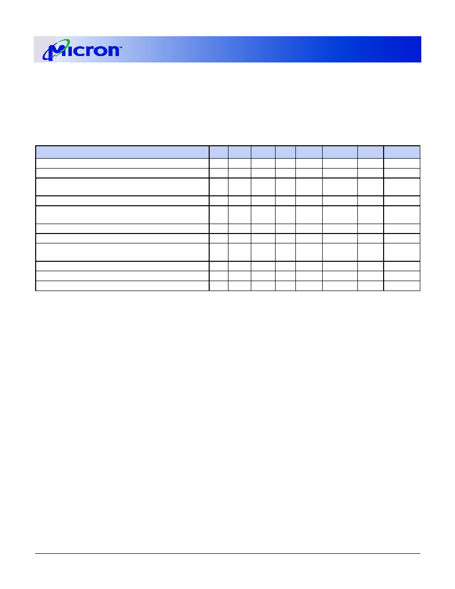
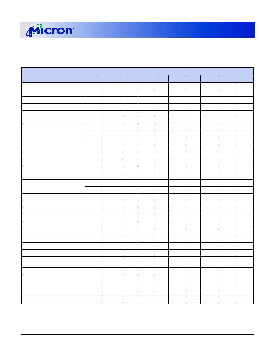
Table 1:
Address Table
512MB
MODULE
1GB
MODULE
Refresh Count
8K
8K
Device Banks
4 (BA0, BA1)
4 (BA0, BA1)
Device Configuration
64 Meg x 8
64 Meg x 8
Row Addressing
8K (A0≠A12)
8K (A0≠A12)
Column Addressing
2K (A0≠A9, A11) 2K (A0≠A9, A11)
Module Banks
1 (S0,S2)
2 (S0,S2; S1,S3)
Table 2:
Timing parameters
MODULE
MARKINGS
PC100
CL -
t
RCD -
t
RP
PC133
CL -
t
RCD -
t
RP
-13E
2 - 2 - 2
2 - 2 - 2
-133
2 - 2 - 2
3 - 3 - 3
-10E
2 - 2 - 2
NA
Table 3:
Part Numbers
PARTNUMBER
1
NOTE:
1. The designators for component and PCB revision
are the last two characters of each part number
Consult factory for current revision codes. Example:
MT9LSDT6472AG-133B1.
CONFIGURATION
SYSTEM
BUS
SPEED
MT9LSDT6472AG-13E_
64 Meg x 72
133 MHz
MT9LSDT6472AG-133_
64 Meg x 72
133 MHz
MT9LSDT6472AG-10E_
64 Meg x 72
100 MHz
MT18LSDT12872AG-13E_
128 Meg x 72
133 MHz
MT18LSDT12872AG-133_
128 Meg x 72
133 MHz
MT18LSDT12872AG-10E_
128 Meg x 72
100 MHz
Standard
Low Profile
512MB / 1GB (x72)
168-PIN SDRAM DIMM
ADVANCE
64, 128 Meg x72 SDRAM DIMM
Micron Technology, Inc., reserves the right to change products or specifications without notice.
SD9_18C64_128X72AG_A.fm - Rev. A 11/02 EN
2
©2002, Micron Technology Inc.
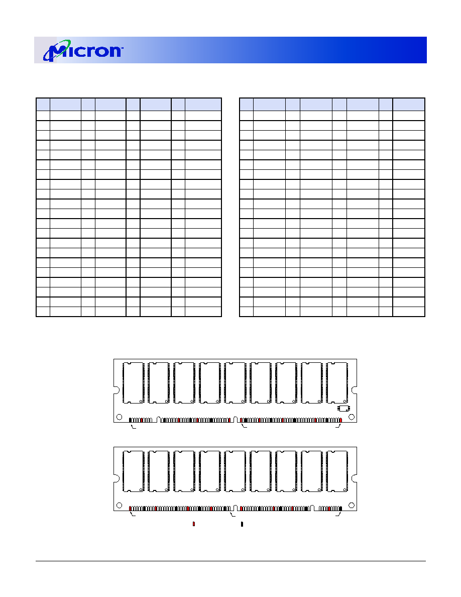
Figure 2: Pin Locations (168-Pin DIMM)
PIN Locations (168-PIN Low Profile DIMM)
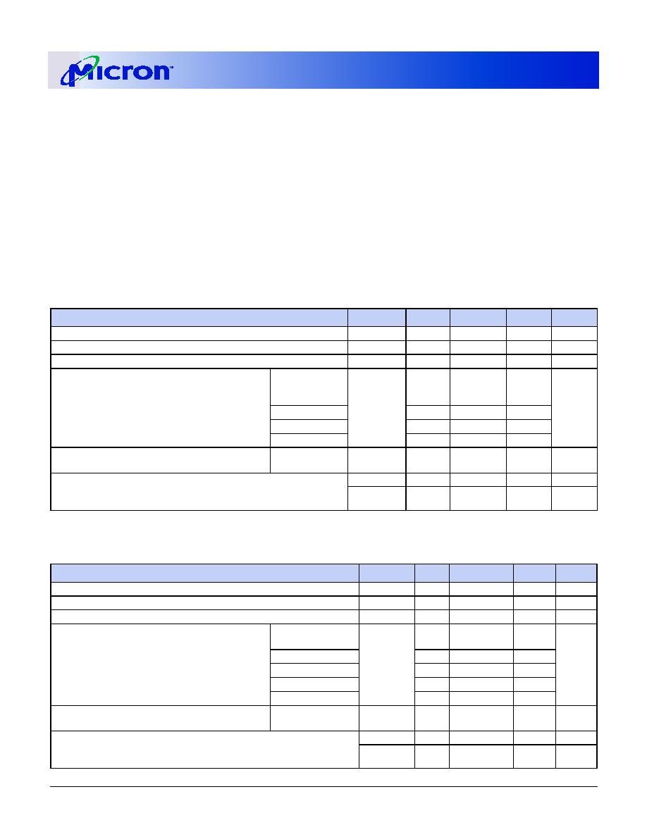
Table 4:
Pin Assignment
(168-Pin DIMM Front)
PIN SYMBOL PIN SYMBOL PIN SYMBOL PIN SYMBOL
1
V
SS
22
CB1
43
V
SS
64
V
SS
2
DQ0
23
V
SS
44
NC
65
DQ21
3
DQ1
24
NC
45
S2#
66
DQ22
4
DQ2
25
NC
46
DQMB2
67
DQ23
5
DQ3
26
V
DD
47
DQMB3
68
V
SS
6
V
DD
27
WE#
48
NC
69
DQ24
7
DQ4
28 DQMB0
49
V
DD
70
DQ25
8
DQ5
29 DQMB1
50
NC
71
DQ26
9
DQ6
30
S0#
51
NC
72
DQ27
10
DQ7
31
NC
52
CB2
73
V
DD
11
DQ8
32
V
SS
53
CB3
74
DQ28
12
V
SS
33
A0
54
V
SS
75
DQ29
13
DQ9
34
A2
55
DQ16
76
DQ30
14
DQ10
35
A4
56
DQ17
77
DQ31
15
DQ11
36
A6
57
DQ18
78
V
SS
16
DQ12
37
A8
58
DQ19
79
CK2
17
DQ13
38
A10
59
V
DD
80
NC
18
V
DD
39
BA1
60
DQ20
81
NC
19
DQ14
40
V
DD
61
NC
82
SDA
20
DQ15
41
V
DD
62
NC
83
SCL
21
CB0
42
CK0
63
CKE1
84
V
DD
Table 5:
Pin Assignment
(168-Pin DIMM Back)
PIN SYMBOL PIN SYMBOL PIN SYMBOL PIN SYMBOL
85
V
SS
106
CB5
127
V
SS
148
V
SS
86
DQ32
107
V
SS
128
CKE0
149
DQ53
87
DQ33
108
NC
129
S3#
150
DQ54
88
DQ34
109
NC
130 DQMB6
151
DQ55
89
DQ35
110
V
DD
131 DQMB7 152
V
SS
90
V
DD
111
CAS#
132
NC
153
DQ56
91
DQ36
112 DQMB4 133
V
DD
154
DQ57
92
DQ37
113 DQMB5 134
NC
155
DQ58
93
DQ38
114
S1#
135
NC
156
DQ59
94
DQ39
115
RAS#
136
CB6
157
V
DD
95
DQ40
116
V
SS
137
CB7
158
DQ60
96
V
SS
117
A1
138
V
SS
159
DQ61
97
DQ41
118
A3
139
DQ48
160
DQ62
98
DQ42
119
A5
140
DQ49
161
DQ63
99
DQ43
120
A7
141
DQ50
162
V
SS
100
DQ44
121
A9
142
DQ51
163
CK3
101
DQ45
122
BA0
143
V
DD
164
NC
102
V
DD
123
A11
144
DQ52
165
SA0
103
DQ46
124
V
DD
145
NC
166
SA1
104
DQ47
125
CK1
146
NC
167
SA2
105
CB4
126
A12
147
NC
168
V
DD
Front View
Back View (Populated only for 1GB module)
Indicates a V
DD
pin
Indicates a V
SS
pin
PIN 1
PIN 41
PIN 84
PIN 85
PIN125
PIN 168
U1
U2
U3
U4
U5
U6
U7
U8
U9
U10
U11
U12
U13
U14
U15
U16
U17
U18
U19
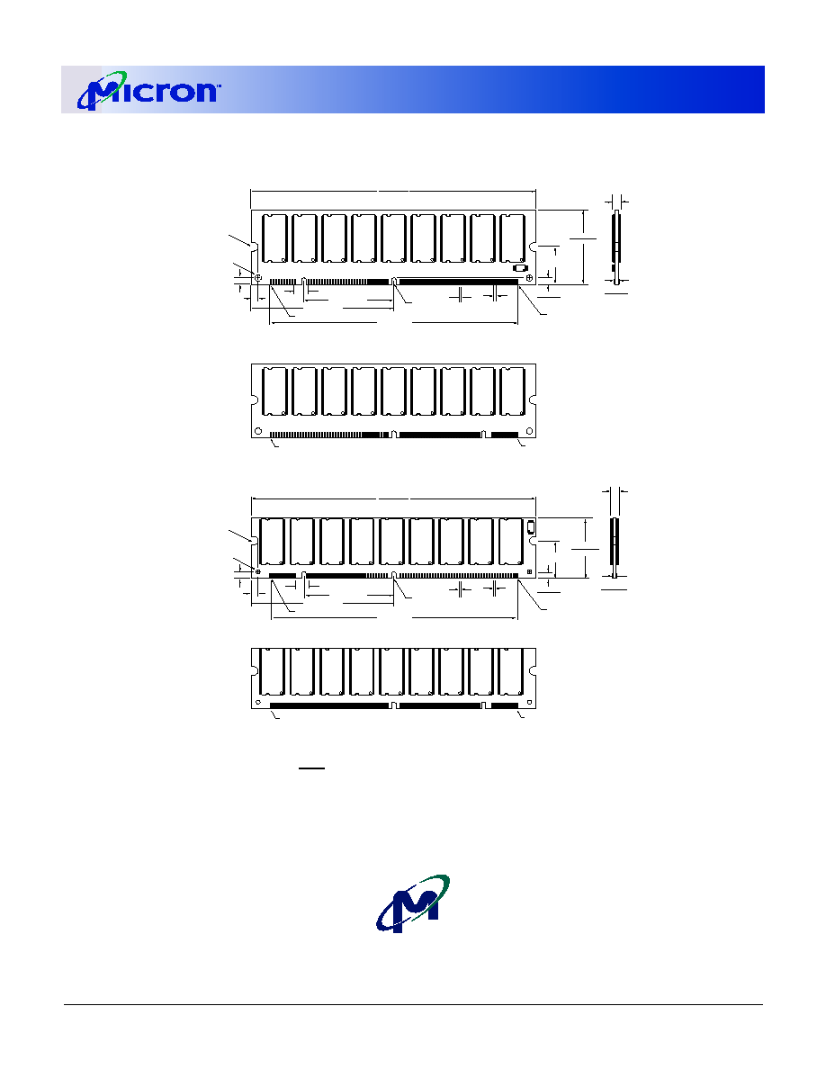
See Figure 11, 512MB Module Dimensions and Figure 12, 1GB Module Dimensions for module dimensions.
512MB / 1GB (x72)
168-PIN SDRAM DIMM
ADVANCE
64, 128 Meg x72 SDRAM DIMM
Micron Technology, Inc., reserves the right to change products or specifications without notice.
SD9_18C64_128X72AG_A.fm - Rev. A 11/02 EN
3
©2002, Micron Technology Inc.
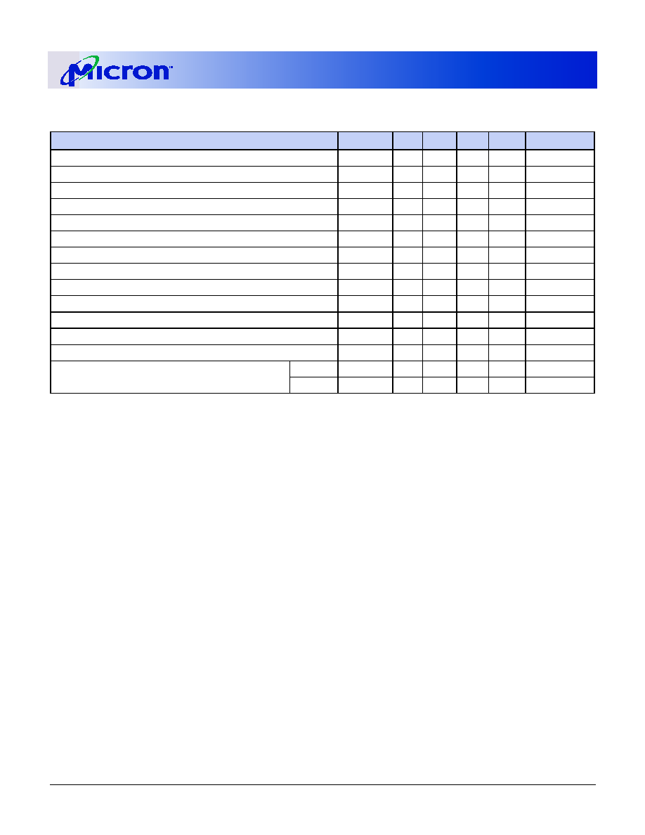
Table 6:
Pin Descriptions
Pin numbers may not correlate with symbols. Refer to the Pin Assignment table for pin number and symbol information
PIN NUMBERS
SYMBOL
TYPE
DESCRIPTION
27, 111, 115
RAS#, CAS#,
WE#
Input
Command Inputs: RAS#, CAS#, and WE# (along with S#)
define the command being entered.
42, 79, 125, 163
CK0-CK3
Input
Clock: CK is driven by the system clock. All SDRAM input signals are
sampled on the positive edge of CK. CK also increments the
internal burst counter and controls the output registers.
63, 128
CKE0, CKE1
Input
Clock Enable: CKE activates (HIGH) and deactivates (LOW) the CK
signal. Deactivating the clock provides PRECHARGE POWER-DOWN
and SELF REFRESH operation (all device banks idle) or CLOCK
SUSPEND OPERATION (burst access in progress). CKE is synchronous
except after the device enters power- down and self refresh modes,
where CKE becomes asynchronous until after exiting the same
mode. The input buffers, including CK, are disabled during power-
down and self refresh modes, providing low standby power.
30, 45,114, 129
S0# -S3#
Input
Chip Select: S# enables (registered LOW) and disables (registered
HIGH) the command decoder. All com- mands are masked when S#
is registered HIGH. S# is considered part of the command code.
28, 29, 46, 47, 112, 113, 130,
131
DQMB0-DQMB7
Input
Input/Output Mask: DQMB is an input mask signal for write
accesses and an output enable signal for read accesses. Input data
is masked when DQMB is sampled HIGH during a WRITE cycle. The
output buffers are placed in a High-Z state (two-clock latency)
when DQMB is sampled HIGH during a READ cycle.
39, 122
BA0, BA1
Input
Bank Address: BA0 and BA1 define to which device bank the
ACTIVE, READ, WRITE, or PRECHARGE command is being applied.
33 - 38, 117 - 121, 123, 126
A0-A12
Input
Address Inputs: Provide the row address for ACTIVE commands, and
the column address and auto prcharge bit (A10) for READ/WRITE
commands, to select one location out of the memory arrary in the
respective device bank. A10 sampled during a PRECHARGE command
determines whether the PRECHARGE applies to one device bank (A10
LOW< device bank selected by BA0, BA1) or all device banks (A10
HIGH). The address inputs also provide the op-code during a MODE
REGISTER SET command.
83
SCL
Input
Serial Clock for Presence-Detect: SCL is used to synchronize
the presence-detect data transfer to and from the module.
165-167
SA0-SA2
Input
Presence-Detect Address Inputs: These pins are used to
configure the presence-detect device.
21, 22, 52, 53, 105, 106, 136,
137
CB0-CB7
Input/
Output
Check Bits. ECC, 1-bit error detection and correction.
2-5, 7-11, 13-17, 19, 20, 55-58,
60, 65-67, 69-72, 74-77, 86-89,
91-95, 97-101, 103, 104,
139-142, 144, 149-151,
153-156,158-161
DQ0-DQ63
Input/
Output
Data I/O: Data bus.
82
SDA
Input/
Output
Serial Presence-Detect Data: SDA is a bidirectional pin used to
transfer addresses and data into and out of the presence-
detect portion of the module.
512MB / 1GB (x72)
168-PIN SDRAM DIMM
ADVANCE
64, 128 Meg x72 SDRAM DIMM
Micron Technology, Inc., reserves the right to change products or specifications without notice.
SD9_18C64_128X72AG_A.fm - Rev. A 11/02 EN
4
©2002, Micron Technology Inc.
6, 18, 26, 40, 41, 49, 59, 73,
84, 90, 102, 110, 124, 133,
143, 157, 168
V
DD
Supply
Power Supply: +3.3V ±0.3V.
1, 12, 23, 32, 43, 54, 64, 68,
78, 85, 96, 107, 116, 127, 138,
148, 152, 162
V
SS
Supply
Ground.
24, 25, 31, 44, 48, 50, 51 61,
62, 80, 81, 108, 109, 132, 134,
135, 145,146, 147
NC
≠
Not Connected: These pins are not connected on these
module.
Table 6:
Pin Descriptions (Continued)
Pin numbers may not correlate with symbols. Refer to the Pin Assignment table for pin number and symbol information
PIN NUMBERS
SYMBOL
TYPE
DESCRIPTION
512MB / 1GB (x72)
168-PIN SDRAM DIMM
ADVANCE
64, 128 Meg x72 SDRAM DIMM
Micron Technology, Inc., reserves the right to change products or specifications without notice.
SD9_18C64_128X72AG_A.fm - Rev. A 11/02 EN
5
©2002, Micron Technology Inc.
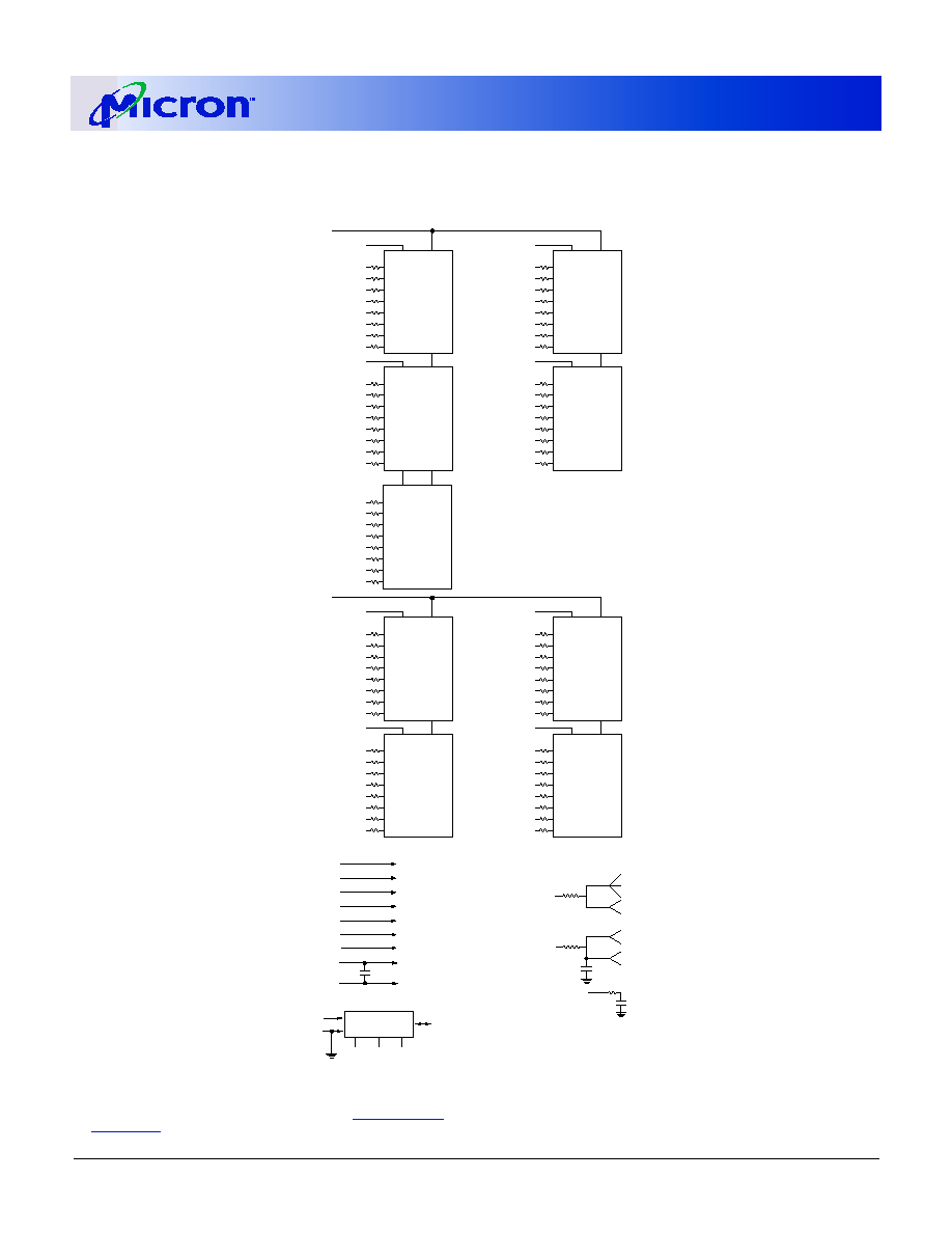
Figure 3: Functional Block Diagram
Single Bank Module
DQM CS#
U8
A0
SA0
SPD
SDA
A1
SA1
A2
SA2
DQ56
DQ57
DQ58
DQ59
DQ60
DQ61
DQ62
DQ63
DQMB7
DQM CS#
U6
DQ48
DQ49
DQ50
DQ51
DQ52
DQ53
DQ54
DQ55
DQMB6
DQM CS#
U4
DQ40
DQ41
DQ42
DQ43
DQ44
DQ45
DQ46
DQ47
DQMB5
DQM CS#
U2
DQ32
DQ33
DQ34
DQ35
DQ36
DQ37
DQ38
DQ39
DQMB4
DQM CS#
U9
DQ24
DQ25
DQ26
DQ27
DQ28
DQ29
DQ30
DQ31
DQMB3
DQM CS#
U7
DQ16
DQ17
DQ18
DQ19
DQ20
DQ21
DQ22
DQ23
DQMB2
DQM CS#
U3
DQ8
DQ9
DQ10
DQ11
DQ12
DQ13
DQ14
DQ15
DQMB1
DQM CS#
U1
DQ
DQ
DQ
DQ
DQ
DQ
DQ
DQ
DQ0
DQ1
DQ2
DQ3
DQ4
DQ5
DQ6
DQ7
DQMB0
S2#
S0#
RAS#
CAS#
CKE0
WE#
RAS#: SDRAMs
CAS#: SDRAMs
CKE0: SDRAMs
WE#: SDRAMs
A0-A11: SDRAMs
BA0: SDRAMs
BA1: SDRAMs
A0-A11
BA0
BA1
DQM CS#
U5
CB0
CB1
CB2
CB3
CB4
CB5
CB6
CB7
V
DD
V
SS
SDRAMs
SDRAMs
10pF
CK1, CK3
U1
U2
U3
U4
U5
CK0
U6
U7
U8
U9
CK2
3.3pF
SCL
WP
U10
DQ
DQ
DQ
DQ
DQ
DQ
DQ
DQ
DQ
DQ
DQ
DQ
DQ
DQ
DQ
DQ
DQ
DQ
DQ
DQ
DQ
DQ
DQ
DQ
DQ
DQ
DQ
DQ
DQ
DQ
DQ
DQ
DQ
DQ
DQ
DQ
DQ
DQ
DQ
DQ
DQ
DQ
DQ
DQ
DQ
DQ
DQ
DQ
DQ
DQ
DQ
DQ
DQ
DQ
DQ
DQ
DQ
DQ
DQ
DQ
DQ
DQ
DQ
DQ
Note:
1. All resistor values are 10
W unless otherwise specified.
2. Per industry standard, Micron modules use various component speed grades as
referenced in the module part numbering guide at
www.micron.com/
numberguide
.
SDRAMs = MT48LC64M8A2TG
512MB / 1GB (x72)
168-PIN SDRAM DIMM
ADVANCE
64, 128 Meg x72 SDRAM DIMM
Micron Technology, Inc., reserves the right to change products or specifications without notice.
SD9_18C64_128X72AG_A.fm - Rev. A 11/02 EN
6
©2002, Micron Technology Inc.
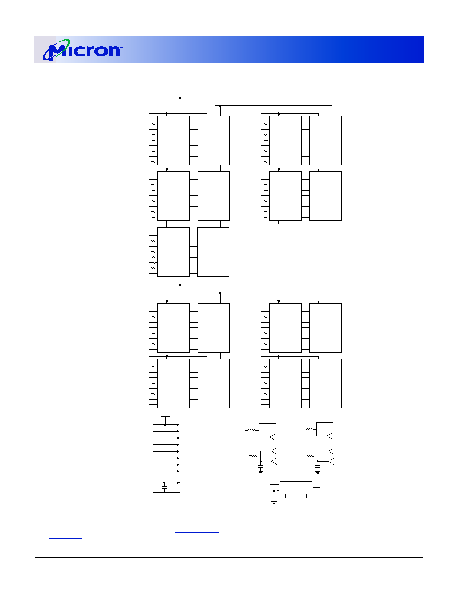
Figure 4: Functional Block Diagram
Dual Bank Module
DQM CS#
U8
DQ56
DQ57
DQ58
DQ59
DQ60
DQ61
DQ62
DQ63
DQMB7
DQM CS#
U6
DQ48
DQ49
DQ50
DQ51
DQ52
DQ53
DQ54
DQ55
DQMB6
DQM CS#
U4
DQ40
DQ41
DQ42
DQ43
DQ44
DQ45
DQ46
DQ47
DQMB5
DQM CS#
U2
DQ32
DQ33
DQ34
DQ35
DQ36
DQ37
DQ38
DQ39
DQMB4
DQM CS#
U9
DQ24
DQ25
DQ26
DQ27
DQ28
DQ29
DQ30
DQ31
DQMB3
DQM CS#
U7
DQ16
DQ17
DQ18
DQ19
DQ20
DQ21
DQ22
DQ23
DQMB2
DQM CS#
U3
DQ8
DQ9
DQ10
DQ11
DQ12
DQ13
DQ14
DQ15
DQMB1
DQM CS#
U1
DQ
DQ
DQ
DQ
DQ
DQ
DQ
DQ
DQ0
DQ1
DQ2
DQ3
DQ4
DQ5
DQ6
DQ7
DQMB0
S2#
S0#
DQM CS#
U5
CB0
CB1
CB2
CB3
CB4
CB5
CB6
CB7
DQM CS#
U12
DQM CS#
U14
DQM CS#
U16
DQM CS#
U18
S1#
DQM CS#
U11
DQM CS#
U13
DQM CS#
U17
DQM CS#
U19
DQM CS#
U15
S3#
A0
SA0
SPD
SDA
A1
SA1
A2
SA2
CKE1
CKE0
CAS#
RAS#
WE#
CKE: SDRAMs U11-U19
CKE: SDRAMs U1-U9
CAS#: SDRAMs
RAS#: SDRAMs
WE#: SDRAMs
A0-A11: SDRAMs
BA0: SDRAMs
BA1: SDRAMs
A0-A11
BA0
BA1
V
DD
V
SS
SDRAMs
SDRAMs
V
DD
10K
SCL
WP
U10
U1
U2
U3
U4
U5
CK0
U6
U7
U8
U9
CK2
3.3pF
U11
U12
U13
U14
CK3
3.3pF
U15
U16
U17
U18
U19
CK1
DQ
DQ
DQ
DQ
DQ
DQ
DQ
DQ
DQ
DQ
DQ
DQ
DQ
DQ
DQ
DQ
DQ
DQ
DQ
DQ
DQ
DQ
DQ
DQ
DQ
DQ
DQ
DQ
DQ
DQ
DQ
DQ
DQ
DQ
DQ
DQ
DQ
DQ
DQ
DQ
DQ
DQ
DQ
DQ
DQ
DQ
DQ
DQ
DQ
DQ
DQ
DQ
DQ
DQ
DQ
DQ
DQ
DQ
DQ
DQ
DQ
DQ
DQ
DQ
DQ
DQ
DQ
DQ
DQ
DQ
DQ
DQ
DQ
DQ
DQ
DQ
DQ
DQ
DQ
DQ
DQ
DQ
DQ
DQ
DQ
DQ
DQ
DQ
DQ
DQ
DQ
DQ
DQ
DQ
DQ
DQ
DQ
DQ
DQ
DQ
DQ
DQ
DQ
DQ
DQ
DQ
DQ
DQ
DQ
DQ
DQ
DQ
DQ
DQ
DQ
DQ
DQ
DQ
DQ
DQ
DQ
DQ
DQ
DQ
DQ
DQ
DQ
DQ
DQ
DQ
DQ
DQ
DQ
DQ
DQ
DQ
Note:
1. All resistor values are 10
W unless otherwise specified.
2. Per industry standard, Micron modules use various component speed grades as
referenced in the module part numbering guide at
www.micron.com/
numberguide
.
SDRAMs = MT48LC64M8A2TG

512MB / 1GB (x72)
168-PIN SDRAM DIMM
ADVANCE
64, 128 Meg x72 SDRAM DIMM
Micron Technology, Inc., reserves the right to change products or specifications without notice.
SD9_18C64_128X72AG_A.fm - Rev. A 11/02 EN
7
©2002, Micron Technology Inc.
General Description
The MT9LSDT6472A and MT18LSDT12872A mod-
ules are high-speed CMOS, dynamic random-access,
512MB and 1GB DIMMs organized in a x72 configura-
tion. These modules use internally configured quad-
bank SDRAMs with a synchronous interface (all signals
are registered on the positive edge of the clock signal
CK).
Read and write accesses to the SDRAM modules are
burst oriented; accesses start at a selected location and
continue for a programmed number of locations in a
programmed sequence. Accesses begin with the regis-
tration of an ACTIVE command, which is then fol-
lowed by a READ or WRITE command. The address
bits registered coincident with the ACTIVE command
are used to select the device bank and row to be
accessed (BA0, BA1 select the device bank, A0≠A12
select the device row). The address bits registered
coincident with the READ or WRITE command are
used to select the starting column location for the
burst access.
These modules provide for programmable READ or
WRITE burst lengths of 1, 2, 4, or 8 locations, or the full
page, with a burst terminate option. An AUTO PRE-
CHARGE function may be enabled to provide a self-timed
row precharge that is initiated at the end of the burst
sequence.
These modules use an internal pipelined architec-
ture to achieve high-speed operation. This architec-
ture is compatible with the 2n rule of prefetch
architectures, but it also allows the column address to
be changed on every clock cycle to achieve a high-
speed, fully random access. Precharging one device
bank while accessing one of the other three device
banks will hide the precharge cycles and provide
seamless, high-speed, random-access operation.
The modules are designed to operate in 3.3V, low-
power memory systems. An auto refresh mode is pro-
vided, along with a power-saving, power-down mode.
All inputs and outputs are LVTTL-compatible.
SDRAM modules offer substantial advances in
DRAM operating performance, including the ability to
syn-chronously burst data at a high data rate with
automatic column-address generation, the ability to
interleave between internal device banks in order to
hide precharge time and the capability to randomly
change column addresses on each clock cycle during a
burst access. For more information regarding SDRAM
operation, refer to the 512Mb SDRAM component data
sheet.
Serial Presence-Detect Operation
These modules incorporate serial presence-detect
(SPD). The SPD function is implemented using a
2,048-bit EEPROM. This nonvolatile storage device
contains 256 bytes. The first 128 bytes can be pro-
grammed by Micron to identify the module type and
various SDRAM organizations and timing parameters.
The remaining 128 bytes of storage are available for
use by the customer. System READ/WRITE operations
between the master (system logic) and the slave
EEPROM device (DIMM) occur via a standard I
2
C bus
using the DIMM's SCL (clock) and SDA (data) signals,
together with SA (2:0), which provide eight unique
DIMM/EEPROM addresses.
SDRAM Functional Description
In general, the 512Mb SDRAMs are quad-bank
DRAMs that operate at 3.3V and include a synchro-
nous interface (all signals are registered on the positive
edge of the clock signal, CK). The four banks of the x8
configured devices used for these modules are config-
ured as 8,192 bit-rows by 2,048 bit-columns, by 8
input/output bits.
Read and write accesses to the SDRAM are burst ori-
ented; accesses start at a selected location and con-
tinue for a programmed number of locations in a
programmed sequence. Accesses begin with the regis-
tration of an ACTIVE command, which is then fol-
lowed by a READ or WRITE command. The address
bits registered coincident with the ACTIVE command
are used to select the device bank and row to be
accessed; BA0 and BA1 select the device bank, A0≠A12
select the device row. The address bits A0≠A9 regis-
tered coincident with the READ or WRITE command
are used to select the starting column location for the
burst access.
Prior to normal operation, the SDRAM must be ini-
tialized. The following sections provide detailed infor-
mation covering device initialization, register
definition, command descriptions and device opera-
tion.
Initialization
SDRAMs must be powered up and initialized in a
predefined manner. Operational procedures other
than those specified may result in undefined opera-
tion. Once power is applied to V
DD
and V
DD
Q (simul-
taneously) and the clock is stable (stable clock is
defined as a signal cycling within timing constraints
specified for the clock pin), the SDRAM requires a
100µs delay prior to issuing any command other than a
COMMAND INHIBIT or NOP. Starting at some point

512MB / 1GB (x72)
168-PIN SDRAM DIMM
ADVANCE
64, 128 Meg x72 SDRAM DIMM
Micron Technology, Inc., reserves the right to change products or specifications without notice.
SD9_18C64_128X72AG_A.fm - Rev. A 11/02 EN
8
©2002, Micron Technology Inc.
during this 100µs period and continuing at least
through the end of this period, COMMAND INHIBIT
or NOP commands should be applied.
Once the 100µs delay has been satisfied with at least
one COMMAND INHIBIT or NOP command having
been applied, a PRECHARGE command should be
applied. All device banks must then be precharged,
thereby placing the device in the all banks idle state.
Once in the idle state, two AUTO REFRESH cycles
must be performed. After the AUTO REFRESH cycles
are complete, the SDRAM is ready for mode register
programming. Because the mode register will power
up in an unknown state, it should be loaded prior to
applying any operational command.
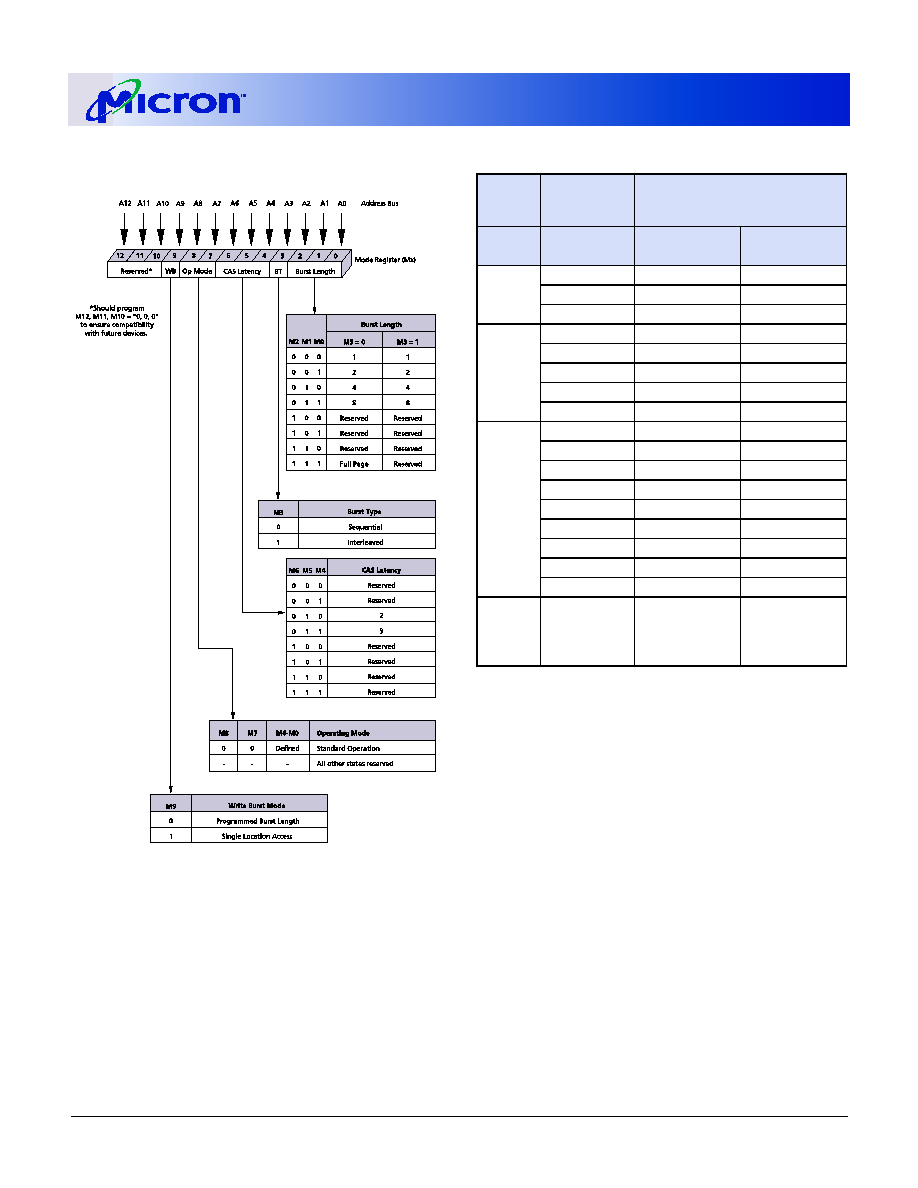
Mode Register Definition
The mode register is used to define the specific
mode of operation of the SDRAM. This definition
includes the selection of a burst length, a burst type, a
CAS latency, an operating mode and a write burst
mode, as shown in Figure 5, Mode Register Definition
Diagram. The mode register is programmed via the
LOAD MODE REGISTER command and will retain the
stored information until it is programmed again or the
device loses power.
Mode register bits M0≠M2 specify the burst length,
M3 specifies the type of burst (sequential or inter-
leaved), M4≠M6 specify the CAS latency, M7 and M8
specify the operating mode, M9 specifies the write
burst mode, and M10 and M11 are reserved for future
use. Address A12 (M12) is undefined but should be
driven LOW during loading of the mode register.
The mode register must be loaded when all device
banks are idle, and the controller must wait the speci-
fied time before initiating the subsequent operation.
Violating either of these requirements will result in
unspecified operation.
Burst Length
Read and write accesses to the SDRAM are burst ori-
ented, with the burst length being programmable, as
shown in Figure 5, Mode Register Definition Diagram.
The burst length determines the maximum number of
column locations that can be accessed for a given
READ or WRITE command. Burst lengths of 1, 2, 4, or 8
locations are available for both the sequential and the
interleaved burst types, and a full-page burst is avail-
able for the sequential type. The full-page burst is used
in conjunction with the BURST TERMINATE com-
mand to generate arbitrary burst lengths.
Reserved states should not be used, as unknown
operation or incompatibility with future versions may
result.
When a READ or WRITE command is issued, a block
of columns equal to the burst length is effectively
selected. All accesses for that burst take place within
this block, meaning that the burst will wrap within the
block if a boundary is reached, as shown in the Burst
Definition Table. The block is uniquely selected by A1≠
A9, A11 when the burst length is set to two; A2≠A9, A11
when the burst length is set to four; and by A3≠A9, A11
when the burst length is set to eight. The remaining
(least significant) address bit(s) is (are) used to select
the starting location within the block. Full-page bursts
wrap within the page if the boundary is reached, as
shown in Table 7, Burst Definition Table, on page 9.
Burst Type
Accesses within a given burst may be programmed
to be either sequential or interleaved; this is referred to
as the burst type and is selected via bit M3.
The ordering of accesses within a burst is deter-
mined by the burst length, the burst type and the start-
ing column address, as shown in Table 7, Burst
Definition Table, on page 9.
512MB / 1GB (x72)
168-PIN SDRAM DIMM
ADVANCE
64, 128 Meg x72 SDRAM DIMM
Micron Technology, Inc., reserves the right to change products or specifications without notice.
SD9_18C64_128X72AG_A.fm - Rev. A 11/02 EN
9
©2002, Micron Technology Inc.
Figure 5: Mode Register Definition
Diagram
NOTE:
1. For full-page accesses: y = 2,048
2. For a burst length of two, A1
≠
A9, A11 select the
block of two burst; A0 selects the starting column
within the block.
3. For a burst length of four, A2
≠
A9, A11 select the
block of four burst; A0
≠
A1 select the starting col-
umn within the block.
4. For a burst length of eight, A3
≠
A9, A11 select the
block of eight burst; A0
≠
A2 select the starting col-
umn within the block.
5. For a full-page burst, the full row is selected and
A0
≠
A9, A11 select the starting column.
6. Whenever a boundary of the block is reached
within a given sequence above, the following
access wraps within the block.
7. For a burst length of one, A0
≠
A9, A11 select the
unique column to be accessed, and Mode Register
bit M3 is ignored.
Table 7:
Burst Definition Table
BURST
LENGTH
STARTING
COLUMN
ADDRESS
ORDER OF ACCESSES WITHIN
A BURST
TYPE =
SEQUENTIAL
TYPE =
INTERLEAVED
2
A0
0
0-1
0-1
1
1-0
1-0
4
A1
A0
0
0
0-1-2-3
0-1-2-3
0
1
1-2-3-0
1-0-3-2
1
0
2-3-0-1
2-3-0-1
1
1
3-0-1-2
3-2-1-0
8
A2 A1
A0
0
0
0
0-1-2-3-4-5-6-7
0-1-2-3-4-5-6-7
0
0
1
1-2-3-4-5-6-7-0
1-0-3-2-5-4-7-6
0
1
0
2-3-4-5-6-7-0-1
2-3-0-1-6-7-4-5
0
1
1
3-4-5-6-7-0-1-2
3-2-1-0-7-6-5-4
1
0
0
4-5-6-7-0-1-2-3
4-5-6-7-0-1-2-3
1
0
1
5-6-7-0-1-2-3-4
5-4-7-6-1-0-3-2
1
1
0
6-7-0-1-2-3-4-5
6-7-4-5-2-3-0-1
1
1
1
7-0-1-2-3-4-5-6
7-6-5-4-3-2-1-0
Full
Page
(y)
n= A0
≠
A9,
A11
(location 0-y)
Cn, Cn+1, Cn+2
Cn+3, Cn+4...
...Cn-1,
Cn...
Not Supported
512MB / 1GB (x72)
168-PIN SDRAM DIMM
ADVANCE
64, 128 Meg x72 SDRAM DIMM
Micron Technology, Inc., reserves the right to change products or specifications without notice.
SD9_18C64_128X72AG_A.fm - Rev. A 11/02 EN
10
©2002, Micron Technology Inc.
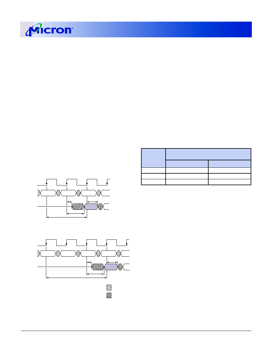
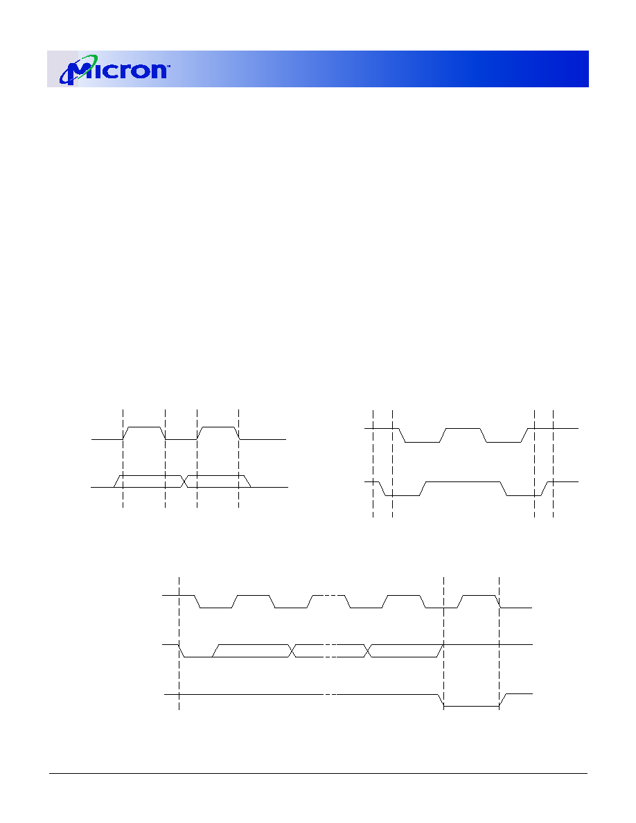
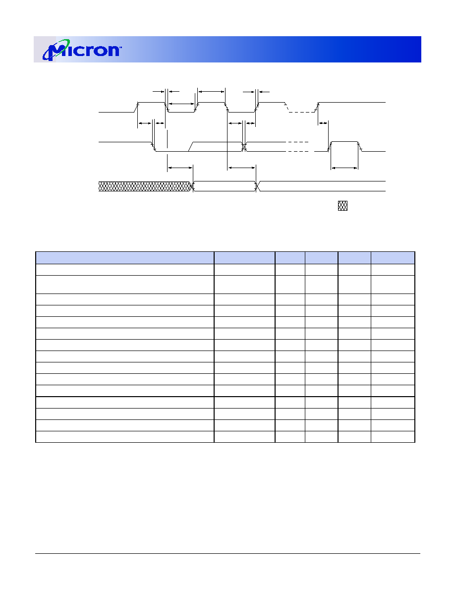
CAS Latency
The CAS latency is the delay, in clock cycles,
between the registration of a READ command and the
availability of the first piece of output data. The latency
can be set to two or three clocks.
If a READ command is registered at clock edge n,
and the latency is m clocks, the data will be available
by clock edge n + m. The DQs will start driving as a
result of the clock edge one cycle earlier (n + m - 1),
and provided that the relevant access times are met,
the data will be valid by clock edge n + m. For example,
assuming that the clock cycle time is such that all rele-
vant access times are met, if a READ command is reg-
istered at T0 and the latency is programmed to two
clocks, the DQs will start driving after T1 and the data
will be valid by T2, as shown in Figure 6, CAS Latency
Diagram. Table 8, CAS Latency Table, indicates the
operating frequencies at which each CAS latency set-
ting can be used.
Reserved states should not be used as unknown
operation or incompatibility with future versions may
result.
Figure 6: CAS Latency Diagram
Operating Mode
The normal operating mode is selected by setting
M7 and M8 to zero; the other combinations of values
for M7 and M8 are reserved for future use and/or test
modes. The programmed burst length applies to both
READ and WRITE bursts.
Test modes and reserved states should not be used
because unknown operation or incompatibility with
future versions may result.
Write Burst Mode
When M9 = 0, the burst length programmed via M0-
M2 applies to both READ and WRITE bursts; when M9
= 1, the programmed burst length applies to READ
bursts, but write accesses are single-location (non-
burst) accesses.
CLK
DQ
T2
T1
T3
T0
CAS Latency = 3
LZ
D
OUT
tOH
t
COMMAND
NOP
READ
tAC
NOP
T4
NOP
DON'T CARE
UNDEFINED
CLK
DQ
T2
T1
T3
T0
CAS Latency = 2
LZ
D
OUT
tOH
t
COMMAND
NOP
READ
tAC
NOP
Table 8:
CAS Latency Table
SPEED
ALLOWABLE OPERATING
CLOCK FREQUENCY (MHz)
CAS LATENCY = 2
CAS LATENCY = 3
-13E
£ 133
£ 143
-133
£ 100
£ 133
-10E
£ 100
N/A
512MB / 1GB (x72)
168-PIN SDRAM DIMM
ADVANCE
64, 128 Meg x72 SDRAM DIMM
Micron Technology, Inc., reserves the right to change products or specifications without notice.
SD9_18C64_128X72AG_A.fm - Rev. A 11/02 EN
11
©2002, Micron Technology Inc.
Commands
The Truth Table, below, provides a quick reference
of available commands. This is followed by written
description of each command. For a more detailed
description of commands and operations, refer to the
512Mb SDRAM component data sheet.
NOTE:
1. A0≠A12 provide row address; BA0- BA1 determine which device bank is made active.
2. A0≠A9, A11 provide column address; A10 HIGH enables the auto-precharge feature (nonpersistent), while A10 LOW
disables the auto-precharge feature; BA0≠BA1 determine which device bank is being read from or written to.
3. A10 LOW: BA0≠BA1 determine which device bank is being precharged. A10 HIGH: all device banks are precharged
and BA0, BA1 are "Don't Care."
4. This command is AUTO REFRESH if CKE is HIGH, SELF REFRESH if CKE is LOW.
5. Internal refresh counter controls row addressing; all inputs and I/Os are "Don't Care" except for CKE.
6. A0≠A11 define the op-code written to the mode register and A12 should be driven LOW.
7. Activates or deactivates the DQs during WRITEs (zero-clock delay) and READs (two-clock delay).
Table 9:
Truth Table ≠ SDRAM Commands and DQMB Operation
CKE is HIGH for all commands shown except SELF REFRESH; notes appear following the Truth Table
NAME (FUNCTION)
CS# RAS# CAS# WE# DQMB
ADDR
DQ
NOTES
COMMAND INHIBIT (NOP)
H
X
X
X
X
X
X
NO OPERATION (NOP)
L
H
H
H
X
X
X
ACTIVE (Select bank and activate row)
L
L
H
H
X
Bank/
Row
X
1
READ (Select bank and column, and start READ burst)
L
H
L
H
L/H
Bank/Col
X
2
WRITE (Select bank and column, and start WRITE
burst)
L
H
L
L
L/H
Bank/Col
Valid
2
BURST TERMINATE
L
H
H
L
X
X
Active
PRECHARGE (Deactivate row in bank or banks)
L
L
H
L
X
Code
X
3
AUTO REFRESH or SELF REFRESH
(Enter self refresh mode)
L
L
L
H
X
X
X
4, 5
LOAD MODE REGISTER
L
L
L
L
X
Op-code
X
6
Write Enable/Output Enable
≠
≠
≠
≠
L
≠
Active
7
Write Inhibit/Output High-Z
≠
≠
≠
≠
H
≠
High-Z
7
512MB / 1GB (x72)
168-PIN SDRAM DIMM
ADVANCE
64, 128 Meg x72 SDRAM DIMM
Micron Technology, Inc., reserves the right to change products or specifications without notice.
SD9_18C64_128X72AG_A.fm - Rev. A 11/02 EN
12
©2002, Micron Technology Inc.
Absolute Maximum Ratings
Stresses greater than those listed may cause perma-
nent damage to the device. This is a stress rating only,
and functional operation of the device at these or any
other conditions above those indicated in the opera-
tional sections of this specification is not implied.
Exposure to absolute maximum rating conditions for
extended periods may affect reliability.
Voltage on V
DD
, V
DD
Q Supply
Relative to V
SS
. . . . . . . . . . . . . . . . . . . . . -1V to +4.6V
Voltage on Inputs NC or I/O Pins
Relative to V
SS
. . . . . . . . . . . . . . . . . . . . -1V to +4.6V
Operating Temperature
T
A
(Commercial) . . . . . . . . . . . . . . . . .. 0∞C to +70∞C
Storage Temperature (plastic) . . . . . . -55∞C to +150∞C
Power Dissipation, single bank . . . . . . . . . . . . . . . . 9W
Power Dissipation, dual bank . . . . . . . . . . . . . . . . 18W
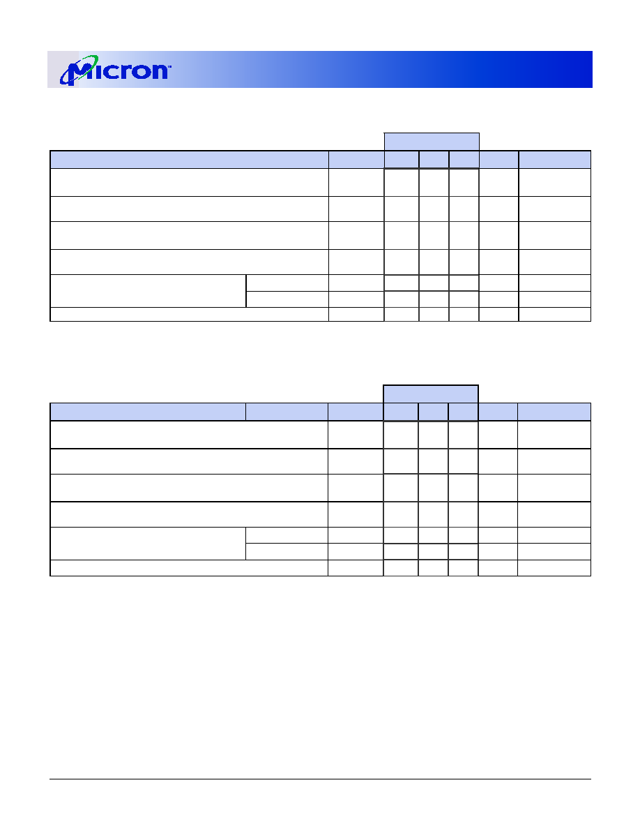
Table 10: DC Electrical Characteristics and Operating Conditions - 512MB Module
Notes: 1, 5, 6; notes appear on page 17; V
DD
= V
DD
Q = +3.3V ±0.3V
PARAMETER/CONDITION
SYMBOL
MIN
MAX
UNITS
NOTES
SUPPLY VOLTAGE
V
DD
, V
DD
Q
3
3.6
V
INPUT HIGH VOLTAGE: Logic 1; All inputs
V
IH
2
V
DD
+ 0.3
V
22
INPUT LOW VOLTAGE: Logic 0; All inputs
V
IL
-0.3
0.8
V
22
INPUT LEAKAGE CURRENT:
Any input 0V
£ VIN £ V
DD
(All other pins not under test = 0V)
Command and
Address Inputs,
CKE
I
I
-45
45
µA
33
CK0, S0#
-25
25
µA
CK2, S2#
-20
20
µA
DQMB
-5
5
µA
OUTPUT LEAKAGE CURRENT: DQ pins are
disabled; 0V
£ V
OUT
£ V
DD
Q
DQ
I
OZ
-5
5
µA
33
OUTPUT LEVELS:
Output High Voltage (I
OUT
= -4mA)
Output Low Voltage (I
OUT
= 4mA)
V
OH
2.4
≠
V
V
OL
≠
0.4
V
Table 11: DC Electrical Characteristics and Operating Conditions - 1GB Module
Notes: 1, 5, 6; notes appear on page 17; V
DD
= V
DD
Q = +3.3V ±0.3V
PARAMETER/CONDITION
SYMBOL
MIN
MAX
UNITS
NOTES
SUPPLY VOLTAGE
V
DD
, V
DD
Q
3
3.6
V
INPUT HIGH VOLTAGE: Logic 1; All inputs
V
IH
2
V
DD
+ 0.3
V
22
INPUT LOW VOLTAGE: Logic 0; All inputs
V
IL
-0.3
0.8
V
22
INPUT LEAKAGE CURRENT:
Any input 0V
£ VIN £ V
DD
(All other pins not under test = 0V)
Command and
Address Inputs
I
I
-90
90
µA
33
CKE
-45
45
µA
CK0, CK1, S0#, S1#
-25
25
µA
CK2, CK3, S2#, S3#
-20
20
µA
DQMB
-10
10
µA
OUTPUT LEAKAGE CURRENT: DQ pins are
disabled; 0V
£ V
OUT
£ V
DD
Q
DQ
I
OZ
-10
10
µA
33
OUTPUT LEVELS:
Output High Voltage (I
OUT
= -4mA)
Output Low Voltage (I
OUT
= 4mA)
V
OH
2.4
≠
V
V
OL
≠
0.4
V
512MB / 1GB (x72)
168-PIN SDRAM DIMM
ADVANCE
64, 128 Meg x72 SDRAM DIMM
Micron Technology, Inc., reserves the right to change products or specifications without notice.
SD9_18C64_128X72AG_A.fm - Rev. A 11/02 EN
13
©2002, Micron Technology Inc.
Table 12: I
DD
Specifications and Conditions ≠ 512MB Module
Notes: 1, 5, 6, 11, 13; notes appear on page 17; V
DD
= V
DD
Q = +3.3v ±0.3v; SDRAM component values only
MAX
PARAMETER/CONDITION
SYMBOL
-13E
-133 -10E
UNITS
NOTES
OPERATING CURRENT: Active Mode; Burst = 2; READ or
WRITE;
t
RC =
t
RC (MIN)
I
DD
1
1,935 1,800 1,800
mA
3, 18, 19, 30
STANDBY CURRENT: Power-Down Mode; All device device
banks idle; CKE = LOW
I
DD
2
18
18
18
mA
30
STANDBY CURRENT: Active Mode;CKE = HIGH; CS# = HIGH; All
device banks active after
t
RCD met; No accesses in progress
I
DD
3
720
720
720
mA
3, 12, 19, 30
OPERATING CURRENT: Burst Mode; Continuous burst; READ or
WRITE; All device banks active
I
DD
4
1,620 1,620 1,620
mA
3, 18, 19, 30
AUTO REFRESH CURRENT
t
RFC =
t
RFC (MIN)
I
DD
5
3,600 3,330 3,330
mA
3, 12
CKE = HIGH; CS# = HIGH
t
RFC = 7.8125µs
I
DD
6
90
90
90
mA
18, 19, 30, 31
SELF REFRESH CURRENT: CKE
£ 0.2V
I
DD
7
54
54
54
mA
4
Table 13: I
DD
Specifications and Conditions ≠ 1GB Module
Notes: 1, 5, 6, 11, 13; notes appear on page 17; V
DD
, V
DD
Q = +3.3V ±0.3V; SDRAM component values only
MAX
PARAMETER/CONDITION
SYMBOL
-13E
-133 -10E
UNITS
NOTES
OPERATING CURRENT: Active Mode; Burst = 2; READ or
WRITE;
t
RC =
t
RC (MIN)
I
DD
1
a
1,953 1,818 1,818
mA
3, 18, 19, 30
STANDBY CURRENT: Power-Down Mode; All device device
banks idle; CKE = LOW
I
DD
2
b
36
36
36
mA
30
STANDBY CURRENT: Active Mode; CKE = HIGH; CS# = HIGH;
All device banks active after
t
RCD met; No accesses in progress
I
DD
3
a
738
738
738
mA
3, 12, 19, 30
OPERATING CURRENT: Burst Mode; Continuous burst; READ
or WRITE; All device banks active
I
DD
4
a
1,638 1,638 1,638
mA
3, 18, 19, 30
AUTO REFRESH CURRENT
t
RFC =
t
RFC (MIN)
I
DD
5
b
7,200 6,660 6,660
mA
3, 12
CKE = HIGH; CS# = HIGH
t
RFC = 7.8125µs
I
DD
6
b
180
180
180
mA
18, 19, 30, 31
SELF REFRESH CURRENT: CKE
£ 0.2V
I
DD
7
b
108
108
108
mA
4
NOTE:
a - Value calculated as one module bank in this condition, and all other module banks in Power-Down Mode (I
DD2
).
b - Value calculated reflects all module banks in this condition.
512MB / 1GB (x72)
168-PIN SDRAM DIMM
ADVANCE
64, 128 Meg x72 SDRAM DIMM
Micron Technology, Inc., reserves the right to change products or specifications without notice.
SD9_18C64_128X72AG_A.fm - Rev. A 11/02 EN
14
©2002, Micron Technology Inc.
.
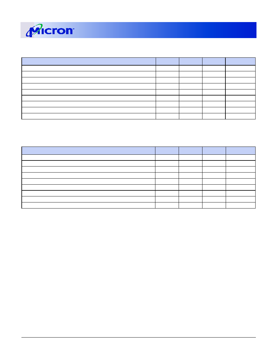
Table 14: Capacitance ≠ 512MB Module
Note 2; notes appear on page 17
PARAMETER
SYMBOL
MIN
MAX
UNITS
Input Capacitance: A0-A12, BA0, BA1, RAS#, CAS#, WE#
C
I
1
20
30.4
pF
Input Capacitance: CK0
C
I
2
12.5
17.5
pF
Input Capacitance: CK2
C
I
3
13.3
17.3
pF
Input Capacitance: S0#
C
I
4
12.5
19
pF
Input Capacitance: S2#
C
I
5
10
15.2
pF
Input Capacitance: CKE
C
I
6
20
30.4
pF
Input Capacitance: DQMB
C
I
7
2.5
3.8
pF
Input/Output Capacitance: SCL, SA, SDA
C
IO
1
≠
10
pF
Input/Output Capacitance: DQ
C
IO
2
4
6
pF
Table 15: Capacitance ≠ 1GB Module
Note 2; notes appear on page 17
PARAMETER
SYMBOL
MIN
MAX
UNITS
Input Capacitance: A0-A12, BA0, BA1, RAS#, CAS#, WE#
C
I
1
40
60.8
pF
Input Capacitance: CK0, CK1
C
I
2
12.5
17.5
pF
Input Capacitance: CK2, CK3
C
I
3
13.3
17.3
pF
Input Capacitance: S0#, S1#
C
I
4
12.5
19
pF
Input Capacitance: S2#, S3#
C
I
5
10
15.2
pF
Input Capacitance: CKE
C
I
6
20
30.4
pF
Input Capacitance: DQMB
C
I
7
5
7.6
pF
Input/Output Capacitance: SCL, SA, SDA
C
IO
1
≠
10
pF
Input/Output Capacitance: DQ
C
IO
2
8
12
pF
512MB / 1GB (x72)
168-PIN SDRAM DIMM
ADVANCE
64, 128 Meg x72 SDRAM DIMM
Micron Technology, Inc., reserves the right to change products or specifications without notice.
SD9_18C64_128X72AG_A.fm - Rev. A 11/02 EN
15
©2002, Micron Technology Inc.
.
Table 16: Electrical Characteristics and Recommended AC Operating Conditions
Notes: 5, 6, 8, 9, 11; notes appear on page 17
Module AC timing parameters comply with PC100 and PC133 Design Specs, based on component parameters
ACCHARACTERISTICS
-13E
-133
-10E
PARAMETER
SYMBOL
MIN
MAX
MIN
MAX
MIN
MAX
UNITS
NOTES
Access timefrom CLK (pos.edge)
CL=3
t
AC(3)
5.4
5.4
6
ns
27
CL=2
t
AC(2)
5.4
6
6
ns
Address hold time
t
AH
0.8
0.8
1
ns
Address setup time
t
AS
1.5
1.5
2
ns
CLK high-level width
t
CH
2.5
2.5
3
ns
CLK low-level width
t
CL
2.5
2.5
3
ns
Clock cycle time
CL=3
t
CK(3)
7
7.5
8
ns
23
CL = 2
t
CK(2)
7.5
10
10
ns
23
CKE holdt ime
t
CKH
0.8
0.8
1
ns
CKE setup time
t
CKS
1.5
1.5
2
ns
CS#, RAS#, CAS#, WE#, DQM hold time
t
CMH
0.8
0.8
1
ns
CS#, RAS#, CAS#, WE#, DQM setup time
t
CMS
1.5
1.5
2
ns
Data-in hold time
t
DH
0.8
0.8
1
ns
Data-in setup time
t
DS
1.5
1.5
2
ns
Data-out high-impedance time
CL = 3
t
HZ(3)
5.4
5.4
6
ns
10
CL = 2
t
HZ(2)
5.4
6
7
ns
10
Data-out low-impedance time
t
LZ
1
1
1
ns
Data-out hold time (load)
t
OH
3
3
3
ns
Data-out hold time (noload)
t
OH
N
1.8
1.8
1.8
ns
28
ACTIVE to PRECHARGE command
t
RAS
37
120,000
44
120,000
50
120,000
ns
29
ACTIVE to ACTIVE command period
t
RC
60
66
70
ns
ACTIVE to READ or WRITE delay
t
RCD
15
20
20
ns
Refresh period (8,192rows)
t
REF
64
64
64
ms
AUTOREFRESH period
t
RFC
66
66
70
ns
PRECHARGE command period
t
RP
15
20
20
ns
ACTIVE bank a to ACTIVE bank b
command
t
RRD
14
15
20
ns
Transition time
t
T
0.3
1.2
0.3
1.2
0.3
1.2
ns
7
WRITE recovery time
t
WR
1 CLK
+
1 CLK
+
1 CLK
+
ns
24
7ns
7.5ns
7ns
14
15
15
ns
25
Exit SELFREFRESH to ACTIVE command
t
XSR
67
75
80
ns
20
512MB / 1GB (x72)
168-PIN SDRAM DIMM
ADVANCE
64, 128 Meg x72 SDRAM DIMM
Micron Technology, Inc., reserves the right to change products or specifications without notice.
SD9_18C64_128X72AG_A.fm - Rev. A 11/02 EN
16
©2002, Micron Technology Inc.
Table 17: AC Functional Characteristics
Notes: 5, 6, 7, 8, 9, 11; notes appear on page 17
PARAMETER
SYMBOL
-13E
-133
-10E
UNITS
NOTES
READ/WRITE command to READ/WRITE command
t
CCD
1
1
1
t
CK
17
CKE to clock disable or power-down entry mode
t
CKED
1
1
1
t
CK
14
CKE to clock enable or power-down exit setup mode
t
PED
1
1
1
t
CK
14
DQM to input data delay
t
DQD
0
0
0
t
CK
17
DQM to data mask during WRITEs
t
DQM
0
0
0
t
CK
17
DQM to data high-impedance during READs
t
DQZ
2
2
2
t
CK
17
WRITE command to input data delay
t
DWD
0
0
0
t
CK
17
Data-in to ACTIVE command
t
DAL
4
5
4
t
CK
15, 21
Data-in to PRECHARGE command
t
DPL
2
2
2
t
CK
16, 21
Last data-in to burst STOP command
t
BDL
1
1
1
t
CK
17
Last data-in to new READ/WRITE command
t
CDL
1
1
1
t
CK
17
Last data-in to PRECHARGE command
t
RDL
2
2
2
t
CK
16, 21
LOAD MODE REGISTER command to ACTIVE or REFRESH command
t
MRD
2
2
2
t
CK
26
Data-out to high-impedance from PRECHARGE
command
CL = 3
t
ROH(3)
3
3
3
t
CK
17
CL = 2
t
ROH(2)
2
2
2
t
CK
17

512MB / 1GB (x72)
168-PIN SDRAM DIMM
ADVANCE
64, 128 Meg x72 SDRAM DIMM
Micron Technology, Inc., reserves the right to change products or specifications without notice.
SD9_18C64_128X72AG_A.fm - Rev. A 11/02 EN
17
©2002, Micron Technology Inc.
Notes
1. All voltages referenced to V
SS
.
2. This parameter is sampled. V
DD
, V
DDQ
= +3.3V;
T
A
= 25∞C; pin under test biased at 1.4V; f = 1
MHz.
3. I
DD
is dependent on output loading and cycle
rates. Specified values are obtained with mini-
mum cycle time and the outputs open.
4. Enables on-chip refresh and address counters.
5. The minimum specifications are used only to
indicate cycle time at which proper operation
over the full temperature range is ensured.
6. An initial pause of 100µs is required after power-
up, followed by two AUTO REFRESH commands,
before proper device operation is ensured. (V
DD
and V
DD
Q must be powered up simultaneously.
V
SS
and V
SS
Q must be at same potential.) The two
AUTO REFRESH command wake-ups should be
repeated any time the
t
REF refresh requirement is
exceeded.
7. AC characteristics assume
t
T = 1ns.
8. In addition to meeting the transition rate specifi-
cation, the clock and CKE must transit between
V
IH
and V
IL
(or between V
IL
and V
IH
) in a mono-
tonic manner.
9. Outputs measured at 1.5V with equivalent load:
10.
t
HZ defines the time at which the output achieves
the open circuit condition; it is not a reference to
V
OH
or V
OL
. The last valid data element will meet
t
OH before going High-Z.
11. AC timing and I
DD
tests have V
IL
= 0V and V
IH
=
3V, with timing referenced to 1.5V crossover
point. If the input transition time is longer than
1ns, then the timing is referenced at V
IL
(MAX)
and V
IH
(MIN) and no longer at the ISV crossover
point.
12. Other input signals are allowed to transition no
more than once every two clocks and are other-
wise at valid V
IH
or V
IL
levels.
13. I
DD
specifications are tested after the device is
properly initialized.
14. Timing actually specified by
t
CKS; clock(s) speci-
fied as a reference only at minimum cycle rate.
15. Timing actually specified by
t
WR plus
t
RP; clock(s)
specified as a reference only at minimum cycle
rate.
16. Timing actually specified by
t
WR.
17. Required clocks are specified by JEDEC function-
ality and are not dependent on any timing param-
eter.
18. The I
DD
current will increase or decrease propor-
tionally according to the amount of frequency
alteration for the test condition.
19. Address transitions average one transition every
two clocks.
20. CLK must be toggled a minimum of two times
during this period.
21. Based on
t
CK = 10ns for -10E;
t
CK = 7.5ns for -133
and -13E.
22. V
IH
overshoot: V
IH
(MAX) = V
DD
Q + 2V for a pulse
width
£ 3ns, and the pulse width cannot be
greater than one third of the cycle rate. V
IL
under-
shoot: V
IL
(MIN) = -2V for a pulse width
£ 3ns.
23. The clock frequency must remain constant (stable
clock is defined as a signal cycling within timing
constraints specified for the clock pin) during
access or precharge states (READ, WRITE, includ-
ing
t
WR, and PRECHARGE commands). CKE may
be used to reduce the data rate.
24. Auto precharge mode only. The precharge timing
budget (
t
RP) begins 7ns for -13E; 7.5ns for -133;
and 7ns for -10E after the first clock delay, after
the last WRITE is executed. May not exceed limit
set for precharge mode.
25. Precharge mode only.
26. JEDEC and PC100 specify three clocks.
27.
t
AC for -133/-13E at CL = 3 with no load is 4.6ns
and is guaranteed by design.
28. Parameter guaranteed by design.
29. For -13E, CL = 2 and
t
CK = 7.5ns; for -133, CL = 3
and
t
CK = 7.5ns; for -10E, CL=2 and
t
CK = 10ns
30. CKE is HIGH during refresh command period
t
RFC (MIN) else CKE is LOW. The I
DD
6 limit is
actually a nominal value and does not result in a
fail value.
31. Refer to device data sheet for timing waveforms.
32. The value of
t
RAS used in -13E speed grade mod-
ules is calculated from
t
RC -
t
RP.
33. Leakage number reflects the worst case leakage
possible through the module pin, not what each
memory device contributes.
Q
50pF
512MB / 1GB (x72)
168-PIN SDRAM DIMM
ADVANCE
64, 128 Meg x72 SDRAM DIMM
Micron Technology, Inc., reserves the right to change products or specifications without notice.
SD9_18C64_128X72AG_A.fm - Rev. A 11/02 EN
18
©2002, Micron Technology Inc.
SPD Clock and Data Conventions
Data states on the SDA line can change only during
SCL LOW. SDA state changes during SCL HIGH are
reserved for indicating start and stop conditions (as
shown in Figure 7 and Figure 8).
SPD Start Condition
All commands are preceded by the start condition,
which is a HIGH-to-LOW transition of SDA when SCL
is HIGH. The SPD device continuously monitors the
SDA and SCL lines for the start condition and will not
respond to any command until this condition has
been met.
SPD Stop Condition
All communications are terminated by a stop condi-
tion, which is a LOW-to-HIGH transition of SDA when
SCL is HIGH. The stop condition is also used to place
the SPD device into standby power mode.
SPD Acknowledge
Acknowledge is a software convention used to indi-
cate successful data transfers. The transmitting device,
either master or slave, will release the bus after trans-
mitting eight bits. During the ninth clock cycle, the
receiver will pull the SDA line LOW to acknowledge
that it received the eight bits of data (as shown in
Figure 9).
The SPD device will always respond with an
acknowledge after recognition of a start condition and
its slave address. If both the device and a WRITE oper-
ation have been selected, the SPD device will respond
with an acknowledge after the receipt of each subse-
quent eight bit word. In the read mode the SPD device
will transmit eight bits of data, release the SDA line
and monitor the line for an acknowledge. If an
acknowledge is detected and no stop condition is gen-
erated by the master, the slave will continue to trans-
mit data. If an acknowledge is not detected, the slave
will terminate further data transmissions and await
the stop condition to return to standby power mode.
Figure 7: Data Validity
Figure 8: Definition of Start and Stop
Figure 9: Acknowledge Response From Receiver
SCL
SDA
DATA STABLE
DATA STABLE
DATA
CHANGE
SCL
SDA
START
BIT
STOP
BIT
SCL from Master
Data Output
from Transmitter
Data Output
from Receiver
9
8
Acknowledge
512MB / 1GB (x72)
168-PIN SDRAM DIMM
ADVANCE
64, 128 Meg x72 SDRAM DIMM
Micron Technology, Inc., reserves the right to change products or specifications without notice.
SD9_18C64_128X72AG_A.fm - Rev. A 11/02 EN
19
©2002, Micron Technology Inc.
Table 18: EEPROM Device Select Code
The most significant bit (b7) is sent first
DEVICE TYPE IDENTIFIER
CHIP ENABLE
RW
b7
b6
b5
b4
b3
b2
b1
b0
Memory Area Select Code (two arrays)
1
0
1
0
SA2
SA1
SA0
RW
Protection Register Select Code
0
1
1
0
SA2
SA1
SA0
RW
Table 19: EEPROM Operating Modes
MODE
RW BIT
WC
BYTES
INITIAL SEQUENCE
Current Address Read
1
VIH or VIL
1
Start, Device Select, RW = 1
RandomAddressRead
0
VIH or VIL
1
Start, Device Select, RW= 0, Address
1
VIH or VIL
RESTART, Device Select, RW= 1
Sequential Read
1
VIH or VIL
≥ 1
Similar to Current or Random Address Read
Byte Write
0
V
IL
1
START, Device Select, RW = 0
Page Write
0
V
IL
£ 16
START, Device Select, RW = 0
Table 20: Serial Presence-Detect EEPROM DC Operating Conditions
V
DD
= +3.3V ±0.3V; all voltages referenced to V
SS
PARAMETER/CONDITION
SYMBOL
MIN
MAX
UNITS
SUPPLY VOLTAGE
V
DD
3
3.6
V
INPUT HIGH VOLTAGE: Logic 1; All inputs
V
IH
V
DD
x 0.7
V
DD
+ 0.5
V
INPUT LOW VOLTAGE: Logic 0; All inputs
V
IL
-1
V
DD
x 0.3
V
OUTPUT LOW VOLTAGE: I
OUT
= 3mA
V
OL
≠
0.4
V
INPUT LEAKAGE CURRENT: V
IN
= GND to V
DD
I
LI
-10
10
µA
OUTPUT LEAKAGE CURRENT: V
OUT
= GND to V
DD
I
LO
-10
10
µA
STANDBY CURRENT: SCL = SDA = V
DD
- 0.3V; All other
inputs = GND or 3.3V ±10%
I
CCS
≠
30
µA
POWER SUPPLY CURRENT:
I
CC
Write
I
CC
Read
≠
≠
3
1
mA
512MB / 1GB (x72)
168-PIN SDRAM DIMM
ADVANCE
64, 128 Meg x72 SDRAM DIMM
Micron Technology, Inc., reserves the right to change products or specifications without notice.
SD9_18C64_128X72AG_A.fm - Rev. A 11/02 EN
20
©2002, Micron Technology Inc.
Figure 10: SPD EEPROM Timing Diagram
NOTE:
1. The SPD EEPROM WRITE cycle time (
t
WRC) is the time from a valid stop condition of a write sequence to the end of
the EEPROM internal erase/program cycle. During the WRITE cycle, the EEPROM bus interface circuit is disabled, SDA
remains HIGH due to pull-up resistor, and the EEPROM does not respond to its slave address.
SCL
SDA IN
SDA OUT
tLOW
tSU:STA
tHD:STA
tF
tHIGH
tR
tBUF
tDH
tAA
tSU:STO
tSU:DAT
tHD:DAT
UNDEFINED
Table 21: Serial Presence-Detect EEPROM AC Operating Conditions
V
DD
= +3.3V ±0.3V; all voltages referenced to V
SS
PARAMETER/CONDITION
SYMBOL
MIN
MAX
UNITS
NOTES
SCL LOW to SDA data-out valid
t
AA
≠
3.5
µs
Time the bus must be free before a new transition can
start
t
BUF
4.7
≠
µs
Data-out hold time
t
DH
300
ns
SDA and SCL fall time
t
F
300
ns
Data-in hold time
t
HD:DAT
0
µs
Start condition hold time
t
HD:STA
4
µs
ClockHIGHperiod
t
HIGH
4
µs
Noise suppression time constant at SCL, SDA inputs
t
I
100
ns
Clock LOW period
t
LOW
4.7
µs
SDA and SCL rise time
t
R
1
µs
SCL clock frequency
f
SCL
100
KHz
Data-in setup time
t
SU:DAT
250
ns
Start condition setup time
t
SU:STA
4.7
µs
Stop condition setup time
t
SU:STO
4.7
µs
WRITE cycle time
t
WRC
10
ms
1
512MB / 1GB (x72)
168-PIN SDRAM DIMM
ADVANCE
64, 128 Meg x72 SDRAM DIMM
Micron Technology, Inc., reserves the right to change products or specifications without notice.
SD9_18C64_128X72AG_A.fm - Rev. A 11/02 EN
21
©2002, Micron Technology Inc.
Table 22: Seriea Presence-Detect Matrix
V
DD
= +3.3V ±0.3V; "1"/"0": Serial Data, "driven to HIGH"/"driven to LOW"
BYTE
DESCRIPTION
ENTRY
(VERSION)
MT9LSDT6472A
MT18LSDT12872A
0
NUMBER OF BYTES USED BY MICRON
128
80
80
1
TOTAL NUMBER OF SPD MEMORY BYTES
256
08
08
2
MEMORY TYPE
SDRAM
04
04
3
NUMBER OF ROW ADDRESSES
12
0D
0D
4
NUMBER OF COLUMN ADDRESSES
10
0A
0A
5
NUMBER OF MODULE BANKS
1 or 2
01
02
6
MODULE DATA WIDTH
72
48
48
7
MODULE DATA WIDTH (continued)
0
00
00
8
MODULE VOLTAGE INTERFACE LEVELS
LVTTL
01
01
9
SDRAM CYCLE TIME,
t
CK
(CAS LATENCY = 3)
7ns (-13E)
70
75
80
75
75
80
10
SDRAM ACCESS FROM CLK,
t
AC
(CAS LATENCY = 3)
5.4ns (-13E/-133)
6ns (-10E)
54
60
54
60
11
MODULE CONFIGURATION TYPE
ECC
02
02
12
REFRESH RATE/TYPE
7.8125µs/SELF
82
82
13
SDRAM WIDTH (PRIMARY SDRAM)
8
08
08
14
ERROR-CHECKING SDRAM DATA WIDTH
8
08
08
15
MINIMUM CLOCK DELAY FROM BACK-TO-BACK
RANDOM COLUMN ADDRESSES,
t
CCD
1
01
01
16
BURST LENGTHS SUPPORTED
1, 2, 4, 8, PAGE
8F
8F
17
NUMBER OF BANKS ON SDRAM DEVICE
4
04
04
18
CAS LATENCIES SUPPORTED
2, 3
06
06
19
CS LATENCY
0
01
01
20
WE LATENCY
0
01
01
21
SDRAM MODULE ATTRIBUTES
UNBUFFERED
00
00
22
SDRAM DEVICE ATTRIBUTES:GENERAL
0E
0E
0E
23
SDRAM CYCLE TIME ,
t
CK
(CAS LATENCY = 2) 10 (-133/-10E) A0
7.5ns (13E)
10ns (-133/-10E)
75
A0
75
A0
24
SDRAM ACCESS FROM CLK,
t
AC
(CAS LATENCY = 2)
5.4ns (-13E)
6ns (-133/-10E)
54
60
54
60
25
SDRAM CYCLE TIME,
t
CK (CAS LATENCY = 1)
00
00
26
SDRAM ACCESS FROM CLK,
t
AC (CAS LATENCY = 1)
00
00
27
MINIMUM ROW PRECHARGE TIME,
t
RP
15ns (-13E)
20ns (-133/-10E)
0F
14
0F
14
28
MINIMUM ROW ACTIVE TO ROW ACTIVE,
t
RRD
14ns (-13E)
15ns (-133)
20ns (-10E)
0E
0F
14
0E
0F
14
29
MINIMUM RAS# TO CAS# DELAY,
t
RCD
15ns (-13E)
20ns (-133/-10E)
0F
14
0F
14
30
MINIMUM RAS# PULSE WIDTH,
t
RAS (See note 1)
45ns (-13E)
44ns (133)
50ns (-10E)
2D
2C
32
2D
2C
32
31
MODULE BANK DENSITY
512MB
80
80
512MB / 1GB (x72)
168-PIN SDRAM DIMM
ADVANCE
64, 128 Meg x72 SDRAM DIMM
Micron Technology, Inc., reserves the right to change products or specifications without notice.
SD9_18C64_128X72AG_A.fm - Rev. A 11/02 EN
22
©2002, Micron Technology Inc.
NOTE:
1. The value of
t
RAS used for -13E modules is calculated from
t
RC -
t
RP. Actual device specification value is 37ns.
32
COMMAND AND ADDRESS SETUP TIME,
t
AS,
t
CMS 1.5ns (-13E/-133)
2ns (-10E)
15
20
15
20
33
COMMAND AND ADDRESS HOLD TIME,
t
AH,
t
CMH 0.8ns (-13E/-133)
1ns (-10E)
08
10
08
10
34
DATA SIGNAL INPUT SETUP TIME,
t
DS
1.5ns (-13E/-133)
2ns (-10E)
15
20
15
20
35
DATA SIGNAL INPUT HOLD TIME,
t
DH
0.8ns (-13E/-133
1ns (-10E))
08
10
08
10
36-61
RESERVED
00
00
62
SPD REVISION
REV. 1.2
12
12
63
CHECKSUM FOR BYTES 0-62
(-13E)
(-133)
(-10E)
DE
24
6C
DF
25
6D
64
MANUFACTURER'S JEDEC ID CODE
MICRON
2C
2C
65-71
MANUFACTURER'S JEDEC ID CODE(CONT.)
FF
FF
72
MANUFACTURING LOCATION
1 - 11
01 - 0B
01 - 0B
73-90
MODULE PARTNUMBER (ASCII)
Variable Data
Variable Data
91
PCB IDENTIFICATION CODE
1 - 9
01-09
01-09
92
IDENTIFICATION CODE (CONT.)
0
00
00
93
YEAR OF MANUFACTURE IN BCD
Variable Data
Variable Data
94
WEEK OF MANUFACTURE IN BCD
Variable Data
Variable Data
95-98
MODULE SERIAL NUMBER
Variable Data
Variable Data
99-125
MANUFACTURER-SPECIFIC DATA (RSVD)
126
SYSTEM FREQUENCY
100 MHz (-13E/
-133/-10E)
64
64
127
SDRAM COMPONENT & CLOCK DETAIL
AF
FF
Table 22: Seriea Presence-Detect Matrix (Continued)
V
DD
= +3.3V ±0.3V; "1"/"0": Serial Data, "driven to HIGH"/"driven to LOW"
BYTE
DESCRIPTION
ENTRY
(VERSION)
MT9LSDT6472A
MT18LSDT12872A
512MB / 1GB (x72)
168-PIN SDRAM DIMM
ADVANCE
64, 128 Meg x72 SDRAM DIMM
Micron Technology, Inc., reserves the right to change products or specifications without notice.
SD9_18C64_128X72AG_A.fm - Rev. A 11/02 EN
23
©2002, Micron Technology Inc.
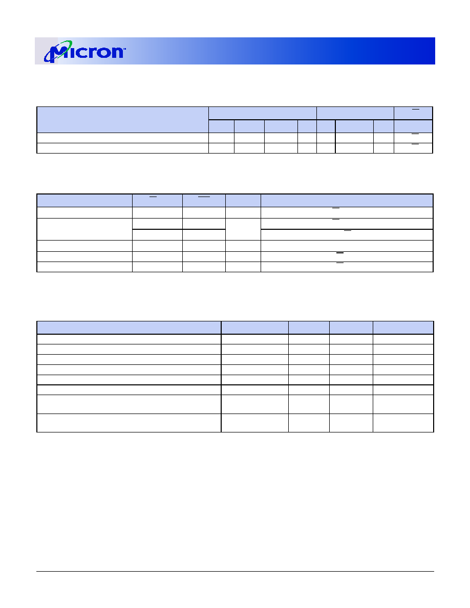
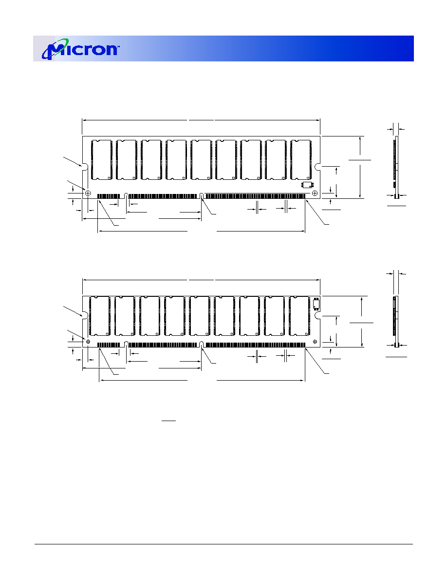
Figure 11: 512MB Module Dimensions
NOTE:
All dimensions in inches (millimeters)
or typical where noted.
.125 (3.18)
MAX
.054 (1.37)
.046 (1.17)
PIN 1 (PIN 85 ON BACKSIDE)
.700 (17.78)
TYP
.118 (3.00)
(2X)
.118 (3.00) TYP
4.550 (115.57)
.050 (1.27)
TYP
.118 (3.00)
TYP
.039 (1.00)
TYP
.079 (2.00) R
(2X)
.039 (1.00)R (2X)
FRONT VIEW
.128 (3.25)
.118 (3.00)
PIN 84 (PIN 168 ON BACKSIDE)
(2X)
.250 (6.35) TYP
1.661 (42.18)
2.625 (66.68)
1.380 (35.05)
1.370 (34.80)
5.256 (133.50)
5.244 (133.20)
U1
U2
U3
U4
U5
U6
U7
U8
U9
U10
STANDARD PCB
.125 (3.18)
MAX
.054 (1.37)
.046 (1.17)
PIN 1 (PIN 85 ON BACKSIDE)
.700 (17.78)
TYP
.118 (3.00)
(2X)
.118 (3.00) TYP
4.550 (115.57)
.050 (1.27)
TYP
.118 (3.00)
TYP
.039 (1.00)
TYP
.079 (2.00) R
(2X)
.039 (1.00)R (2X)
FRONT VIEW
.128 (3.25)
.118 (3.00)
PIN 84 (PIN 168 ON BACKSIDE)
(2X)
.250 (6.35) TYP
1.661 (42.18)
2.625 (66.68)
1.131 (28.73)
1.119 (28.42)
5.256 (133.50)
5.244 (133.20)
U1
U2
U3
U4
U5
U6
U7
U8
U9
U10
LOW PROFILE PCB
MAX
MIN
Æ
8000 S. Federal Way, P.O. Box 6, Boise, ID 83707-0006, Tel: 208-368-3900
E-mail: prodmktg@micron.com, Internet: http://www.micron.com, Customer Comment Line: 800-932-4992
Micron, the M logo, and the Micron logo are trademarks and/or service marks of Micron Technology, Inc.
512MB / 1GB (x72)
168-PIN SDRAM DIMM
ADVANCE
64, 128 Meg x72 SDRAM DIMM
©2002, Micron Technology Inc.
SD9_18C64_128X72AG_A.fm - Rev. A 11/02 EN
24
Figure 12: 1GB Module Dimensions
NOTE:
All dimensions in inches (millimeters)
or typical where noted.
Data Sheet Designation
Advance: This data sheet contains initial descrip-
tions of products still under deveopment.
.157 (3.99)
MAX
.054 (1.37)
.046 (1.17)
PIN 1
.700 (17.78)
TYP
.118 (3.00)
(2X)
.118 (3.00) TYP
4.550 (115.57)
.050 (1.27)
TYP
.118 (3.00)
TYP
.039 (1.00)
TYP
.079 (2.00) R
(2X)
.039 (1.00)R (2X)
FRONT VIEW
.128 (3.25)
.118 (3.00)
PIN 84
(2X)
.250 (6.35) TYP
1.661 (42.18)
2.625 (66.68)
1.131 (28.73)
1.119 (28.42)
5.256 (133.50)
5.244 (133.20)
U1
U2
U3
U4
U5
U6
U7
U8
U9
U10
LOW PROFILE PCB
U11
U12
U13
U14
U15
U16
U17
U18
U19
PIN 85
PIN 168
BACK VIEW
.157 (3.99)
MAX
.054 (1.37)
.046 (1.17)
PIN 1
.700 (17.78)
TYP
.118 (3.00)
(2X)
.118 (3.00) TYP
4.550 (115.57)
.050 (1.27)
TYP
.118 (3.00)
TYP
.039 (1.00)
TYP
.079 (2.00) R
(2X)
.039 (1.00)R (2X)
FRONT VIEW
.128 (3.25)
.118 (3.00)
PIN 84
(2X)
.250 (6.35) TYP
1.661 (42.18)
2.625 (66.68)
1.380 (35.05)
1.370 (34.80)
5.256 (133.50)
5.244 (133.20)
U1
U2
U3
U4
U5
U6
U7
U8
U9
U10
STANDARD PCB
U11
U12
U13
U14
U15
U16
U17
U18
U19
PIN 85
PIN 168
BACK VIEW
MAX
MIN