PRODUCTS AND SPECIFICATIONS DISCUSSED HEREIN ARE SUBJECT TO CHANGE BY MICRON WITHOUT NOTICE.
09005aef808ffdc7
DD9_18C16_32_64_128X72PHG_E.fm - Rev. E 7/03 EN
1
�2003 Micron Technology, Inc. All rights reserved.
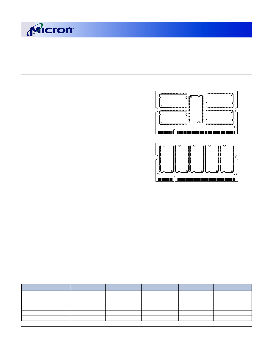
128MB, 256MB, 512MB, 1GB (x72, ECC, PLL)
200-PIN DDR SDRAM SODIMM
DDR SDRAM
SMALL-OUTLINE DIMM
MT9VDDT1672PH(I) � 128MB, MT9VDDT3272PH(I) �
256MB, MT18VDDT6472PH(I) � 512MB,
MT9VDDT6472PH(I) � 512MB,
MT18VDDT12872PH(I) � 1GB
For the lastest data sheet, please refer to the Micron
�
Web site:
www.micron.com/moduleds.
Features
� 200-pin, small-outline, dual in-line memory
module (SODIMM)
� ECC, 1-bit error detection and correction
� Fast data transfer rates: PC1600, PC2100, and
PC2700
� Utilizes 200 MT/s, 266 MT/s, and 333 MT/s DDR
SDRAM components
� MT9VDDT1672PH (16 Meg x 72); MT9VDDT3272PH (32 Meg
x 72); MT18VDDT6472PH (64 Meg x 72); MT9VDDT6472PH
(32 Meg x 72, stacked); MT18VDDT12872PH (64 Meg x 72,
stacked)
� V
DD
= V
DD
Q = +2.5V
� V
DDSPD
= +2.3V to +3.6V
� 2.5V I/O (SSTL_2 compatible)
� Commands entered on each positive CK edge
� DQS edge-aligned with data for READs; center-
aligned with data for WRITEs
NOTE:
1. CL = Device CAS (READ) Latency.
2. -335 and -262 speed grades available in single-
rank module only.
3. Consult Micron for availability; industrial tem-
perature option available in -265 speed only.
Figure 1: 200-Pin SODIMM (MO-224)
� Internal, pipelined double data rate (DDR)
architecture; two data accesses per clock cycle
� Four internal device banks for concurrent operation
� Programmable burst lengths: 2, 4, or 8
� Auto precharge option
� Auto Refresh and Self Refresh Modes
� 15.625�s (MT9VDDT1672PH), 7.8125�s
(MT9VDDT3272PH, MT18VDDT6472PH,
MT9VDDT6472PH, MT18VDDT12872PH)
maximum average periodic refresh interval
� Serial Presence Detect (SPD) with EEPROM
� Programmable READ CAS latency
� Gold edge contacts
� Bidirectional data strobe (DQS) transmitted/re-
ceived with data--i.e., source-synchronous data
capture
� Differential clock inputs CK and CK#
OPTIONS
MARKING
� Operating Temperature Range
Commercial (0�C
� T
A
� +70�C)
None
Industrial (-40�C
� T
A
� +85�C)
I
3
� Package
200-pin SODIMM (standard)
G
200-pin SODIMM (lead-free)
Y
� Clock Frequency/CAS Latency
6ns, 267 MHz (333 MT/s) / CL = 2.5
1
-335
2
7.5ns, 133 MHz (266 MT/s)/ CL = 2
-262
7.5ns, 133 MHz (266 MT/s)/ CL = 2
-26A
7.5ns, 133 MHz (266 MT/s)/ CL = 2.5
-265
10ns, 100 MHz (200 MT/s)/ CL = 2
-202
� PCB
Standard: 1.5in. (38.10mm)
Low-Profile: 1.25in. (31.75mm)
Standard: 1.50in. (38.10mm)
Low Profile: 1.25in. (31.75mm)
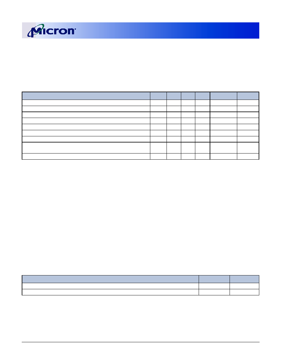
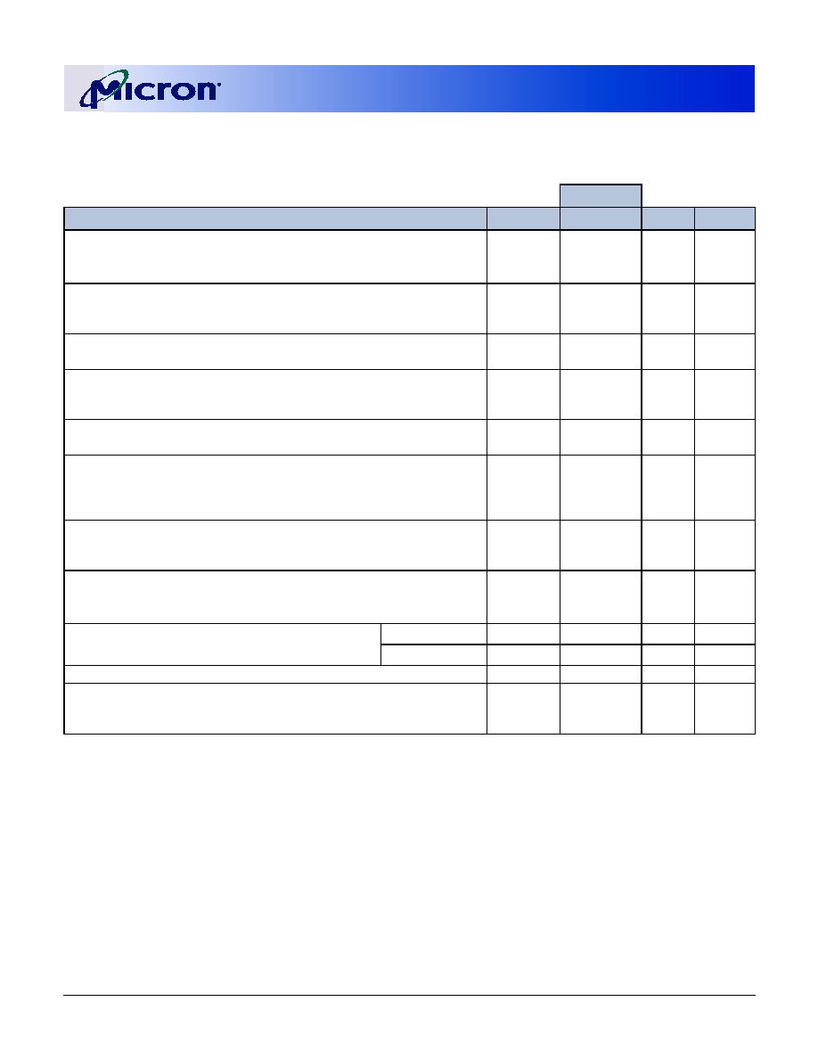
Table 1:
Address Table
MT9VDDT1672PH MT9VDDT3272PH
MT18VDDT6472PH MT9VDDT6472PH MT18VDDT12872PH
Refresh Count
4K
8K
8K
8K
8K
Row Addressing
4K (A0�A11)
8K (A0�A12)
8K (A0�A12)
8K (A0�A12)
8K (A0�A12)
DeviceBankAddressing
4 (BA0, BA1)
4 (BA0, BA1)
4 (BA0, BA1)
4 (BA0, BA1)
4 (BA0, BA1)
Base Device Configuration
16 Meg x 8
32 Meg x 8
32 Meg x 8
64 Meg x 8
64 Meg x 8
Column Addressing
1K (A0�A9)
1K (A0�A9)
1K (A0�A9)
2K (A0�A9, A11)
2K (A0�A9, A11)
Module Rank Addressing
1 (S0#)
1 (S0#)
2 (S0#, S1#)
1 (S0#)
2 (S0#, S1#)
128MB, 256MB, 512MB, 1GB (x72, ECC, PLL)
200-PIN DDR SDRAM SODIMM
09005aef808ffdc7
Micron Technology, Inc., reserves the right to change products or specifications without notice.
DD9_18C16_32_64_128X72PHG_E.fm - Rev. E 7/03 EN
2
�2003 Micron Technology, Inc. All rights reserved.
NOTE:
All part numbers end with a two-place code (not shown), designating component and PCB revisions. Consult factory for
current revision codes. Example: MT9VDDT3272PHG-265A1.
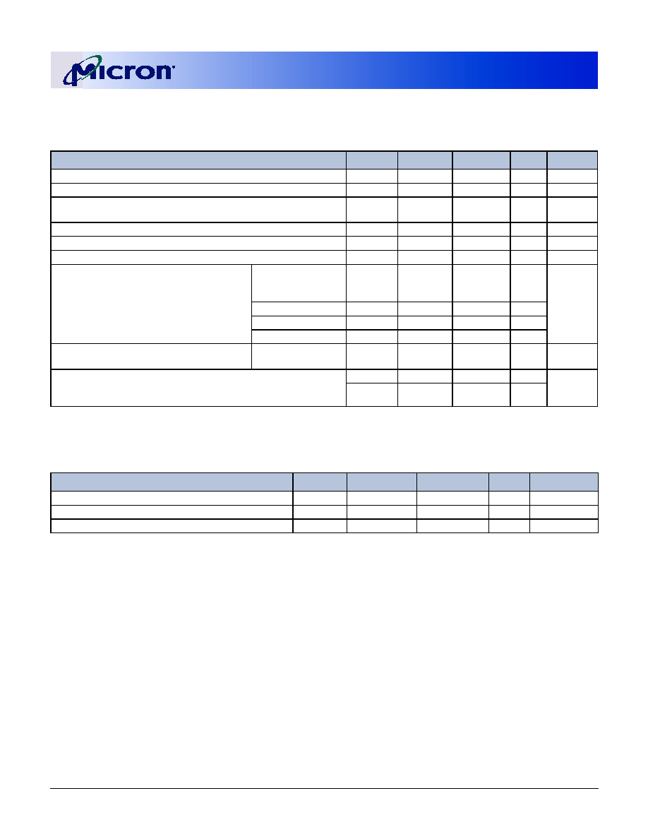
Table 2:
Part Numbers and Timing Parameters
PART NUMBER
MODULE
DENSITY
CONFIGURATION
MODULE
BANDWIDTH
MEMORY CLOCK/
DATA RATE
CLOCK LATENCY
(CL -
t
RCD -
t
RP)
MT9VDDT1672PHG-335_
128MB
16 Meg x 72
2.7 GB/s
6ns, 333 MT/s
2.5-3-3
MT9VDDT1672PHY-335_
128MB
16 Meg x 72
2.7 GB/s
6ns, 333 MT/s
2.5-3-3
MT9VDDT1672PHG-262_
128MB
16 Meg x 72
2.1 GB/s
7.5ns, 266 MT/s
2-2-2
MT9VDDT1672PHY-262_
128MB
16 Meg x 72
2.1 GB/s
7.5ns, 266 MT/s
2-2-2
MT9VDDT1672PHG-26A_
128MB
16 Meg x 72
2.1 GB/s
7.5ns, 266 MT/s
2-3-3
MT9VDDT1672PHY-26A_
128MB
16 Meg x 72
2.1 GB/s
7.5ns, 266 MT/s
2-3-3
MT9VDDT1672PH(I)G-265_
128MB
16 Meg x 72
2.1 GB/s
7.5ns, 266 MT/s
2.5-3-3
MT9VDDT1672PH(I)Y-265_
128MB
16 Meg x 72
2.1 GB/s
7.5ns, 266 MT/s
2.5-3-3
MT9VDDT1672PHG-202_
128MB
16 Meg x 72
1.6 GB/s
10ns, 200 MT/s
2-2-2
MT9VDDT1672PHY-202_
128MB
16 Meg x 72
1.6 GB/s
10ns, 200 MT/s
2-2-2
MT9VDDT3272PHG-335_
256MB
32 Meg x 72
2.7 GB/s
6ns, 333 MT/s
2.5-3-3
MT9VDDT3272PHY-335_
256MB
32 Meg x 72
2.7 GB/s
6ns, 333 MT/s
2.5-3-3
MT9VDDT3272PHG-262_
256MB
32 Meg x 72
2.1 GB/s
7.5ns, 266 MT/s
2-2-2
MT9VDDT3272PHY-262_
256MB
32 Meg x 72
2.1 GB/s
7.5ns, 266 MT/s
2-2-2
MT9VDDT3272PHG-26A_
256MB
32 Meg x 72
2.1 GB/s
7.5ns, 266 MT/s
2-3-3
MT9VDDT3272PHY-26A_
256MB
32 Meg x 72
2.1 GB/s
7.5ns, 266 MT/s
2-3-3
MT9VDDT3272PH(I)G-265_
256MB
32 Meg x 72
2.1 GB/s
7.5ns, 266 MT/s
2.5-3-3
MT9VDDT3272PH(I)Y-265_
256MB
32 Meg x 72
2.1 GB/s
7.5ns, 266 MT/s
2.5-3-3
MT9VDDT3272PHG-202_
256MB
32 Meg x 72
1.6 GB/s
10ns, 200 MT/s
2-2-2
MT9VDDT3272PHY-202_
256MB
32 Meg x 72
1.6 GB/s
10ns, 200 MT/s
2-2-2
MT18VDDT6472PHG-335_
512MB
64 Meg x 72
2.7 GB/s
6ns, 333 MT/s
2.5-3-3
MT18VDDT6472PHY-335_
512MB
64 Meg x 72
2.7 GB/s
6ns, 333 MT/s
2.5-3-3
MT18VDDT6472PHG-262_
512MB
64 Meg x 72
2.1 GB/s
7.5ns, 266 MT/s
2-2-2
MT18VDDT6472PHY-262_
512MB
64 Meg x 72
2.1 GB/s
7.5ns, 266 MT/s
2-2-2
MT18VDDT6472PHG-26A_
512MB
64 Meg x 72
2.1 GB/s
7.5ns, 266 MT/s
2-3-3
MT18VDDT6472PHY-26A_
512MB
64 Meg x 72
2.1 GB/s
7.5ns, 266 MT/s
2-3-3
MT18VDDT6472PH(I)G-265_
512MB
64 Meg x 72
2.1 GB/s
7.5ns, 266 MT/s
2.5-3-3
MT18VDDT6472PH(I)Y-265_
512MB
64 Meg x 72
2.1 GB/s
7.5ns, 266 MT/s
2.5-3-3
MT18VDDT6472PHG-202_
512MB
64 Meg x 72
1.6 GB/s
10ns, 200 MT/s
2-2-2
MT18VDDT6472PHY-202_
512MB
64 Meg x 72
1.6 GB/s
10ns, 200 MT/s
2-2-2
MT9VDDT6472PHG-335_
512MB
64 Meg x 72
2.7 GB/s
6ns, 333 MT/s
2.5-3-3
MT9VDDT6472PHY-335_
512MB
64 Meg x 72
2.7 GB/s
6ns, 333 MT/s
2.5-3-3
MT9VDDT6472PHG-262_
512MB
64 Meg x 72
2.1 GB/s
7.5ns, 266 MT/s
2-2-2
MT9VDDT6472PHY-262_
512MB
64 Meg x 72
2.1 GB/s
7.5ns, 266 MT/s
2-2-2
MT9VDDT6472PHG-26A_
512MB
64 Meg x 72
2.1 GB/s
7.5ns, 266 MT/s
2-3-3
MT9VDDT6472PHY-26A_
512MB
64 Meg x 72
2.1 GB/s
7.5ns, 266 MT/s
2-3-3
MT9VDDT6472PH(I)G-265_
512MB
64 Meg x 72
2.1 GB/s
7.5ns, 266 MT/s
2.5-3-3
MT9VDDT6472PH(I)Y-265_
512MB
64 Meg x 72
2.1 GB/s
7.5ns, 266 MT/s
2.5-3-3
MT9VDDT6472PHG-202_
512MB
64 Meg x 72
1.6 GB/s
10ns, 200 MT/s
2-2-2
MT9VDDT6472PHY-202_
512MB
64 Meg x 72
1.6 GB/s
10ns, 200 MT/s
2-2-2
MT18VDDT12872PHG-335_
1GB
128 Meg x 72
2.7 GB/s
6ns, 333 MT/s
2.5-3-3
MT18VDDT12872PHY-335_
1GB
128 Meg x 72
2.7 GB/s
6ns, 333 MT/s
2.5-3-3
MT18VDDT12872PHG-262_
1GB
128 Meg x 72
2.1 GB/s
7.5ns, 266 MT/s
2-2-2
MT18VDDT12872PHY-262_
1GB
128 Meg x 72
2.1 GB/s
7.5ns, 266 MT/s
2-2-2
MT18VDDT12872PHG-26A_
1GB
128 Meg x 72
2.1 GB/s
7.5ns, 266 MT/s
2-3-3
MT18VDDT12872PHY-26A_
1GB
128 Meg x 72
2.1 GB/s
7.5ns, 266 MT/s
2-3-3
MT18VDDT12872PH(I)G-265_
1GB
128 Meg x 72
2.1 GB/s
7.5ns, 266 MT/s
2.5-3-3
MT18VDDT12872PH(I)Y-265_
1GB
128 Meg x 72
2.1 GB/s
7.5ns, 266 MT/s
2.5-3-3
MT18VDDT12872PHG-202_
1GB
128 Meg x 72
1.6 GB/s
10ns, 200 MT/s
2-2-2
MT18VDDT12872PHY-202_
1GB
128 Meg x 72
1.6 GB/s
10ns, 200 MT/s
2-2-2
128MB, 256MB, 512MB, 1GB (x72, ECC, PLL)
200-PIN DDR SDRAM SODIMM
09005aef808ffdc7
Micron Technology, Inc., reserves the right to change products or specifications without notice.
DD9_18C16_32_64_128X72PHG_E.fm - Rev. E 7/03 EN
3
�2003 Micron Technology, Inc. All rights reserved.
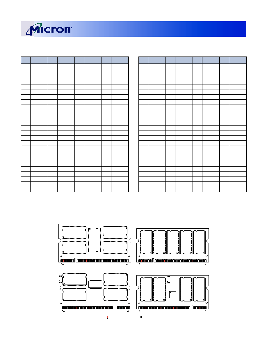
NOTE:
Pin 99 is a No Connect for MT9VDDT1672PH module, A12 for all other modules.
Figure 2: Module Layout
Table 3:
Pin Assignment
(200-Pin SODIMM Front)
PIN SYMBOL PIN SYMBOL PIN SYMBOL PIN SYMBOL
1
V
REF
51
V
SS
101
A9
151
DQ42
3
V
SS
53
DQ19
103
V
SS
153
DQ43
5
DQ0
55
DQ24
105
A7
155
V
DD
7
DQ1
57
V
DD
107
A5
157
V
DD
9
Vdd
59
DQ25
109
A3
159
V
SS
11
DQS0
61
DQS3
111
A1
161
V
SS
13
DQ2
63
V
SS
113
V
DD
163
DQ48
15
V
SS
65
DQ26
115 A10
/AP
165
DQ49
17
DQ3
67
DQ27
117
BA0
167
V
DD
19
DQ8
69
V
DD
119
WE#
169
DQS6
21
V
DD
71
CB0
121
S0#
171
DQ50
23
DQ9
73
CB1
123
NC
173
V
SS
25
DQS1
75
V
SS
125
V
SS
175
DQ51
27
V
SS
77
DQS8
127
DQ32
177
DQ56
29
DQ10
79
CB2
129
DQ33
179
V
DD
31
DQ11
81
V
DD
131
V
DD
181
DQ57
33
V
DD
83
CB3
133
DQS4
183
DQS7
35
CK0
85
NC
135
DQ34
185
V
SS
37
CK0#
87
V
SS
137
V
SS
187
DQ58
39
V
SS
89
NC
139
DQ35
189
DQ59
41
DQ16
91
NC
141
DQ40
191
V
DD
43
DQ17
93
V
DD
143
V
DD
193
SDA
45
V
DD
95
CKE1
145
DQ41
195
SCL
47
DQS2
97
NC
147
DQS5
197 V
DDSPD
49
DQ18
99
NC/
A12
149
V
SS
199
NC
Table 4:
Pin Assignment
(200-Pin SODIMM Back)
PIN SYMBOL PIN SYMBOL PIN SYMBOL PIN SYMBOL
2
V
REF
52
V
SS
102
A8
152
DQ46
4
V
SS
54
DQ23
104
V
SS
154
DQ47
6
DQ4
56
DQ28
106
A6
156
V
DD
8
DQ5
58
V
DD
108
A4
158
NC
10
V
DD
60
DQ29
110
A2
160
NC
12
DM0
62
DM3
112
A0
162
V
SS
14
DQ6
64
V
SS
114
V
DD
164
DQ52
16
V
SS
66
DQ30
116
BA1
166
DQ53
18
DQ7
68
DQ31
118
RAS#
168
V
DD
20
DQ12
70
V
DD
120
CAS#
170
DM6
22
V
DD
72
CB4
122
S1#
172
DQ54
24
DQ13
74
CB5
124
NC
174
V
SS
26
DM1
76
V
SS
126
V
SS
176
DQ55
28
V
SS
78
DM8
128
DQ36
178
DQ60
30
DQ14
80
CB6
130
DQ37
180
V
DD
32
DQ15
82
V
DD
132
V
DD
182
DQ61
34
V
DD
84
CB7
134
DM4
184
DM7
36
V
DD
86
NC
136
DQ38
186
V
SS
38
V
SS
88
V
SS
138
V
SS
188
DQ62
40
V
SS
90
V
SS
140
DQ39
190
DQ63
42
DQ20
92
V
DD
142
DQ44
192
V
DD
44
DQ21
94
V
DD
144
V
DD
194
SA0
46
V
DD
96
CKE0
146
DQ45
196
SA1
48
DM2
98
NC
148
DM5
198
SA2
50
DQ22
100
A11
150
V
SS
200
NC
Front View
Back View
U1
U3
U9
U7
U5
U11
U8
U6
U10
U2
U4
Indicates a V
DD
or V
DDQ
pin
Indicates a V
SS
pin
PIN 1
PIN 199
(all odd pins)
PIN 1
PIN 199
(all odd pins)
U1
U2
U3
U4
U5
U8
U7
U6
PIN 1
PIN 199
(all odd pins)
PIN 2
PIN 200
(all even pins)
Front View
Back View
U11
U10
U9
Standard: 1.50in. (38.10mm)
Low Profile: 1.25 in. (31.75mm)
128MB, 256MB, 512MB, 1GB (x72, ECC, PLL)
200-PIN DDR SDRAM SODIMM
09005aef808ffdc7
Micron Technology, Inc., reserves the right to change products or specifications without notice.
DD9_18C16_32_64_128X72PHG_E.fm - Rev. E 7/03 EN
4
�2003 Micron Technology, Inc. All rights reserved.
Table 5:
Pin Descriptions
Refer to Pin Assignment Tables on page 3 for pin number and symbol correlation.
PIN NUMBERS
SYMBOL
TYPE
DESCRIPTION
118, 119, 120
WE#, CAS#, RAS#
Input
Command Inputs: RAS#, CAS#, and WE# (along with S#) define
the command being entered.
35, 37
CK0, CK0#
Input
Clock: CK and CK# are differential clock inputs distributed
through an on-board PLL to all devices. All address and control
input signals are sampled on the crossing of the positive edge
of CK and negative edge of CK#. Output data (DQ and DQS) is
referenced to the crossings of CK and CK#.
95, 96
CKE0, CKE1
Input
Clock Enable: CKE HIGH activates and CKE LOW deactivates the
internal clock, input buffers.and output drivers. Taking CKE
LOW provides PRECHARGE POWER- DOWN and SELF REFRESH
operations (all device banks idle), or ACTIVE POWER-DOWN
(row ACTIVE in any device bank). CKE is synchronous for
POWER-DOWN entry and exit, and for SELF REFRESH entry. CKE
is asynchronous for SELF REFRESH exit and for disabling the
outputs. CKE must be maintained HIGH throughout read and
write accesses. Input buffers (excluding CK, CK# and CKE) are
disabled during POWER-DOWN. Input buffers (excluding CKE)
are disabled during SELF REFRESH. CKE is an SSTL_2 input but
will detect an LVCMOS LOW level after V
DD
is applied.
121, 122
S0#, S1#
Input
Chip Select: S# enables (registered LOW) and disables
(registered HIGH) the command decoder. All com- mands are
masked when S# is registered HIGH. S# is considered part of the
command code.
117, 116
BA0, BA1
Input
Bank Address: BA0, BA1 define to which device bank an ACTIVE,
READ, WRITE, or PRECHARGE command is being applied.
99
(A12)
, 100, 101,102,
105, 106, 107, 108, 109,
110, 111, 112, 115
A0�A11
MT9VDDT1672PH
A0�A12
MT9VDDT3272PH,
MT18VDDT6472PH,
MT9VDDT6472PH,
MT18VDDT12872PH
Input
Address Inputs: A0-A11/A12 provide the row address for ACTIVE
commands, and the column address, and auto precharge bit
(A10) for READ/WRITE commands, to select one location out of
the memory array in the respective device bank. A10 sampled
during a PRECHARGE command determines whether the
PRECHARGE applies to one device bank (A10 LOW, device bank
selected by BA0, BA1) or all device banks (A10 HIGH). The
address inputs also provide the op-code during a MODE
REGISTER SET command. BA0 and BA1 define which mode
register (mode register or extended mode register) is loaded
during the LOAD MODE REGISTER command.
11, 25, 47, 61, 77, 133,
147,169, 183
DQS0�DQS8
Input/
Output
Data Strobe: Output with READ data, input with WRITE data.
DQS is edge-aligned with READ data, centered in WRITE data.
Used to capture data.
12, 26, 48, 62, 78, 134,
148, 170, 184
DM0�DM8
Input
Data Mask: DM is an input mask signal for write data. Input
data is masked when DM is sampled HIGH along with that input
data during a WRITE access. DM is sampled on both edges of
DQS. Although DM pins are input-only, the DM loading is
designed to match that of DQ and DQS pins.
71, 72, 73, 74, 79, 80, 83,
84
CB0�CB7
Input/
Output
Check Bits: ECC 1-bit error detection and correction.
128MB, 256MB, 512MB, 1GB (x72, ECC, PLL)
200-PIN DDR SDRAM SODIMM
09005aef808ffdc7
Micron Technology, Inc., reserves the right to change products or specifications without notice.
DD9_18C16_32_64_128X72PHG_E.fm - Rev. E 7/03 EN
5
�2003 Micron Technology, Inc. All rights reserved.
5, 6, 7, 8, 13, 14, 17, 18,
19, 20, 23, 24, 29, 30, 31,
32, 41, 42, 43, 44, 49, 50,
53, 54, 55, 56, 59, 60, 61,
65, 66, 67, 68, 127, 128,
129, 130, 135, 136, 139,
140, 141, 142, 145, 146,
151, 152, 153, 154, 163,
164, 165, 166, 171, 172,
175, 176, 177, 181, 182,
187, 188, 189, 190
DQ0�DQ63
Input/
Output
Data I/Os: Data bus.
195
SCL
Input
Serial Clock for Presence-Detect: SCL is used to synchronize the
presence-detect data transfer to and from the module.
194, 196, 198
SA0�SA2
Input
Presence-Detect Address Inputs: These pins are used to
configure the presence-detect device.
193
SDA
Input/
Output
Serial Presence-Detect Data: SDA is a bidirectional pin used to
transfer addresses and data into and out of the presence-detect
portion of the module.
1, 2
V
REF
Input
SSTL_2 reference voltage.
9, 10, 21, 22, 33, 34, 36,
45, 46, 57, 58, 69, 70, 81,
82, 92, 93, 94, 113, 114,
131, 132, 143, 144, 155,
156, 157, 167, 168, 179,
180, 191, 192
V
DD
Supply
DQ Power Supply: +2.5V �0.2V.
3, 4, 15, 16, 27, 28, 38,
39, 40, 51, 52, 63, 64, 75,
76, 87, 88, 90, 103, 104,
125, 126, 137, 138, 149,
150, 159, 161, 162, 173,
174, 185, 186
V
SS
Supply
Ground.
197
V
DDSPD
Supply
Serial EEPROM positive power supply: +2.3V to +3.6V.
85, 86, 89, 91, 97, 98,
99
(
MT9VDDT1672PH
),
123
,
124, 158, 160, 200
NC
�
No Connect: These pins should be left unconnected.
Table 5:
Pin Descriptions
Refer to Pin Assignment Tables on page 3 for pin number and symbol correlation.
PIN NUMBERS
SYMBOL
TYPE
DESCRIPTION

128MB, 256MB, 512MB, 1GB (x72, ECC, PLL)
200-PIN DDR SDRAM SODIMM
09005aef808ffdc7
Micron Technology, Inc., reserves the right to change products or specifications without notice.
DD9_18C16_32_64_128X72PHG_E.fm - Rev. E 7/03 EN
6
�2003 Micron Technology, Inc. All rights reserved.
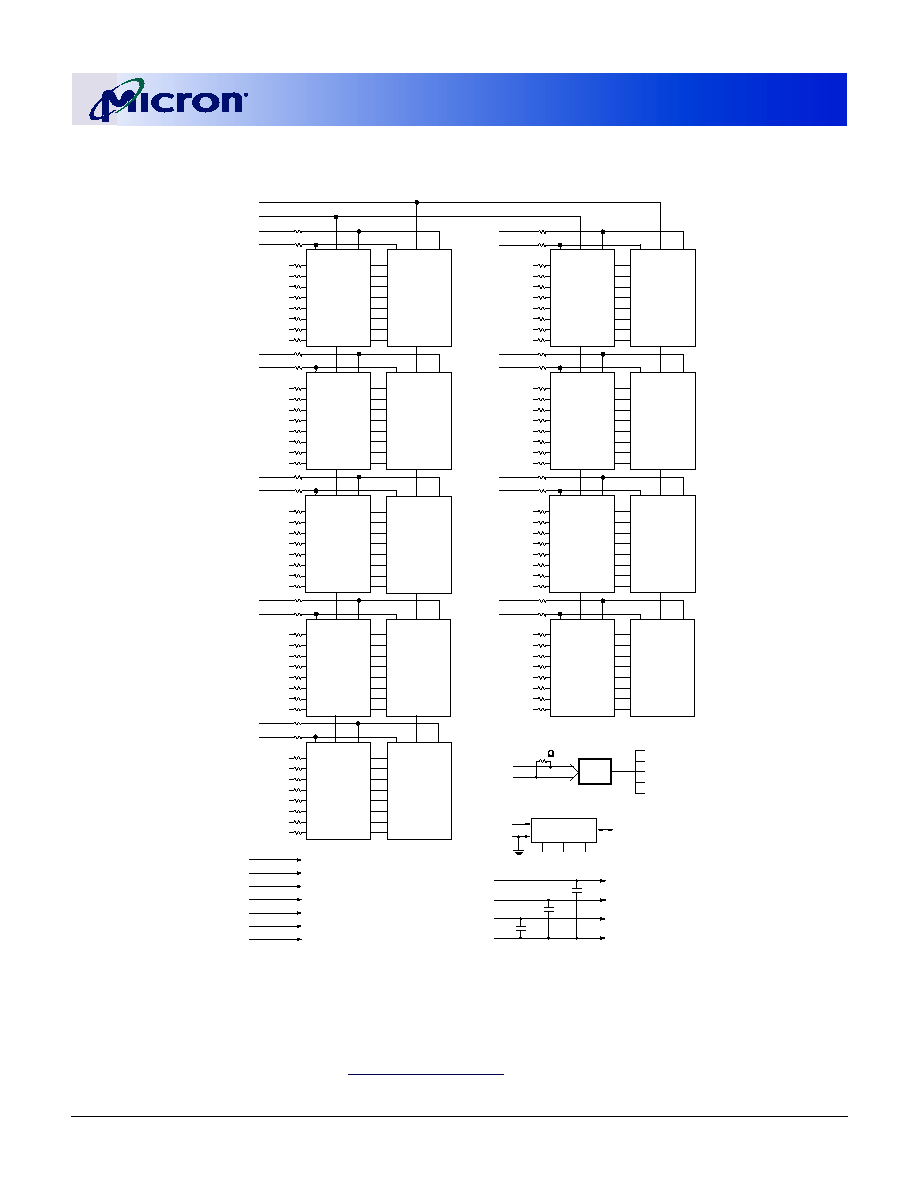
Figure 3: Functional Block Diagram
MT9VDDT1672PH, MT9VDDT3272PH, and MT9VDDT6472PH
A0
SA0
SERIAL PD
SDA
A1
SA1
A2
SA2
BA0, BA1
A0-A11
3
A0-A12
4
RAS#
BA0, BA1: DDR SDRAMS
A0-A11: DDR SDRAMS
A0-A12: DDR SDRMAS
RAS#: DDR SDRAMS
CAS#: DDR SDRAMS
CKE0: DDR SDRAMS
WE#: DDR SDRAMS
CAS#
CKE0
WE#
V
REF
V
SS
DDR SDRAMS
DDR SDRAMS
DQ56
DQ57
DQ58
DQ59
DQ60
DQ61
DQ62
DQ63
U8
DQ
DQ
DQ
DQ
DQ
DQ
DQ
DQ
DQ48
DQ49
DQ50
DQ51
DQ52
DQ53
DQ54
DQ55
U6
DQ
DQ
DQ
DQ
DQ
DQ
DQ
DQ
DQ40
DQ41
DQ42
DQ43
DQ44
DQ45
DQ46
DQ47
U5
DQ
DQ
DQ
DQ
DQ
DQ
DQ
DQ
DQ32
DQ33
DQ34
DQ35
DQ36
DQ37
DQ38
DQ39
U9
DQ
DQ
DQ
DQ
DQ
DQ
DQ
DQ
DQ24
DQ25
DQ26
DQ27
DQ28
DQ29
DQ30
DQ31
U4
DQ
DQ
DQ
DQ
DQ
DQ
DQ
DQ
DQ16
DQ17
DQ18
DQ19
DQ20
DQ21
DQ22
DQ23
U2
DQ
DQ
DQ
DQ
DQ
DQ
DQ
DQ
DQ8
DQ9
DQ10
DQ11
DQ12
DQ13
DQ14
DQ15
DM CS# DQS
U1
DQ
DQ
DQ
DQ
DQ
DQ
DQ
DQ
DQ0
DQ1
DQ2
DQ3
DQ4
DQ5
DQ6
DQ7
DM0
S0#
U3
DQ
DQ
DQ
DQ
DQ
DQ
DQ
DQ
WP
SCL
DM CS# DQS
DM CS# DQS
DM CS# DQS
DQS0
DM4
DQS4
DM1
DQS1
DM5
DQS5
DM2
DQS2
DM6
DQS6
DM CS# DQS
U7
DQ
DQ
DQ
DQ
DQ
DQ
DQ
DQ
DM CS# DQS
DM CS# DQS
DM CS# DQS
DM CS# DQS
DM3
DQS3
DM7
DQS7
DM8
DQS8
CB0
CB1
CB2
CB3
CB4
CB5
CB6
CB7
V
DDSPD
V
DD
DDR SDRAMS
SPD
U11
PLL
DDR SDRAM X 2
DDR SDRAM X 2
DDR SDRAM X 2
DDR SDRAM X 2
DDR SDRAM X 1
CK0
CK0#
120
U10
NOTE:
1. All resistor values are 22
W unless otherwise specified.
2. Per industry standard, Micron modules utilize various component speed grades, as
referenced in the module part numbering guide at
www
.
micron.com/numberguide
.
3. MT9VDDT1672PH
4. MT9VDDT3272PH, MT9VDDT6472PH
DDR SDRAMs = MT46V16M8TG for MT9VDDT1672PH
DDR SDRAMs = MT46V32M8TG for MT9VDDT3272PH
DDR SDRAMs = MT46V64M8TG for MT9VDDT6472PH
Contact Micron for information on IT modules.
128MB, 256MB, 512MB, 1GB (x72, ECC, PLL)
200-PIN DDR SDRAM SODIMM
09005aef808ffdc7
Micron Technology, Inc., reserves the right to change products or specifications without notice.
DD9_18C16_32_64_128X72PHG_E.fm - Rev. E 7/03 EN
7
�2003 Micron Technology, Inc. All rights reserved.
Figure 4: Functional Block Diagram
MT18VDDT6472PH and MT18VDDT12872PH
A0
SA0
SERIAL PD
SDA
A1
SA1
A2
SA2
BA0, BA1
A0-A12
RAS#
BA0, BA1: DDR SDRAMs
A0-A12: DDR SDRAMs
RAS#: DDR SDRAMs
CAS#: DDR SDRAMs
CKE0: DDR SDRAMs U1b-U9b
CKE1: DDR SDRAMs U1t-U9t
WE#: DDR SDRAMs
CAS#
CKE0
CKE1
WE#
V
REF
V
SS
DDR SDRAMs
DDR SDRAMs
DQ56
DQ57
DQ58
DQ59
DQ60
DQ61
DQ62
DQ63
U8b
DQ
DQ
DQ
DQ
DQ
DQ
DQ
DQ
DQ48
DQ49
DQ50
DQ51
DQ52
DQ53
DQ54
DQ55
U6b
DQ
DQ
DQ
DQ
DQ
DQ
DQ
DQ
DQ40
DQ41
DQ42
DQ43
DQ44
DQ45
DQ46
DQ47
U5b
DQ
DQ
DQ
DQ
DQ
DQ
DQ
DQ
DQ32
DQ33
DQ34
DQ35
DQ36
DQ37
DQ38
DQ39
U9b
DQ
DQ
DQ
DQ
DQ
DQ
DQ
DQ
DQ24
DQ25
DQ26
DQ27
DQ28
DQ29
DQ30
DQ31
U4b
DQ
DQ
DQ
DQ
DQ
DQ
DQ
DQ
DQ16
DQ17
DQ18
DQ19
DQ20
DQ21
DQ22
DQ23
U2b
DQ
DQ
DQ
DQ
DQ
DQ
DQ
DQ
DQ8
DQ9
DQ10
DQ11
DQ12
DQ13
DQ14
DQ15
DM CS# DQS
U1b
DQ
DQ
DQ
DQ
DQ
DQ
DQ
DQ
DQ0
DQ1
DQ2
DQ3
DQ4
DQ5
DQ6
DQ7
DM0
S0#
U3b
DQ
DQ
DQ
DQ
DQ
DQ
DQ
DQ
WP
PLL
DDR SDRAM X 4
DDR SDRAM X 4
DDR SDRAM X 4
DDR SDRAM X 4
DDR SDRAM X 2
SCL
U1t
DQ
DQ
DQ
DQ
DQ
DQ
DQ
DQ
U2t
DQ
DQ
DQ
DQ
DQ
DQ
DQ
DQ
U3t
DQ
DQ
DQ
DQ
DQ
DQ
DQ
DQ
U5t
DQ
DQ
DQ
DQ
DQ
DQ
DQ
DQ
S1#
DM CS# DQS
DM CS# DQS
DM CS# DQS
DM CS# DQS
DM CS# DQS
DM CS# DQS
DQS0
DM4
DQS4
DM1
DQS1
DM5
DQS5
U6t
DQ
DQ
DQ
DQ
DQ
DQ
DQ
DQ
DM CS# DQS
DM2
DQS2
DM6
DQS6
DM CS# DQS
DM CS# DQS
U7b
DQ
DQ
DQ
DQ
DQ
DQ
DQ
DQ
U7t
DQ
DQ
DQ
DQ
DQ
DQ
DQ
DQ
DM CS# DQS
DM CS# DQS
DM CS# DQS
DM CS# DQS
DM CS# DQS
DM3
DQS3
DM7
DQS7
U4t
DQ
DQ
DQ
DQ
DQ
DQ
DQ
DQ
DM CS# DQS
U8t
DQ
DQ
DQ
DQ
DQ
DQ
DQ
DQ
DM CS# DQS
DM8
DQS8
U9t
DQ
DQ
DQ
DQ
DQ
DQ
DQ
DQ
DM CS# DQS
CB0
CB1
CB2
CB3
CB4
CB5
CB6
CB7
V
DDSPD
V
DD
DDR SDRAMs
SPD
CK0
CK0#
120
U11
U10
DDR SDRAMs = MT46V32M8TG for MT18VDDT6472PH
DDR SDRAMs = MT46V64M8TG for MT18VDDT12872PH
Contact Micron for information on IT modules.
NOTE:
1. All resistor values are 22
W unless otherwise specified.
2. 'b' = bottom portion of stacked SDRAM, 't' = top portion of stacked SDRAM.
3. Per industry standard, Micron modules utilize various component speed grades, as
referenced in the module part numbering guide at
www.micron.com/numberguide
.

128MB, 256MB, 512MB, 1GB (x72, ECC, PLL)
200-PIN DDR SDRAM SODIMM
09005aef808ffdc7
Micron Technology, Inc., reserves the right to change products or specifications without notice.
DD9_18C16_32_64_128X72PHG_E.fm - Rev. E 7/03 EN
8
�2003 Micron Technology, Inc. All rights reserved.
General Description
The Micron MT9VDDT1672PH, MT9VDDT3272PH,
MT18VDDT6472PH, MT9VDDT6472PH, and MT18VDDT12872PH
are high-speed CMOS, dynamic random-access,
128MB, 256MB, 512MB, and 1GB memory modules
organized in x72 (ECC) configuration. DDR SDRAM
modules use internally configured quad-bank DDR
SDRAM devices.
DDR SDRAM modules use a double data rate archi-
tecture to achieve high-speed operation. The double
data rate architecture is essentially a 2n-prefetch
architecture with an interface designed to transfer two
data words per clock cycle at the I/O pins. A single
read or write access for the DDR SDRAM module effec-
tively consists of a single 2n-bit wide, one-clock-cycle
data transfer at the internal DRAM core and two corre-
sponding n-bit wide, one-half-clock-cycle data trans-
fers at the I/O pins.
A bidirectional data strobe (DQS) is transmitted
externally, along with data, for use in data capture at
the receiver. DQS is an intermittent strobe transmitted
by the DDR SDRAM device during READs and by the
memory controller during WRITEs. DQS is edge-
aligned with data for READs and center-aligned with
data for WRITEs.
DDR SDRAM modules operate from differential
clock inputs (CK and CK#); the crossing of CK going
HIGH and CK# going LOW will be referred to as the
positive edge of CK. Commands (address and control
signals) are registered at every positive edge of CK.
Input data is registered on both edges of DQS, and out-
put data is referenced to both edges of DQS, as well as
to both edges of CK. A phase-lock loop (PLL) device on
the module is used to redrive the differential clock sig-
nals to the DDR SDRAM devices to minimize system
clock loading.
Read and write accesses to DDR SDRAM modules
are burst oriented; accesses start at a selected location
and continue for a programmed number of locations in
a programmed sequence. Accesses begin with the reg-
istration of an ACTIVE command, which is then fol-
lowed by a READ or WRITE command. The address bits
registered coincident with the ACTIVE command are
used to select the device bank and row to be accessed
(BA0, BA1 select device bank; A0�A11 select device row
for the module MT9VDDT1672PH and A0�A12 select
device row for modules MT9VDDT3272PH,
MT18VDDT6472PH, MT9VDDT6472PH, and
MT18VDDT12872PH). The address bits registered
coincident with the READ or WRITE command are
used to select the device bank and the starting device
column location for the burst access.
DDR SDRAM modules provide for programmable
read or write burst lengths of 2, 4, or 8 locations. An
auto precharge function may be enabled to provide a
self-timed row precharge that is initiated at the end of
the burst access.
The pipelined, multibank architecture of DDR
SDRAM modules allows for concurrent operation,
thereby providing high effective bandwidth by hiding
row precharge and activation time.
An auto refresh mode is provided, along with a
power-saving power-down mode. All inputs are com-
patible with the JEDEC Standard for SSTL_2. All out-
puts are SSTL_2, Class II compatible. For more
information regarding DDR SDRAM operation, refer to
the 128Mb, 256Mb, and 512Mb DDR SDRAM data
sheets.
PLL Operation
A phase-lock loop (PLL) on the module is used to
redrive the differential clock signals CK and CK# to the
DDR SDRAM devices to minimize system clock load-
ing.
Serial Presence-Detect Operation
These DDR SDRAM modules incorporate serial
presence-detect (SPD). The SPD function is imple-
mented using a 2,048-bit EEPROM. This nonvolatile
storage device contains 256 bytes. The first 128 bytes
can be programmed by Micron to identify the module
type and various SDRAM organizations and timing
parameters. The remaining 128 bytes of storage are
available for use by the customer. System READ/
WRITE operations between the master (system logic)
and the slave EEPROM device (DIMM) occur via a
standard I
2
C bus using the DIMM's SCL (clock) and
SDA (data) signals, together with SA(2:0), which pro-
vide eight unique DIMM/EEPROM addresses. Write
protect (WP) is tied to ground on the module, perma-
nently disabling hardware write protect.
Mode Register Definition
The mode register is used to define the specific
mode of operation of the DDR SDRAM. This definition
includes the selection of a burst length, a burst type, a
CAS latency and an operating mode, as shown in the
Mode Register Diagram. The mode register is pro-
grammed via the MODE REGISTER SET command
(with BA0 = 0 and BA1 = 0) and will retain the stored
information until it is programmed again or the device
loses power (except for bit A8, which is self-clearing).
128MB, 256MB, 512MB, 1GB (x72, ECC, PLL)
200-PIN DDR SDRAM SODIMM
09005aef808ffdc7
Micron Technology, Inc., reserves the right to change products or specifications without notice.
DD9_18C16_32_64_128X72PHG_E.fm - Rev. E 7/03 EN
9
�2003 Micron Technology, Inc. All rights reserved.
Reprogramming the mode register will not alter the
contents of the memory, provided it is performed cor-
rectly. The mode register must be loaded (reloaded)
when all device banks are idle and no bursts are in
progress, and the controller must wait the specified
time before initiating the subsequent operation. Vio-
lating either of these requirements will result in
unspecified operation.
Mode register bits A0�A2 specify the burst length, A3
specifies the type of burst (sequential or interleaved),
A4�A6 specify the CAS latency, and A7�A11 (for
MT9VDDT1672PH) or A7�A12 (for MT9VDDT3272PH,
MT18VDDT6472PH, MT9VDDT6472PH, and MT18VDDT12872PH)
specify the operating mode.
Burst Length
Read and write accesses to the DDR SDRAM are
burst oriented, with the burst length being program-
mable, as shown in Mode Register Diagram. The burst
length determines the maximum number of column
locations that can be accessed for a given READ or
WRITE command. Burst lengths of 2, 4, or 8 locations
are available for both the sequential and the inter-
leaved burst types.
Reserved states should not be used, as unknown oper-
ation or incompatibility with future versions may result.
When a READ or WRITE command is issued, a block
of columns equal to the burst length is effectively
selected. All accesses for that burst take place within
this block, meaning that the burst will wrap within the
block if a boundary is reached. The block is uniquely
selected by A1�Ai when the burst length is set to two,
by A2�Ai when the burst length is set to four and by
A3�Ai when the burst length is set to eight (where Ai is
the most significant column address bit for a given
configuration; see note 5 of Table 6, Burst Definition
Table, on page 10). The remaining (least significant)
address bit(s) is (are) used to select the starting loca-
tion within the block. The programmed burst length
applies to both read and write bursts.
Burst Type
Accesses within a given burst may be programmed
to be either sequential or interleaved; this is referred to
as the burst type and is selected via bit M3.
The ordering of accesses within a burst is deter-
mined by the burst length, the burst type and the start-
ing column address, as shown in Table 6, Burst
Definition Table, on page 10.
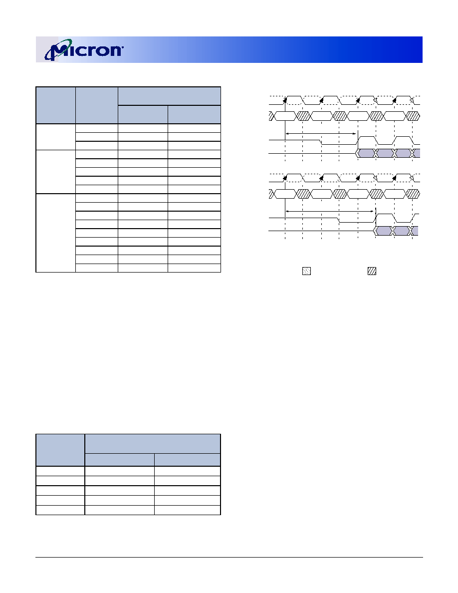
Read Latency
The READ latency is the delay, in clock cycles,
between the registration of a READ command and the
availability of the first bit of output data. The latency
can be set to 2 or 2.5 clocks, as shown in Figure 6, CAS
Latency Diagram, on page 10.
Figure 5: Mode Register Definition
Diagram
M3 = 0
Reserved
2
4
8
Reserved
Reserved
Reserved
Reserved
M3 = 1
Reserved
2
4
8
Reserved
Reserved
Reserved
Reserved
Operating Mode
Normal Operation
Normal Operation/Reset DLL
All other states reserved
0
1
-
0
0
-
0
0
-
0
0
-
0
0
-
0
0
-
Valid
Valid
-
0
1
Burst Type
Sequential
Interleaved
CAS Latency
Reserved
Reserved
2
Reserved
Reserved
Reserved
2.5
Reserved
Burst Length
M0
0
1
0
1
0
1
0
1
Burst Length
CAS Latency BT
0*
A9
A7 A6 A5 A4 A3
A8
A2 A1 A0
Mode Register (Mx)
Address Bus
9
7
6
5
4
3
8
2
1
0
M1
0
0
1
1
0
0
1
1
M2
0
0
0
0
1
1
1
1
M3
M4
0
1
0
1
0
1
0
1
M5
0
0
1
1
0
0
1
1
M6
0
0
0
0
1
1
1
1
M6-M0
M8 M7
Operating Mode
A10
A12 A11
BA0
BA1
10
11
12
13
0*
14
* M14 and M13 (BA1 and BA0)
must be "0, 0" to select the
base mode register (vs. the
extended mode register).
M9
M10
M12 M11
Burst Length
CAS Latency BT
0*
0*
A9
A7 A6 A5 A4 A3
A8
A2 A1 A0
Mode Register (Mx)
Address Bus
9
7
6
5
4
3
8
2
1
0
Operating Mode
A10
A11
BA0
BA1
10
11
12
13
* M13 and M12 (BA1and BA0) must be "0, 0" to select the
base mode register (vs. the extended mode register).
MT9VDDT1672PH Module Address Bus
MT9VDDT3272PH; MT18VDDT6472PH; MT9VDDT6472PH,
MT18VDDT12872PH Module Address Bus
128MB, 256MB, 512MB, 1GB (x72, ECC, PLL)
200-PIN DDR SDRAM SODIMM
09005aef808ffdc7
Micron Technology, Inc., reserves the right to change products or specifications without notice.
DD9_18C16_32_64_128X72PHG_E.fm - Rev. E 7/03 EN
10
�2003 Micron Technology, Inc. All rights reserved.
NOTE:
1. For a burst length of two, A1-Ai select the two- data-
element block; A0 selects the first access within the
block.
2. For a burst length of four, A2-Ai select the four- data-
element block; A0-A1 select the first access within the
block.
3. For a burst length of eight, A3-Ai select the eight-
data-element block; A0-A2 select the first access within
the block.
4. Whenever a boundary of the block is reached within a
given sequence above, the following access wraps
within the block.
5. i = 9 for MT9VDDT1672PH, MT9VDDT3272PH, and
MT18VDDT6472PH
i = 9, 11 for MT9VDDT6472PH, MT18VDDT12872PH
Figure 6: CAS Latency Diagram
If a READ command is registered at clock edge n,
and the latency is m clocks, the data will be available
nominally coincident with clock edge n + m. Table 7,
CAS Latency (CL) Table, on page 10, indicates the
operating frequencies at which each CAS latency set-
ting can be used.
Reserved states should not be used as unknown
operation or incompatibility with future versions may
result.
Operating Mode
The normal operating mode is selected by issuing a
MODE REGISTER SET command with bits A7�A11 (for
MT9VDDT1672PH), or A7�A12 (for MT9VDDT3272PH,
MT18VDDT6472PH, MT9VDDT6472PH, and MT18VDDT12872PH)
each set to zero, and bits A0�A6 set to the desired val-
ues.
A DLL reset is initiated by issuing a MODE REGIS-
TER SET command with bits A7 and A9�A11 (for
MT9VDDT1672PH), or A7 and A9�A12 (for
MT9VDDT3272PH, MT18VDDT6472PH, MT9VDDT6472PH,
and MT18VDDT12872PH) each set to zero, bit A8 set to
one, and bits A0�A6 set to the desired values. Although
not required by the Micron device, JEDEC specifica-
tions recommend when a LOAD MODE REGISTER
command is issued to reset the DLL, it should always
be followed by a LOAD MODE REGISTER command to
select normal operating mode.
Table 6:
Burst Definition Table
BURST
LENGTH
STARTING
COLUMN
ADDRESS
ORDER OF ACCESSES WITHIN
A BURST
TYPE =
SEQUENTIAL
TYPE =
INTERLEAVED
2
A0
0
0-1
0-1
1
1-0
1-0
4
A1 A0
0
0
0-1-2-3
0-1-2-3
0
1
1-2-3-0
1-0-3-2
1
0
2-3-0-1
2-3-0-1
1
1
3-0-1-2
3-2-1-0
8
A2 A1 A0
0
0
0
0-1-2-3-4-5-6-7 0-1-2-3-4-5-6-7
0
0
1
1-2-3-4-5-6-7-0 1-0-3-2-5-4-7-6
0
1
0
2-3-4-5-6-7-0-1 2-3-0-1-6-7-4-5
0
1
1
3-4-5-6-7-0-1-2 3-2-1-0-7-6-5-4
1
0
0
4-5-6-7-0-1-2-3 4-5-6-7-0-1-2-3
1
0
1
5-6-7-0-1-2-3-4 5-4-7-6-1-0-3-2
1
1
0
6-7-0-1-2-3-4-5 6-7-4-5-2-3-0-1
1
1
1
7-0-1-2-3-4-5-6 7-6-5-4-3-2-1-0
Table 7:
CAS Latency (CL) Table
SPEED
ALLOWABLE OPERATING
CLOCK FREQUENCY (MHZ)
CL = 2
CL = 2.5
-335
N/A
75
� f � 167
-262
75
� f � 133
75
� f � 133
-26A
75
� f � 133
75
� f � 133
-265
75
� f � 100
75
� f � 133
-202
75
� f � 100
N/A
CK
CK#
COMMAND
DQ
DQS
CL = 2
READ
NOP
NOP
NOP
READ
NOP
NOP
NOP
Burst Length = 4 in the cases shown
Shown with nominal tAC, tDQSCK, and tDQSQ
CK
CK#
COMMAND
DQ
DQS
CL = 2.5
T0
T1
T2
T2n
T3
T3n
T0
T1
T2
T2n
T3
T3n
DON'T CARE
TRANSITIONING DATA

128MB, 256MB, 512MB, 1GB (x72, ECC, PLL)
200-PIN DDR SDRAM SODIMM
09005aef808ffdc7
Micron Technology, Inc., reserves the right to change products or specifications without notice.
DD9_18C16_32_64_128X72PHG_E.fm - Rev. E 7/03 EN
11
�2003 Micron Technology, Inc. All rights reserved.
All other combinations of values for A7�A11, or A7�
A12 are reserved for future use and/or test modes. Test
modes and reserved states should not be used because
unknown operation or incompatibility with future ver-
sions may result.
Extended Mode Register
The extended mode register controls functions
beyond those controlled by the mode register; these
additional functions are DLL enable/disable and out-
put drive strength. These functions are controlled via
the bits shown in the Extended Mode Register Defini-
tion Diagram. The extended mode register is pro-
grammed via the LOAD MODE REGISTER command
to the mode register (with BA0 = 1 and BA1 = 0) and
will retain the stored information until it is pro-
grammed again or the device loses power. The
enabling of the DLL should always be followed by a
LOAD MODE REGISTER command to the mode regis-
ter (BA0, /BA1 both low) to reset the DLL.
The extended mode register must be loaded when
all device banks are idle and no bursts are in progress,
and the controller must wait the specified time before
initiating any subsequent operation. Violating either
of these requirements could result in unspecified oper-
ation.
DLL Enable/Disable
The DLL must be enabled for normal operation.
DLL enable is required during power-up initialization
and upon returning to normal operation after having
disabled the DLL for the purpose of debug or evalua-
tion. (When the device exits self refresh mode, the DLL
is enabled automatically.) Any time the DLL is enabled,
200 clock cycles must occur before a READ command
can be issued.
Figure 7: Extended Mode Register
Definition Diagram
NOTE:
1. E13 and E12 (MT9VDDT3272PH), or E14 and E13
(MT9VDDT6472PH, MT18VDDT6472PH,
MT9VDDT6472PH, MT18VDDT12872PH) (BA1 and BA0)
must be "0, 1" to select the Extended Mode Register
(vs. the base Mode Register).
2. The QFC# option is not supported.
Operating Mode
Reserved
Reserved
0
�
0
�
Valid
�
0
1
DLL
Enable
Disable
DLL
11
01
A9
A7 A6 A5 A4 A3
A8
A2 A1 A0
Extended Mode
Register (Ex)
Address Bus
9
7
6
5
4
3
8
2
1
0
E0
0
Drive Strength
Normal
E1
E0
E1,
Operating Mode
A10
A11
A12
BA1 BA0
10
11
12
13
14
E2,
E3
E4
0
�
0
�
0
�
0
�
0
�
E6 E5
E7
E8
E9
0
�
0
�
E10
E11
0
�
E12
DS
DLL
11
01
A9
A7 A6 A5 A4 A3
A8
A2 A1 A0
Extended Mode
Register (Ex)
Address Bus
9
7
6
5
4
3
8
2
1
0
Operating Mode
A10
A11
BA1 BA0
10
11
12
13
DS
MT9VDDT1672PH Module Address Bus
MT9VDDT3272PH; MT18VDDT6472PH; MT9VDDT6472PH,
MT18VDDT12872PH Module Address Bus
128MB, 256MB, 512MB, 1GB (x72, ECC, PLL)
200-PIN DDR SDRAM SODIMM
09005aef808ffdc7
Micron Technology, Inc., reserves the right to change products or specifications without notice.
DD9_18C16_32_64_128X72PHG_E.fm - Rev. E 7/03 EN
12
�2003 Micron Technology, Inc. All rights reserved.
Commands
Table 8, Commands Truth Table, and Table 9, DM
Operation Truth Table, provide a general reference of
available commands. For a more detailed description
of commands and operations, refer to the Micron
128Mb, 256Mb, or 512Mb DDR SDRAM component
data sheets.
NOTE:
1. DESELECT and NOP are functionally interchangeable.
2. BA0�BA1 provide device bank address and A0�A11 (MT9VDDT1672PH) or A0�A12 (MT9VDDT3272PH, MT9VDDT6472PH,
MT18VDDT6472PH, MT18VDDT12872PH) provide row address.
3. BA0�BA1 provide device bank address; A0�A8 (MT9VDDT1672PH) or A0-A9 (MT9VDDT3272PH, MT9VDDT6472PH,
MT18VDDT6472PH, MT18VDDT12872PH), provide column address; A10 HIGH enables the auto precharge feature (non-
persistent), and A10 LOW disables the auto precharge feature.
4. Applies only to read bursts with auto precharge disabled; this command is undefined (and should not be used) for READ
bursts with auto precharge enabled and for WRITE bursts.
5. A10 LOW: BA0�BA1 determine which device bank is precharged. A10 HIGH: all device banks are precharged and BA0�
BA1 are "Don't Care."
6. This command is AUTO REFRESH if CKE is HIGH, SELF REFRESH if CKE is LOW.
7. Internal refresh counter controls row addressing; all inputs and I/Os are "Don't Care" except for CKE.
8. BA0�BA1 select either the mode register or the extended mode register (BA0 = 0, BA1 = 0 select the mode register;
BA0 = 1, BA1 = 0 select extended mode register; other combinations of BA0�BA1 are reserved). A0�A11
(MT9VDDT1672PH) or A0�A12 (MT9VDDT3272PH, MT18VDDT6472PH, MT9VDDT6472PH, MT18VDDT12872PH) provide
the op-code to be written to the selected mode register.
Table 8:
Commands Truth Table
CKE is HIGH for all commands shown except SELF REFRESH
NAME (FUNCTION)
CS#
RAS# CAS#
WE#
ADDR
NOTES
DESELECT (NOP)
H
X
X
X
X
1
NO OPERATION (NOP)
L
H
H
H
X
1
ACTIVE (Select device bank and activate row)
L
L
H
H
Bank/Row
2
READ (Select device bank and column, and start READ burst)
L
H
L
H
Bank/Col
3
WRITE (Select device bank and column, and start WRITE burst)
L
H
L
L
Bank/Col
3
BURST TERMINATE
L
H
H
L
X
4
PRECHARGE (Deactivate row in device bank or banks)
L
L
H
L
Code
5
AUTO REFRESH or SELF REFRESH
(Enter self refresh mode)
L
L
L
H
X
6, 7
LOAD MODE REGISTER
L
L
L
L
Op-Code
8
Table 9:
DM Operation Truth Table
Used to mask write data; provided coincident with the corresponding data
NAME (FUNCTION)
DM
DQS
Write Enable
L
Valid
Write Inhibit
H
X

128MB, 256MB, 512MB, 1GB (x72, ECC, PLL)
200-PIN DDR SDRAM SODIMM
09005aef808ffdc7
Micron Technology, Inc., reserves the right to change products or specifications without notice.
DD9_18C16_32_64_128X72PHG_E.fm - Rev. E 7/03 EN
13
�2003 Micron Technology, Inc. All rights reserved.
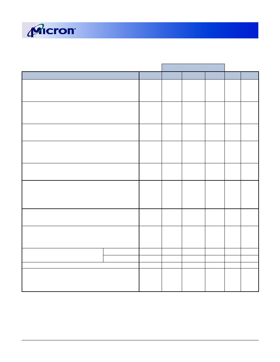
Absolute Maximum Ratings
Stresses greater than those listed may cause perma-
nent damage to the device. This is a stress rating only,
and functional operation of the device at these or any
other conditions above those indicated in the opera-
tional sections of this specification is not implied.
Exposure to absolute maximum rating conditions for
extended periods may affect reliability.
V
DD
Supply Voltage Relative to V
SS
. . . . -1V to +3.6V
V
DD
Q Supply Voltage Relative to V
SS
. . . -1V to +3.6V
V
REF
and Inputs Voltage
Relative to Vss . . . . . . . . . . . . . . . . . . . . -1V to +3.6V
I/O Pins Voltage
Relative to V
SS
. . . . . . . . . . . . . -0.5V to VddQ +0.5V
Operating Temperature,
T
A
(commercial). . . . . . . . . . . . . . . . . . .0�C to +70�C
T
A
(industrial) . . . . . . . . . . . . . . . . . . .-40�C to +85�C
Storage Temperature (plastic) . . . . . . -55�C to +150�C
Power Dissipation
Single-Rank Module . . . . . . . . . . . . . . . . . . . . . . . 9W
Dual-Rank Module . . . . . . . . . . . . . . . . . . . . . . . 18W
Short Circuit Output Current. . . . . . . . . . . . . . . . 50mA
Table 10: DC Electrical Characteristics and Operating Conditions
(MT9VDDT1672PH, MT9VDDT3272PH, and MT9VDDT6472PH)
Notes: 1�5, 14, 48; notes appear on pages 24�27; 0
�C � T
A
� +70�C
PARAMETER/CONDITION
SYMBOL
MIN
MAX
UNITS
NOTES
Supply Voltage
V
DD
2.3
2.7
V
32, 36
I/O Supply Voltage
V
DDQ
2.3
2.7
V
32, 36, 39
I/O Reference Voltage
V
REF
0.49 x V
DDQ
0.51 x V
DDQ
V
6, 39
I/O Termination Voltage (system)
V
TT
V
REF
- 0.04
V
REF
+ 0.04
V
7, 39
Input High (Logic 1) Voltage
V
IH
(D
C
)
V
REF
+ 0.15
V
DD
+ 0.3
V
25
Input Low (Logic 0) Voltage
V
IL
(
DC
)
-0.3
V
REF
- 0.15
V
25
INPUT LEAKAGE CURRENT
Any input 0V
� V
IN
� V
DD
, V
REF
pin 0V
� V
IN
�
1.35V
(All other pins not under test = 0V)
Command/Address,
RAS#, CAS#, WE#,
CKE, S#
I
I
-18
18
�A
47
CK, CK#
I
I
-5
5
�A
DM
I
I
-2
2
�A
OUTPUT LEAKAGE CURRENT
(DQs are disabled; 0V
� V
OUT
� V
DDQ
)
DQS, DQ
I
OZ
-5
5
�A
47
OUTPUT LEVELS:
High Current (V
OUT
= V
DDQ
-0.373V, minimum V
REF
, minimum V
TT
)
Low Current (V
OUT
= 0.373V, maximum V
REF
, maximum V
TT
)
I
OH
-16.8
�
mA
33, 34
I
OL
16.8
�
mA
128MB, 256MB, 512MB, 1GB (x72, ECC, PLL)
200-PIN DDR SDRAM SODIMM
09005aef808ffdc7
Micron Technology, Inc., reserves the right to change products or specifications without notice.
DD9_18C16_32_64_128X72PHG_E.fm - Rev. E 7/03 EN
14
�2003 Micron Technology, Inc. All rights reserved.
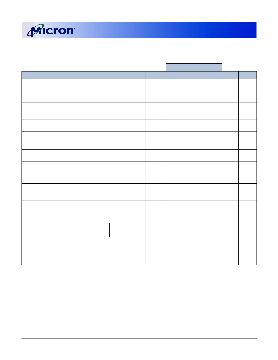
Table 11: DC Electrical Characteristics and Operating Conditions
(MT18VDDT6472PH, MT18VDDT12872PH)
Notes: 1�5, 14, 48; notes appear on pages 24�27; 0
�C � T
A
� +70�C; V
DD
= V
DD
Q = +2.5V �0.2V
PARAMETER/CONDITION
SYMBOL
MIN
MAX
UNITS
NOTES
Supply Voltage
V
DD
2.3
2.7
V
32, 36
I/O Supply Voltage
V
DD
Q
2.3
2.7
V
32, 36, 39
I/O Reference Voltage
V
REF
0.49 x
V
DDQ
0.51 x V
DDQ
V
6, 39
I/O Termination Voltage (system)
V
TT
V
REF
- 0.04
V
REF
+ 0.04
V
7, 39
Input High (Logic 1) Voltage
V
IH
(
DC
)
V
REF
+ 0.15
V
DD
+ 0.3
V
25
Input Low (Logic 0) Voltage
V
IL
(
DC
)
-0.3
V
REF
- 0.15
V
25
INPUT LEAKAGE CURRENT
Any input 0V
� V
IN
� V
DD
, V
REF
pin 0V
� V
IN
� 1.35V
(All other pins not under test = 0V)
Command/Address,
RAS#, CAS#, WE#,
CKE
I
I
-36
36
�A
47
S#
I
I
-18
18
�A
CK,CK#
I
I
-5
5
�A
DM
I
I
-4
4
�A
OUTPUT LEAKAGE CURRENT
(DQ disabled; 0V
� V
OUT
� V
DDQ
)
DQS, DQ
I
OZ
-10
10
�A
47
OUTPUT LEVELS:
High Current (V
OUT
= V
DDQ
-0.373V, minimum V
REF
, minimum V
TT
)
Low Current (V
OUT
= 0.373V, maximum V
REF
, maximum V
TT
)
I
OH
-16.8
�
mA
33, 34
I
OL
16.8
�
mA
Table 12: AC Input Operating Conditions
Notes: 1�5, 14, 48; notes appear on pages 24�27; 0
�C � T
A
� +70�C; V
DD
= V
DD
Q = +2.5V �0.2V
PARAMETER/CONDITION
SYMBOL
MIN
MAX
UNITS
NOTES
Input High (Logic 1) Voltage
V
IH
(A
C
)
V
REF
+ 0.310
�
V
12, 25, 35
Input Low (Logic 0) Voltage
V
IL
(
AC
)
�
V
REF
- 0.310
V
12, 25, 35
I/O Reference Voltage
V
REF
(
AC
)
0.49 x V
DDQ
0.51 x
V
DDQ
V
6
128MB, 256MB, 512MB, 1GB (x72, ECC, PLL)
200-PIN DDR SDRAM SODIMM
09005aef808ffdc7
Micron Technology, Inc., reserves the right to change products or specifications without notice.
DD9_18C16_32_64_128X72PHG_E.fm - Rev. E 7/03 EN
15
�2003 Micron Technology, Inc. All rights reserved.
Table 13: I
DD
Specifications and Conditions (MT9VDDT1672PH)
DDR SDRAM components only;
Notes: 1�5, 8, 10, 12, 48; notes appear on pages 24�27; 0
�C � T
A
� +70�C; V
DD
= V
DD
Q = +2.5V �0.2V
MAX
PARAMETER/CONDITION
SYMBOL
-335
-26A/-265
-202
UNITS
NOTES
OPERATING CURRENT: One device bank; Active-Precharge;
t
RC =
t
RC (MIN);
t
CK =
t
CK (MIN); DQ, DM and DQS inputs
changing once per clock cyle; Address and control inputs
changing once every two clock cycles
I
DD0
1,125
945
945
mA
20, 42
OPERATING CURRENT: One device bank; Active-Read-
Precharge; Burst
= 2
;
t
RC =
t
RC (MIN);
t
CK =
t
CK (MIN); I
OUT
=
0mA; Address and control inputs changing once per clock
cycle
I
DD1
1,215
1,080
1,080
mA
20, 42
PRECHARGE POWER-DOWN STANDBY CURRENT: All device
banks idle; Power-down mode;
t
CK =
t
CK (MIN);
CKE = (LOW)
I
DD2P
27
27
27
mA
21, 28,
44
IDLE STANDBY CURRENT: CS# = HIGH; All device banks idle;
t
CK =
t
CK MIN; CKE = HIGH; Address and other control
inputs changing once per clock cycle. V
IN
= V
REF
for DQ, DQS,
and DM
I
DD2F
405
360
360
mA
45
ACTIVE POWER-DOWN STANDBY CURRENT: One device
bank active; Power-down mode;
t
CK =
t
CK (MIN);
CKE = LOW
I
DD3P
225
180
180
mA
21, 28,
44
ACTIVE STANDBY CURRENT: CS# = HIGH; CKE = HIGH; One
device bank; Active-Precharge;
t
RC = RAS (MAX);
t
CK =
t
CK (MIN); DQ, DM and DQS inputs changing twice per
clock cycle; Address and other control inputs changing once
per clock cycle
I
DD3N
450
405
405
mA
41
OPERATING CURRENT: Burst = 2; Reads; Continuous burst;
One device bank active; Address and control inputs
changing once per clock cycle; CK =
t
CK (MIN); I
OUT
= 0mA
I
DD4R
1,260
1,125
1,125
mA
20, 42
OPERATING CURRENT: Burst = 2; Writes; Continuous burst;
One device bank active; Address and control inputs
changing once per clock cycle;
t
CK =
t
CK (MIN); DQ, DM, and
DQS inputs changing twice per clock cycle
I
DD4W
1,260
1,080
1,080
mA
20
AUTO REFRESH CURRENT
t
RC =
t
RFC (MIN)
I
DD5
2,385
1,980
1,980
mA
20, 44
t
RFC = 15.625�s
I
DD5A
45
45
45
mA
24, 44
SELF REFRESH CURRENT: CKE
� 0.2V
I
DD6
18
18
18
mA
9
OPERATING CURRENT: Four bank interleaving READs (BL=4)
with auto precharge with,
t
RC =
t
RC (MIN);
t
CK =
t
CK (MIN); Address and control inputs change only
during Active READ, or WRITE commands
I
DD7
3,195
2,925
2,925
mA
20, 43

128MB, 256MB, 512MB, 1GB (x72, ECC, PLL)
200-PIN DDR SDRAM SODIMM
09005aef808ffdc7
Micron Technology, Inc., reserves the right to change products or specifications without notice.
DD9_18C16_32_64_128X72PHG_E.fm - Rev. E 7/03 EN
16
�2003 Micron Technology, Inc. All rights reserved.
Table 14: I
DD
Specifications and Conditions (MT9VDDT3272PH)
DDR SDRAM components only;
Notes: 1�5, 8, 10, 12, 48; notes appear on pages 24�27 ; 0
�C � T
A
� +70�C; V
DD
= V
DD
Q = +2.5V �0.2V
MAX
PARAMETER/CONDITION
SYMBOL
-335
-26A/-265
-202
UNITS
NOTES
OPERATING CURRENT: One device bank; Active-Precharge;
t
RC =
t
RC (MIN);
t
CK =
t
CK (MIN); DQ, DM and DQS inputs
changing once per clock cyle; Address and control inputs
changing once every two clock cycles
I
DD0
1,125
945
1,080
mA
20, 42
OPERATING CURRENT: One device bank; Active-Read-
Precharge; Burst
= 4
;
t
RC =
t
RC (MIN);
t
CK =
t
CK (MIN);
I
OUT
= 0mA; Address and control inputs changing once per
clock cycle
I
DD1
1,530
1,305
1,395
mA
20, 42
PRECHARGE POWER-DOWN STANDBY CURRENT: All device
banks idle; Power-down mode;
t
CK =
t
CK (MIN);
CKE = (LOW)
I
DD2P
35
36
36
mA
21, 28,
44
IDLE STANDBY CURRENT: CS# = HIGH; All device banks idle;
t
CK =
t
CK MIN; CKE = HIGH; Address and other control inputs
changing once per clock cycle. V
IN
= V
REF
for DQ, DQS, and
DM
I
DD2F
450
405
405
mA
45
ACTIVE POWER-DOWN STANDBY CURRENT: One device
bank active; Power-down mode;
t
CK =
t
CK (MIN);
CKE = LOW
I
DD3P
270
225
270
mA
21, 28,
44
ACTIVE STANDBY CURRENT: CS# = HIGH; CKE = HIGH; One
device bank; Active-Precharge;
t
RC = RAS (MAX);
t
CK =
t
CK
(MIN); DQ, DM and DQS inputs changing twice per clock
cycle; Address and other control inputs changing once per
clock cycle
I
DD3N
540
450
450
mA
41
OPERATING CURRENT: Burst = 2; Reads; Continuous burst;
One device bank active; Address and control inputs
changing once per clock cycle; CK =
t
CK (MIN); I
OUT
= 0mA
I
DD4R
1,575
1,350
1,575
mA
20, 42
OPERATING CURRENT: Burst = 2; Writes; Continuous burst;
One device bank active; Address and control inputs
changing once per clock cycle;
t
CK =
t
CK (MIN); DQ, DM, and
DQS inputs changing twice per clock cycle
I
DD4W
1,395
1,215
1,710
mA
20
AUTO REFRESH CURRENT
t
RC =
t
RFC (MIN)
I
DD5
2,295
2,115
2,205
mA
20, 44
t
RFC = 7.8125�s
I
DD5A
54
54
54
mA
24, 44
SELF REFRESH CURRENT: CKE
� 0.2V
I
DD6
36
36
36
mA
9
OPERATING CURRENT: Four bank interleaving READs (BL=4)
with auto precharge with,
t
RC =
t
RC (MIN);
t
CK =
t
CK (MIN);
Address and control inputs change only during Active READ,
or WRITE commands
I
DD7
3,645
3,150
3,285
mA
20, 43
128MB, 256MB, 512MB, 1GB (x72, ECC, PLL)
200-PIN DDR SDRAM SODIMM
09005aef808ffdc7
Micron Technology, Inc., reserves the right to change products or specifications without notice.
DD9_18C16_32_64_128X72PHG_E.fm - Rev. E 7/03 EN
17
�2003 Micron Technology, Inc. All rights reserved.
Table 15: I
DD
Specifications and Conditions (MT9VDDT6472PH)
DDR SDRAM components only;
Notes: 1�5, 8, 10, 12, 48; notes appear on pages 24�27; 0
�C � T
A
� +70�C; V
DD
= V
DD
Q = +2.5V �0.2V
MAX
PARAMETER/CONDITION
SYMBOL
-335
-26A/-265
-202
UNITS
NOTES
OPERATING CURRENT: One device bank; Active-Precharge;
t
RC =
t
RC (MIN);
t
CK =
t
CK (MIN); DQ, DM and DQS inputs changing
once per clock cyle; Address and control inputs changing once
every two clock cycles
I
DD0
1,170
1,305
1,305
mA
20, 42
OPERATING CURRENT: One device bank; Active-Read-Precharge;
Burst
= 4
;
t
RC =
t
RC (MIN);
t
CK =
t
CK (MIN); I
OUT
= 0mA; Address
and control inputs changing once per clock cycle
I
DD1
1,440
1,305
1,305
mA
20, 42
PRECHARGE POWER-DOWN STANDBY CURRENT: All device
banks idle; Power-down mode;
t
CK =
t
CK (MIN); CKE = (LOW)
I
DD2P
45
45
45
mA
21, 28,
44
IDLE STANDBY CURRENT: CS# = HIGH; All device banks idle;
t
CK
=
t
CK MIN; CKE = HIGH; Address and other control inputs
changing once per clock cycle. V
IN
= V
REF
for DQ, DQS, and DM
I
DD2F
405
360
360
mA
45
ACTIVE POWER-DOWN STANDBY CURRENT: One device bank
active; Power-down mode;
t
CK =
t
CK (MIN); CKE = LOW
I
DD3P
315
270
270
mA
21, 28,
44
ACTIVE STANDBY CURRENT: CS# = HIGH; CKE = HIGH; One
device bank; Active-Precharge;
t
RC = RAS (MAX);
t
CK =
t
CK
(MIN); DQ, DM and DQS inputs changing twice per clock cycle;
Address and other control inputs changing once per clock cycle
I
DD3N
405
360
360
mA
41
OPERATING CURRENT: Burst = 2; Reads; Continuous burst; One
device bank active; Address and control inputs changing once
per clock cycle; CK =
t
CK (MIN); I
OUT
= 0mA
I
DD4R
1,485
1,305
1,305
mA
20, 42
OPERATING CURRENT: Burst = 2; Writes; Continuous burst; One
device bank active; Address and control inputs changing once
per clock cycle;
t
CK =
t
CK (MIN); DQ, DM, and DQS inputs
changing twice per clock cycle
I
DD4W
1,395
1,215
1,215
mA
20
AUTO REFRESH CURRENT
t
RC =
t
RFC (MIN)
I
DD5
2,610
2,520
2,520
mA
20, 44
t
RFC = 7.8125�s
I
DD5A
90
90
90
mA
24, 44
SELF REFRESH CURRENT: CKE
� 0.2V
I
DD6
45
45
45
mA
9
OPERATING CURRENT: Four bank interleaving READs (BL=4) with
auto precharge with,
t
RC =
t
RC (MIN);
t
CK =
t
CK (MIN); Address
and control inputs change only during Active READ, or WRITE
commands
I
DD7
3,645
3,150
3,150
mA
20, 43
128MB, 256MB, 512MB, 1GB (x72, ECC, PLL)
200-PIN DDR SDRAM SODIMM
09005aef808ffdc7
Micron Technology, Inc., reserves the right to change products or specifications without notice.
DD9_18C16_32_64_128X72PHG_E.fm - Rev. E 7/03 EN
18
�2003 Micron Technology, Inc. All rights reserved.
NOTE:
a - Value calculated as one module rank in this operating condition, and all other module ranks in I
DD2P
(CKE LOW) Mode.
b - Value calculated reflects all module ranks in this operating condition.
Table 16: I
DD
Specifications and Conditions (MT18VDDT6472PH)
DDR SDRAM components only;
Notes: 1�5, 8, 10, 12, 48; notes appear on pages 24�27; 0
�C � T
A
� +70�C; V
DD
= V
DD
Q = +2.5V �0.2V
MAX
PARAMETER/CONDITION
SYMBOL
-26A/-265
UNITS
NOTES
OPERATING CURRENT: One device bank; Active-Precharge;
t
RC =
t
RC (MIN);
t
CK =
t
CK (MIN); DQ, DM and DQS inputs changing once per clock cyle;
Address and control inputs changing once every two clock cycles
I
DD0
a
981
mA
20, 42
OPERATING CURRENT: One device bank; Active-Read-Precharge; Burst
= 4
;
t
RC =
t
RC (MIN);
t
CK =
t
CK (MIN); I
OUT
= 0mA; Address and control inputs
changing once per clock cycle
I
DD1
a
1,341
mA
20, 42
PRECHARGE POWER-DOWN STANDBY CURRENT: All device banks idle;
Power-down mode;
t
CK =
t
CK (MIN); CKE = (LOW)
I
DD2P
b
72
mA
21, 28,
44
IDLE STANDBY CURRENT: CS# = HIGH; All device banks idle;
t
CK =
t
CK MIN;
CKE = HIGH; Address and other control inputs changing once per clock
cycle. V
IN
= V
REF
for DQ, DQS, and DM
I
DD2F
b
810
mA
45
ACTIVE POWER-DOWN STANDBY CURRENT: One device bank active;
Power-down mode;
t
CK =
t
CK (MIN); CKE = LOW
I
DD3P
b
450
mA
21, 28,
44
ACTIVE STANDBY CURRENT: CS# = HIGH; CKE = HIGH; One device bank;
Active-Precharge;
t
RC = RAS (MAX);
t
CK =
t
CK (MIN); DQ, DM and DQS
inputs changing twice per clock cycle; Address and other control inputs
changing once per clock cycle
I
DD3N
b
900
mA
41
OPERATING CURRENT: Burst = 2; Reads; Continuous burst; One device
bank active; Address and control inputs changing once per clock cycle; CK
=
t
CK (MIN); I
OUT
= 0mA
I
DD4R
a
1,386
mA
20, 42
OPERATING CURRENT: Burst = 2; Writes; Continuous burst; One device
bank active; Address and control inputs changing once per clock cycle;
t
CK
=
t
CK (MIN); DQ, DM, and DQS inputs changing twice per clock cycle
I
DD4W
a
1,251
mA
20
AUTO REFRESH CURRENT
t
RC =
t
RFC (MIN)
I
DD5
b
4,230
mA
20, 44
t
RFC = 7.8125�s
I
DD5A
b
108
mA
24, 44
SELF REFRESH CURRENT: CKE
� 0.2V
I
DD6
b
72
mA
9
OPERATING CURRENT: Four bank interleaving READs (BL=4) with auto
precharge with,
t
RC =
t
RC (MIN);
t
CK =
t
CK (MIN); Address and control
inputs change only during Active READ, or WRITE commands
I
DD7
a
3,186
mA
20, 43

128MB, 256MB, 512MB, 1GB (x72, ECC, PLL)
200-PIN DDR SDRAM SODIMM
09005aef808ffdc7
Micron Technology, Inc., reserves the right to change products or specifications without notice.
DD9_18C16_32_64_128X72PHG_E.fm - Rev. E 7/03 EN
19
�2003 Micron Technology, Inc. All rights reserved.
NOTE:
a - Value calculated as one module rank in this operating condition, and all other module ranks in I
DD2P
(CKE LOW) Mode.
b - Value calculated reflects all module ranks in this operating condition.
Table 17: I
DD
Specifications and Conditions (MT18VDDT12872PH)
DDR SDRAM components only;
Notes: 1�5, 8, 10, 12, 48; notes appear on pages 24�27; 0
�C � T
A
� +70�C; V
DD
= V
DD
Q = +2.5V �0.2V
MAX
PARAMETER/CONDITION
SYMBOL
-26A/-265
UNITS
NOTES
OPERATING CURRENT: One device bank; Active-Precharge;
t
RC =
t
RC
(MIN);
t
CK =
t
CK (MIN); DQ, DM and DQS inputs changing once per clock
cyle; Address and control inputs changing once every two clock cycles
I
DD0
a
1,080
mA
20, 42
OPERATING CURRENT: One device bank; Active-Read-Precharge; Burst
= 4
;
t
RC =
t
RC (MIN);
t
CK =
t
CK (MIN); I
OUT
= 0mA; Address and control inputs
changing once per clock cycle
I
DD1
a
1,350
mA
20, 42
PRECHARGE POWER-DOWN STANDBY CURRENT: All device banks idle;
Power-down mode;
t
CK =
t
CK (MIN); CKE = (LOW)
I
DD2P
b
90
mA
21, 28, 44
IDLE STANDBY CURRENT: CS# = HIGH; All device banks idle;
t
CK =
t
CK
MIN; CKE = HIGH; Address and other control inputs changing once per
clock cycle. V
IN
= V
REF
for DQ, DQS, and DM
I
DD2F
b
720
mA
45
ACTIVE POWER-DOWN STANDBY CURRENT: One device bank active;
Power-down mode;
t
CK =
t
CK (MIN); CKE = LOW
I
DD3P
b
540
mA
21, 28, 44
ACTIVE STANDBY CURRENT: CS# = HIGH; CKE = HIGH; One device bank;
Active-Precharge;
t
RC = RAS (MAX);
t
CK =
t
CK (MIN); DQ, DM and DQS
inputs changing twice per clock cycle; Address and other control inputs
changing once per clock cycle
I
DD3N
b
720
mA
41
OPERATING CURRENT: Burst = 2; Reads; Continuous burst; One device
bank active; Address and control inputs changing once per clock cycle; CK
=
t
CK (MIN); I
OUT
= 0mA
I
DD4R
a
1,350
mA
20, 42
OPERATING CURRENT: Burst = 2; Writes; Continuous burst; One device
bank active; Address and control inputs changing once per clock cycle;
t
CK =
t
CK (MIN); DQ, DM, and DQS inputs changing twice per clock cycle
I
DD4W
a
1,260
mA
20
AUTO REFRESH CURRENT
t
RC =
t
RFC (MIN)
I
DD5
b
5,040
mA
20, 44
t
RFC = 7.8125�s
I
DD5A
b
180
mA
24, 44
SELF REFRESH CURRENT: CKE
� 0.2V
I
DD6
b
90
mA
9
OPERATING CURRENT: Four bank interleaving READs (BL=4) with auto
precharge with,
t
RC =
t
RC (MIN);
t
CK =
t
CK (MIN); Address and control
inputs change only during Active READ, or WRITE commands
I
DD7
a
3,195
mA
20, 43

128MB, 256MB, 512MB, 1GB (x72, ECC, PLL)
200-PIN DDR SDRAM SODIMM
09005aef808ffdc7
Micron Technology, Inc., reserves the right to change products or specifications without notice.
DD9_18C16_32_64_128X72PHG_E.fm - Rev. E 7/03 EN
20
�2003 Micron Technology, Inc. All rights reserved.
Table 18: Capacitance (MT9VDDT1672PH, MT9VDDT3272PH, and MT9VDDT6472PH)
Note: 11; notes appear on pages 24�27
PARAMETER
SYMBOL
MIN
TYP
MAX
UNITS
Input/Output Capacitance: DQ, DQS, DM
C
IO
4.0
-
5.0
pF
Input Capacitance: Command and Address
C
I1
18.0
-
27.0
pF
Input Capacitance: S#
C
I2
18.0
-
27.0
pF
Input Capacitance: CK, CK#
C
I3
-
3
-
pF
Input Capacitance: CKE
C
I4
18.0
-
27.0
pF
Table 19: Capacitance (MT18VDDT6472PH and MT18VDDT12872PH)
Note: 11; notes appear on pages 24�27
PARAMETER
SYMBOL
MIN
TYP
MAX
UNITS
Input/Output Capacitance: DQ, DQS, DM
C
IO
8.0
-
10.0
pF
Input Capacitance: Command and Address
C
I1
36.0
-
54.0
pF
Input Capacitance: S#
C
I2
18.0
-
27.0
pF
Input Capacitance: CK, CK#
C
I3
-
3
-
pF
Input Capacitance: CKE
C
I4
18.0
-
27.0
pF
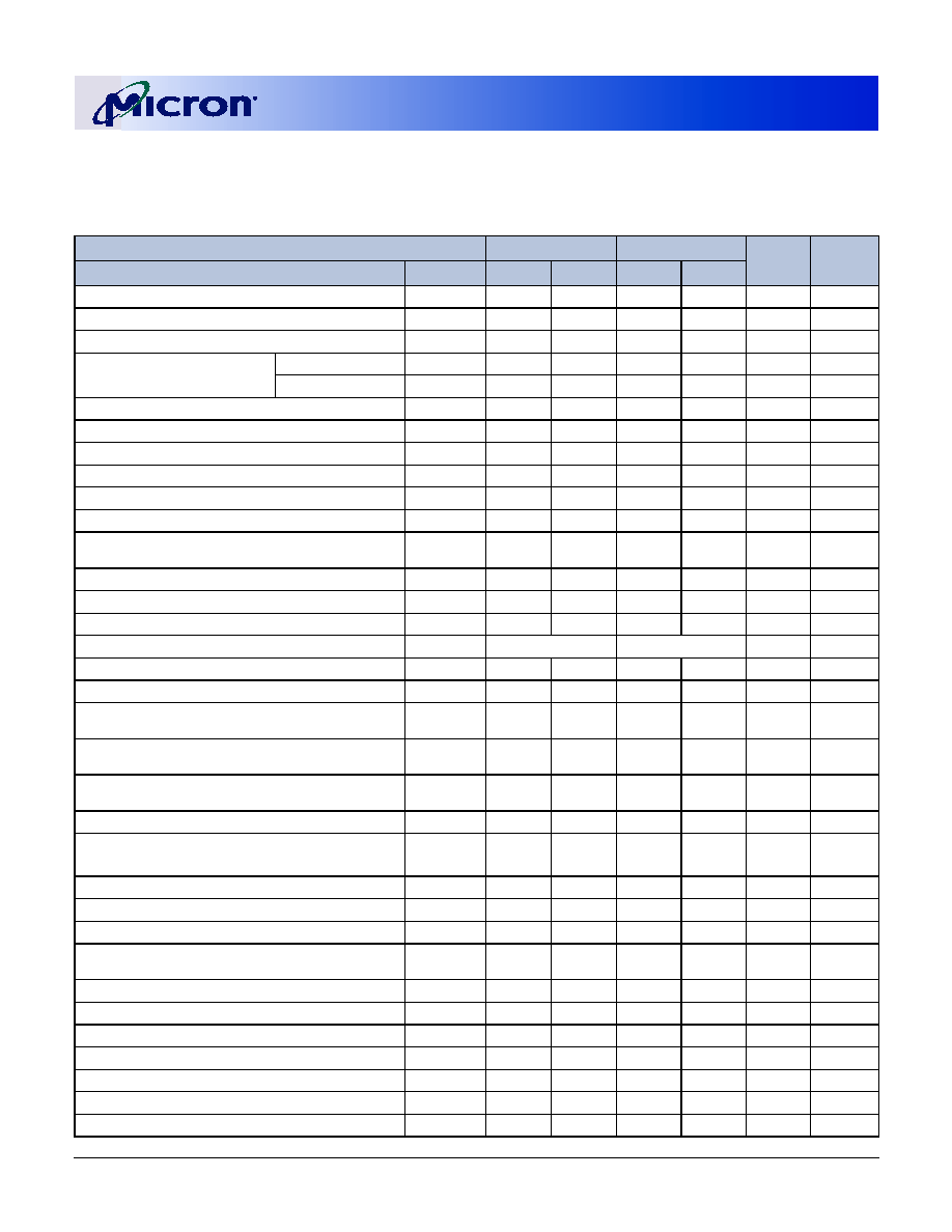
128MB, 256MB, 512MB, 1GB (x72, ECC, PLL)
200-PIN DDR SDRAM SODIMM
09005aef808ffdc7
Micron Technology, Inc., reserves the right to change products or specifications without notice.
DD9_18C16_32_64_128X72PHG_E.fm - Rev. E 7/03 EN
21
�2003 Micron Technology, Inc. All rights reserved.
Table 20: Electrical Characteristics and Recommended AC Operating Conditions
(-335 and -262)
DDR SDRAM components only; notes appear on pages 24�27
Notes: 1�5, 12�15, 29, 48; 0
�C � T
A
� +70�C; V
DD
= V
DD
Q = +2.5V �0.2V
AC CHARACTERISTICS
-335
-262
UNITS
NOTES
PARAMETER
SYMBOL
MIN
MAX
MIN
MAX
Access window of DQs from CK/CK#
t
AC
-0.7
+0.7
-0.75
+0.75
ns
CK high-level width
t
CH
0.45
0.55
0.45
0.55
t
CK
26
CK low-level width
t
CL
0.45
0.55
0.45
0.55
t
CK
26
Clock cycle time
CL = 2.5
t
CK (2.5)
6
13
7.5
13
ns
40, 46
CL = 2
t
CK (2)
7.5
13
7.5
13
ns
40, 46
DQ and DM input hold time relative to DQS
t
DH
0.45
0.5
ns
23, 27
DQ and DM input setup time relative to DQS
t
DS
0.45
0.5
ns
23, 27
DQ and DM input pulse width (for each input)
t
DIPW
1.75
1.75
ns
27
Access window of DQS from CK/CK#
t
DQSCK
-0.60
+0.60
-0.75
+0.75
ns
DQS input high pulse width
t
DQSH
0.35
0.35
t
CK
DQS input low pulse width
t
DQSL
0.35
0.35
t
CK
DQS-DQ skew, DQS to last DQ valid, per group,
per access
t
DQSQ
0.45
0.5
ns
22, 23
Write command to first DQS latching transition
t
DQSS
0.75
1.25
0.75
1.25
t
CK
DQS falling edge to CK rising - setup time
t
DSS
0.2
0.2
t
CK
DQS falling edge from CK rising - hold time
t
DSH
0.2
0.2
t
CK
Half clock period
t
HP
t
CH,
t
CL
t
CH,
t
CL
ns
30
Data-out high-impedance window from CK/CK#
t
HZ
+0.70
+0.75
ns
16, 37
Data-out low-impedance window from CK/CK#
t
LZ
-0.70
-0.75
ns
16, 38
Address and control input hold time (slow slew
rate)
t
IH
S
0.75
0.90
ns
12
Address and control input setup time (slow slew
rate)
t
IS
S
0.75
0.90
ns
12
Address and Control input pulse width (for each
input)
t
IPW
2.2
2.2
ns
LOAD MODE REGISTER command cycle time
t
MRD
0.80
15
ns
DQ-DQS hold, DQS to first DQ to go non-valid, per
access
t
QH
t
HP -
t
QHS
t
HP -
t
QHS
ns
22, 23
Data Hold Skew Factor
t
QHS
0.50
0.75
ns
ACTIVE to PRECHARGE command
t
RAS
42
70,000
40
120,000
ns
31
ACTIVE to READ with Auto precharge command
t
RAP
18
15
ns
ACTIVE to ACTIVE/AUTO REFRESH command
period
t
RC
60
60
ns
AUTO REFRESH command period
t
RFC
72
75
ns
44
ACTIVE to READ or WRITE delay
t
RCD
18
15
ns
PRECHARGE command period
t
RP
18
15
ns
DQS read preamble
t
RPRE
0.9
1.1
0.9
1.1
t
CK
37
DQS read postamble
t
RPST
0.4
0.6
0.4
0.6
t
CK
ACTIVE bank a to ACTIVE bank b command
t
RRD
12
15
ns
DQS write preamble
t
WPRE
0.25
0.25
t
CK
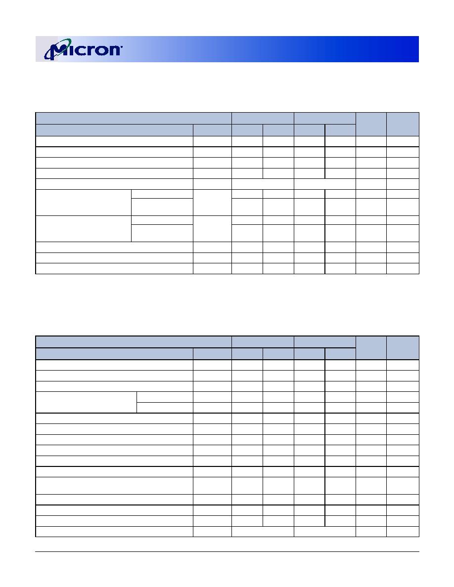
128MB, 256MB, 512MB, 1GB (x72, ECC, PLL)
200-PIN DDR SDRAM SODIMM
09005aef808ffdc7
Micron Technology, Inc., reserves the right to change products or specifications without notice.
DD9_18C16_32_64_128X72PHG_E.fm - Rev. E 7/03 EN
22
�2003 Micron Technology, Inc. All rights reserved.
DQS write preamble setup time
t
WPRES
0
0
ns
18, 19
DQS write postamble
t
WPST
0.4
0.6
0.4
0.6
t
CK
17
Write recovery time
t
WR
15
15
ns
Internal WRITE to READ command delay
t
WTR
1
1
t
CK
Data valid output window (DVW)
na
t
QH -
t
DQSQ
t
QH -
t
DQSQ
ns
22
REFRESH to REFRESH
command interval
MT9VDDT1672PH
t
REFC
140.6
140.6
�s
21
MT9VDDT3272PH
MT9VDDT6472PH
70.3
70.3
�s
21
Average periodic refresh
interval
MT9VDDT1672PH
t
REFI
15.6
15.6
�s
21
MT9VDDT3272PH
MT9VDDT6472PH
7.8
7.8
�s
Terminating voltage delay to V
DD
t
VTD
0
0
ns
Exit SELF REFRESH to non-READ command
t
XSNR
75
75
ns
Exit SELF REFRESH to READ command
t
XSRD
200
200
t
CK
Table 20: Electrical Characteristics and Recommended AC Operating Conditions
(-335 and -262) (Continued)
DDR SDRAM components only; notes appear on pages 24�27
Notes: 1�5, 12�15, 29, 48; 0
�C � T
A
� +70�C; V
DD
= V
DD
Q = +2.5V �0.2V
AC CHARACTERISTICS
-335
-262
UNITS
NOTES
PARAMETER
SYMBOL
MIN
MAX
MIN
MAX
Table 21: Electrical Characteristics and Recommended AC Operating Conditions
(-26A, -265, and -202)
DDR SDRAM components only; notes appear on pages 24�27
Notes: 1�5, 8, 12�15, 29, 48; 0
�C � T
A
� +70�C; V
DD
= V
DD
Q = +2.5V �0.2V
AC CHARACTERISTICS
-26A/-265
-202
UNITS
NOTES
PARAMETER
SYMBOL
MIN
MAX
MIN
MAX
Access window of DQs from CK/CK#
t
AC
-0.75
+0.75
-0.8
+0.8
ns
CK high-level width
t
CH
0.45
0.55
0.45
0.55
t
CK
26
CK low-level width
t
CL
0.45
0.55
0.45
0.55
t
CK
26
Clock cycle time
CL = 2.5
t
CK (2.5)
7.5
13
8
13
ns
40, 46
CL = 2
t
CK (2)
10
13
10
13
ns
40, 46
DQ and DM input hold time relative to DQS
t
DH
0.5
0.6
ns
23, 27
DQ and DM input setup time relative to DQS
t
DS
0.5
0.6
ns
23, 27
DQ and DM input pulse width (for each input)
t
DIPW
1.75
2
ns
27
Access window of DQS from CK/CK#
t
DQSCK
-0.75
+0.75
-0.8
+0.8
ns
DQS input high pulse width
t
DQSH
0.35
0.35
t
CK
DQS input low pulse width
t
DQSL
0.35
0.35
t
CK
DQS-DQ skew, DQS to last DQ valid, per group,
per access
t
DQSQ
0.6
0.6
ns
22, 23
Write command to first DQS latching transition
t
DQSS
0.75
1.25
0.75
1.25
t
CK
DQS falling edge to CK rising - setup time
t
DSS
0.2
0.2
t
CK
DQS falling edge from CK rising - hold time
t
DSH
0.2
0.2
t
CK
Half clock period
t
HP
t
CH,
t
CL
t
CH,
t
CL
ns
30
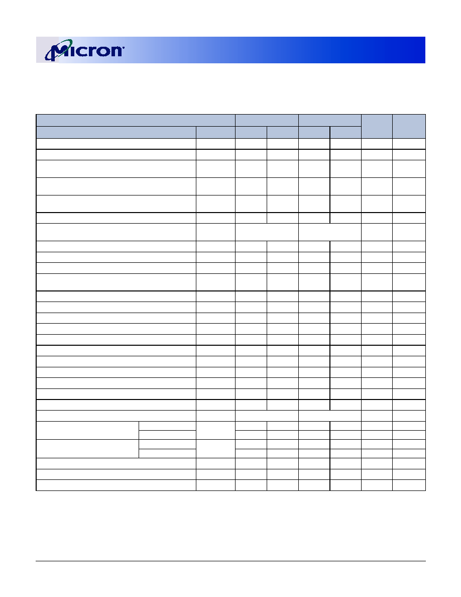
128MB, 256MB, 512MB, 1GB (x72, ECC, PLL)
200-PIN DDR SDRAM SODIMM
09005aef808ffdc7
Micron Technology, Inc., reserves the right to change products or specifications without notice.
DD9_18C16_32_64_128X72PHG_E.fm - Rev. E 7/03 EN
23
�2003 Micron Technology, Inc. All rights reserved.
Data-out high-impedance window from CK/CK#
t
HZ
+0.75
+0.8
ns
16, 37
Data-out low-impedance window from CK/CK#
t
LZ
-0.75
-0.8
ns
16, 38
Address and control input hold time (slow slew
rate)
t
IH
S
1.1
1.1
ns
12
Address and control input setup time (slow slew
rate)
t
IS
S
1.1
1.1
ns
12
Address and Control input pulse width (for each
input)
t
IPW
2.2
2.2
ns
LOAD MODE REGISTER command cycle time
t
MRD
15
16
ns
DQ-DQS hold, DQS to first DQ to go non-valid, per
access
t
QH
t
HP-
t
QHS
t
HP-
t
QHS
ns
22, 23
Data Hold Skew Factor
t
QHS
0.75
1
ns
ACTIVE to PRECHARGE command
t
RAS
40
120,000
40
120,000
ns
31
ACTIVE to READ with Auto precharge command
t
RAP
20
20
ns
ACTIVE to ACTIVE/AUTO REFRESH command
period
t
RC
65
70
ns
AUTO REFRESH command period
t
RFC
75
80
ns
44
ACTIVE to READ or WRITE delay
t
RCD
20
20
ns
PRECHARGE command period
t
RP
20
20
ns
DQS read preamble
t
RPRE
0.9
1.1
0.9
1.1
t
CK
37
DQS read postamble
t
RPST
0.4
0.6
0.4
0.6
t
CK
ACTIVE bank a to ACTIVE bank b command
t
RRD
15
15
ns
DQS write preamble
t
WPRE
0.25
0.25
t
CK
DQS write preamble setup time
t
WPRES
0
0
ns
18, 19
DQS write postamble
t
WPST
0.4
0.6
0.4
0.6
t
CK
17
Write recovery time
t
WR
15
15
ns
Internal WRITE to READ command delay
t
WTR
1
1
t
CK
Data valid output window (DVW)
na
t
QH -
t
DQSQ
t
QH -
t
DQSQ
ns
22
REFRESH to REFRESH command
interval
MT9VDDT1672PH
t
REFC
140.6
140.6
�s
21
All others
70.3
70.3
�s
21
Average periodic refresh
interval
MT9VDDT1672PH
t
REFI
15.6
15.6
�s
21
All others
0
7.8
7.8
�s
Terminating voltage delay to V
DD
t
VTD
0
0
ns
Exit SELF REFRESH to non-READ command
t
XSNR
75
75
ns
Exit SELF REFRESH to READ command
t
XSRD
200
200
t
CK
Table 21: Electrical Characteristics and Recommended AC Operating Conditions
(-26A, -265, and -202) (Continued)
DDR SDRAM components only; notes appear on pages 24�27
Notes: 1�5, 8, 12�15, 29, 48; 0
�C � T
A
� +70�C; V
DD
= V
DD
Q = +2.5V �0.2V
AC CHARACTERISTICS
-26A/-265
-202
UNITS
NOTES
PARAMETER
SYMBOL
MIN
MAX
MIN
MAX

128MB, 256MB, 512MB, 1GB (x72, ECC, PLL)
200-PIN DDR SDRAM SODIMM
09005aef808ffdc7
Micron Technology, Inc., reserves the right to change products or specifications without notice.
DD9_18C16_32_64_128X72PHG_E.fm - Rev. E 7/03 EN
24
�2003 Micron Technology, Inc. All rights reserved.
Notes
1. All voltages referenced to V
SS
.
2. Tests for AC timing, I
DD
, and electrical AC and DC
characteristics may be conducted at nominal ref-
erence/supply voltage levels, but the related spec-
ifications and device operation are guaranteed for
the full voltage range specified.
3. Outputs measured with equivalent load:
4. AC timing and I
DD
tests may use a V
IL
-to-V
IH
swing of up to 1.5V in the test environment, but
input timing is still referenced to V
REF
(or to the
crossing point for CK/CK#), and parameter speci-
fications are guaranteed for the specified AC input
levels under normal use conditions. The mini-
mum slew rate for the input signals used to test
the device is 1V/ns in the range between V
IL
(
AC
)
and V
IH
(
AC
).
5. The AC and DC input level specifications are as
defined in the SSTL_2 Standard (i.e., the receiver
will effectively switch as a result of the signal
crossing the AC input level, and will remain in that
state as long as the signal does not ring back
above [below] the DC input LOW [HIGH] level).
6. V
REF
is expected to equal V
DD
Q/2 of the transmit-
ting device and to track variations in the DC level
of the same. Peak-to-peak noise (non-common
mode) on Vref may not exceed �2 percent of the
DC value. Thus, from V
DD
Q/2, Vref is allowed
�25mV for DC error and an additional �25mV for
AC noise. This measurement is to be taken at the
nearest V
REF
bypass capacitor.
7. V
TT
is not applied directly to the device. V
TT
is a
system supply for signal termination resistors, is
expected to be set equal to V
REF
and must track
variations in the DC level of V
REF
.
8. I
DD
is dependent on output loading and cycle
rates. Specified values are obtained with mini-
mum cycle time at CL = 2 for -26A and -202, CL =
2.5 for -335 and -265 with the outputs open.
9. Enables on-chip refresh and address counters.
10. I
DD
specifications are tested after the device is
properly initialized, and is averaged at the defined
cycle rate.
11. This parameter is sampled. V
DD
=
+2.5V �0.2V
,
V
DD
Q =
+2.5V �0.2V
, V
REF
= V
SS
, f = 100 MHz, T
A
=
25�C, V
OUT
(
DC
) = V
DD
Q/2, V
OUT
(peak to peak) =
0.2V. DM input is grouped with I/O pins, reflecting
the fact that they are matched in loading.
12. Command/Address input slew rate = 0.5V/ns. For
-262, -26A and -265 with slew rates 1V/ns and
faster,
t
IS and
t
IH are reduced to 900ps; For -335
with slew rates 1 V/ns and faster,
t
IS and
t
IH are
reduced to 750ps. If the slew rate is less than 0.5V/
ns, timing must be derated:
t
IS has an additional
50ps per each 100 mV/ns reduction in slew rate
from the 500 mV /ns, while
t
IH remains constant.
If the slew rate exceeds 4.5V/ns, functionality is
uncertain.
13. The CK/CK# input reference level (for timing ref-
erenced to CK/CK#) is the point at which CK and
CK# cross; the input reference level for signals
other than CK/CK# is V
REF
.
14. Inputs are not recognized as valid until V
REF
stabi-
lizes. Exception: during the period before V
REF
stabilizes, CKE
� 0.3 x V
DD
Q is recognized as LOW.
15. The output timing reference level, as measured at
the timing reference point indicated in Note 3, is
V
TT
.
16.
t
HZ and
t
LZ transitions occur in the same access
time windows as data valid transitions. These
parameters are not referenced to a specific voltage
level, but specify when the device output is no
longer driving (HZ) or begins driving (LZ).
17. The intent of the Don't Care state after completion
of the postamble is the DQS-driven signal should
either be high, low, or high-Z and that any signal
transition within the input switching region must
follow valid input requirements. That is, if DQS
transitions high [above V
IHDC
(MIN)] then it must
not transition low (below V
IHDC
) prior to
t
DQSH
(MIN).
18. This is not a device limit. The device will operate
with a negative value, but system performance
could be degraded due to bus turnaround.
19. It is recommended that DQS be valid (HIGH or
LOW) on or before the WRITE command. The
case shown (DQS going from High-Z to logic
LOW) applies when no WRITEs were previously in
progress on the bus. If a previous WRITE was in
progress, DQS could be HIGH during this time,
depending on
t
DQSS.
20. MIN (
t
RC or
t
RFC) for I
DD
measurements is the
smallest multiple of
t
CK that meets the minimum
absolute value for the respective parameter.
t
RAS
(MAX) for I
DD
measurements is the largest multi-
Output
(V
OUT
)
Reference
Point
50
V
TT
30pF
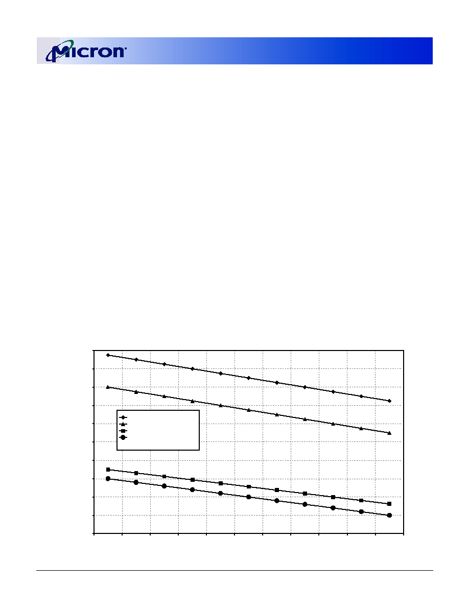
128MB, 256MB, 512MB, 1GB (x72, ECC, PLL)
200-PIN DDR SDRAM SODIMM
09005aef808ffdc7
Micron Technology, Inc., reserves the right to change products or specifications without notice.
DD9_18C16_32_64_128X72PHG_E.fm - Rev. E 7/03 EN
25
�2003 Micron Technology, Inc. All rights reserved.
ple of
t
CK that meets the maximum absolute
value for
t
RAS.
21. The refresh period 64ms. This equates to an aver-
age refresh rate of 15.625�s (MT9VDDT1672PH),
or 7.8251�s (MT9VDDT3272PH, MT18VDDT6472PH,
MT9VDDT6472PH, and MT18VDDT12872PH).
However, an AUTO REFRESH command must be
asserted at least once every 140.6�s
(MT9VDDT1672PH) or 70.3�s (MT9VDDT3272PH,
MT18VDDT6472PH, MT9VDDT6472PH, and
MT18VDDT12872PH); burst refreshing or posting
by the DRAM controller greater than eight refresh
cycles is not allowed.
22. The valid data window is derived by achieving
other specifications:
t
HP (
t
CK/2),
t
DQSQ, and
t
QH
(
t
QH =
t
HP -
t
QHS). The data valid window derates
in direct porportion with the clock duty cycle and
a practical data valid window can be derived, as
shown in Figure 8, Derating Data Valid Window.
The clock is allowed a maximum duty cycle varia-
tion of 45/55 beyond which functionality is uncer-
tain. The data valid window derating curves are
provided below for duty cycles ranging between
50/50 and 45/55.
23. Each byte lane has a corresponding DQS.
24. This limit is actually a nominal value and does not
result in a fail value. CKE is HIGH during
REFRESH command period (
t
RFC [MIN]) else
CKE is LOW (i.e., during standby).
25. To maintain a valid level, the transitioning edge of
the input must:
a. Sustain a constant slew rate from the current
AC level through to the target AC level, V
IL
(
AC
)
or V
IH
(
AC
).
b. Reach at least the target AC level.
c. After the AC target level is reached, continue to
maintain at least the target DC level, V
IL
(
DC
) or
V
IH
(
DC
).
26. JEDEC specifies CK and CK# input slew rate must
be
� 1V/ns (2V/ns differentially).
27. DQ and DM input slew rates must not deviate
from DQS by more than 10 percent. If the DQ/DM/
DQS slew rate is less than 0.5V/ns, timing must be
derated: 50ps must be added to
t
DS and
t
DH for
each 100mv/ns reduction in slew rate. If slew rate
exceeds 4V/ns, functionality is uncertain.
28. V
DD
must not vary more than 4 percent if CKE is
not active while any bank is active.
29. The clock is allowed up to �150ps of jitter. Each
timing parameter is allowed to vary by the same
amount.
Figure 8: Derating Data Valid Window
(
t
QH -
t
DQSQ)
3.750
3.700
3.650
3.600
3.550
3.500
3.450
3.400
3.350
3.300
3.250
3.400
3.350
3.300
3.250
3.200
3.150
3.100
3.050
3.000
2.950
2.900
2.500
2.463
2.425
2.388
2.350
2.313
2.275
2.238
2.200
2.163
2.125
1.8
2.0
2.2
2.4
2.6
2.8
3.0
3.2
3.4
3.6
3.8
50/50
49.5/50.5 49/51
48.5/52.5
48/52
47.5/53.5
47/53
46.5/54.5
46/54
45.5/55.5
45/55
Clock Duty Cycle
ns
-26A/-265 @
t
CK = 10ns
-202 @
t
CK = 10ns
-262/-26A/-265 @
t
CK = 7.5ns
-202 @
t
CK = 8ns
-335 @
t
CK = 6ns
N/A
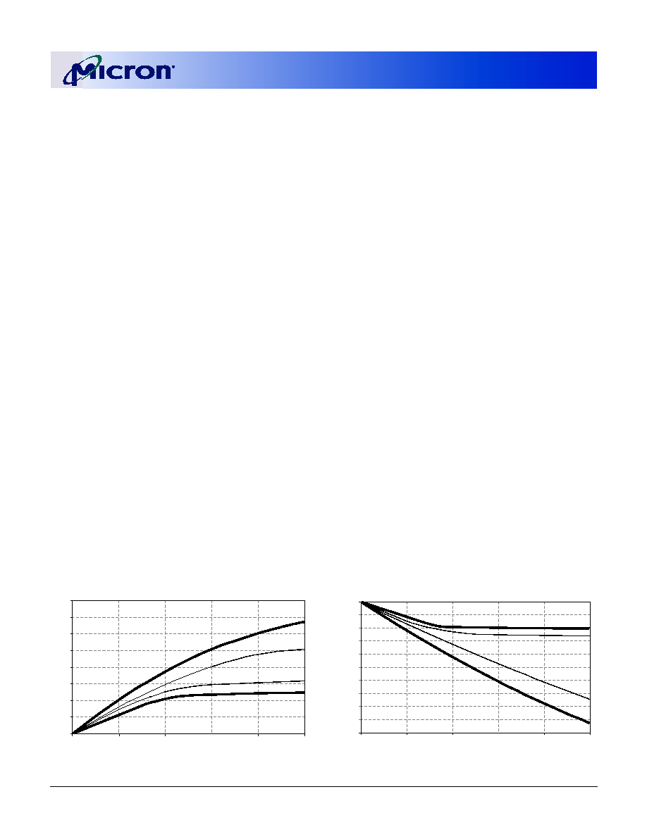
128MB, 256MB, 512MB, 1GB (x72, ECC, PLL)
200-PIN DDR SDRAM SODIMM
09005aef808ffdc7
Micron Technology, Inc., reserves the right to change products or specifications without notice.
DD9_18C16_32_64_128X72PHG_E.fm - Rev. E 7/03 EN
26
�2003 Micron Technology, Inc. All rights reserved.
30.
t
HP min is the lesser of
t
CL minimum and t
t
CH
minimum actually applied to the device CK and
CK# inputs, collectively during bank active.
31. READs and WRITEs with auto precharge are not
allowed to be issued until
t
RAS(min) can be satis-
fied prior to the internal precharge command
being issued.
32. Any positive glitch must be less than 1/3 of the
clock and not more than +400mV or 2.9V, which-
ever is less. Any negative glitch must be less than
1/3 of the clock cycle and not exceed either -
300mV or 2.2V, whichever is more positive.
33. Normal Output Drive Curves:
a. The full variation in driver pull-down current
from minimum to maximum process, temper-
ature and voltage will lie within the outer
bounding lines of the V-I curve of Figure 9,
Pull-Down Characteristics.
b. The variation in driver pull-down current within
nominal limits of voltage and temperature is
expected, but not guaranteed, to lie within the
inner bounding lines of the V-I curve of Figure 9,
Pull-Down Characteristics.
c. The full variation in driver pull-up current from
minimum to maximum process, temperature
and voltage will lie within the outer bounding
lines of the V-I curve of Figure 10, Pull-Up Char-
acteristics
d. The variation in driver pull-up current within
nominal limits of voltage and temperature is
expected, but not guaranteed, to lie within the
inner bounding lines of the V-I curve of Figure
10, Pull-Up Characteristics.
e. The full variation in the ratio of the maximum to
minimum pull-up and pull-down current
should be between 0.71 and 1.4, for device
drain-to-source voltages from 0.1V to 1.0V, and
at the same voltage and temperature.
f. The full variation in the ratio of the nominal
pull-up to pull-down current should be unity
�10 percent, for device drain-to-source voltages
from 0.1V to 1.0V.
34. The voltage levels used are derived from a mini-
mum V
DD
level and the referenced test load. In
practice, the voltage levels obtained from a prop-
erly terminated bus will provide significantly dif-
ferent voltage values.
35. V
IH
overshoot: V
IH
(MAX) = V
DD
Q + 1.5V for a
pulse width
� 3ns and the pulse width can not be
greater than 1/3 of the cycle rate. V
IL
undershoot:
V
IL
(MIN) = -1.5V for a pulse width
� 3ns and the
pulse width can not be greater than 1/3 of the
cycle rate.
36. V
DD
and V
DD
Q must track each other.
37. This maximum value is derived from the refer-
enced test load. In practice, the values obtained
in a typical terminated design may reflect up to
310ps less for
t
HZ(MAX) and the last DVW.
t
HZ(MAX) will prevail over
t
DQSCK(MAX) +
t
RPST(MAX) condition.
t
LZ(MIN) will prevail over
t
DQSCK(MIN) +
t
RPRE(MAX) condition.
38. For slew rates greater than 1V/ns the (LZ) transi-
tion will start about 310ps earlier.
39. During initialization, V
DD
Q, V
TT
, and V
REF
must
be equal to or less than V
DD
+ 0.3V. Alternatively,
V
TT
may be 1.35V maximum during power up,
even if V
DD
/V
DD
Q are 0Vs, provided a minimum
of 42
W of series resistance is used between the V
TT
supply and the input pin.
40. The current Micron part operates below the slow-
est JEDEC operating frequency of 83 MHz. As
such, future die may not reflect this option.
Figure 9: Pull-Down Characteristics
Figure 10: Pull-Up Characteristics
160
140
I
OUT
(mA)
V
OUT
(V)
Nominal low
Minimum
Nominal high
Maximum
120
100
80
60
40
20
0
0.0
0.5
1.0
1.5
2.0
2.5
V
OUT
(V)
0
-20
I
OUT
(mA)
Nominal low
Minimum
Nominal high
Maximum
-40
-60
-80
-100
-120
-140
-160
-180
-200
0.0
0.5
1.0
1.5
2.0
2.5
V
DD
Q - V
OUT
(V)

128MB, 256MB, 512MB, 1GB (x72, ECC, PLL)
200-PIN DDR SDRAM SODIMM
09005aef808ffdc7
Micron Technology, Inc., reserves the right to change products or specifications without notice.
DD9_18C16_32_64_128X72PHG_E.fm - Rev. E 7/03 EN
27
�2003 Micron Technology, Inc. All rights reserved.
41. For -335, -262, -26A, -265, and -202 modules,
I
DD
3N is specified to be 35mA per DDR SDRAM
device at 100 MHz.
42. Random addressing changing and 50 percent of
data changing at every transfer.
43. Random addressing changing and 100 percent of
data changing at every transfer.
44. CKE must be active (high) during the entire time a
refresh command is executed. That is, from the
time the AUTO REFRESH command is registered,
CKE must be active at each rising clock edge, until
t
REF later.
45. I
DD
2N specifies the DQ, DQS, and DM to be
driven to a valid high or low logic level. I
DD
2Q is
similar to I
DD
2F except I
DD
2Q specifies the
address and control inputs to remain stable.
Although I
DD
2F, I
DD
2N, and I
DD
2Q are similar,
I
DD
2F is "worst case."
46. Whenever the operating frequency is altered, not
including jitter, the DLL is required to be reset.
This is followed by 200 clock cycles.
47. Leakage number reflects the worst case leakage
possible through the module pin, not what each
memory device contributes.
48. When an input signal is HIGH or LOW, it is
defined as a steady state logic HIGH or LOW.
128MB, 256MB, 512MB, 1GB (x72, ECC, PLL)
200-PIN DDR SDRAM SODIMM
09005aef808ffdc7
Micron Technology, Inc., reserves the right to change products or specifications without notice.
DD9_18C16_32_64_128X72PHG_E.fm - Rev. E 7/03 EN
28
�2003 Micron Technology, Inc. All rights reserved.
NOTE:
1. The timing and switching specifications for the PLL listed above are critical for proper operation of the DDR SDRAM
Registered DIMMs. These are meant to be a subset of the parameters for the specific device used on the module.
Detailed information for this PLL is available in JEDEC Standard JESD82.
2. The PLL must be able to handle spread spectrum induced skew.
3. Operating clock frequency indicates a range over which the PLL must be able to lock, but in which it is not required
to meet the other timing parameters. (Used for low-speed system debug.)
4. Stabilization time is the time required for the integrated PLL circuit to obtain phase lock of its feedback signal to its
reference signal after power up.
5. Static Phase Offset does not include Jitter.
6. Period Jitter and Half-Period Jitter specifications are separate specifications that must be met independently of each
other.
7. The Output Slew Rate is determined from the IBIS model:
Table 22: PLL Clock Driver Timing Requirements and Switching Characteristics
Note: 1
PARAMETER
SYMBOL
0�C
� T
A
� 70�C
V
DD
= 2.5V � 0.2V
UNITS
NOTES
MIN
NOMINAL
MAX
Operating Clock Frequency
f
CK
60
-
170
MHz
2, 3
Input Duty Cycle
t
DC
40
-
60
%
Stabilization Time
t
STAB
-
-
100
ms
4
Cycle to Cycle Jitter
t
JIT
CC
-75
-
75
ps
Static Phase Offset
t
�
-50
0
50
ps
5
Output Clock Skew
t
SK
O
-
-
100
ps
Period Jitter
t
JIT
PER
-75
-
75
ps
6
Half-Period Jitter
t
JIT
HPER
-100
-
100
ps
6
Input Clock Slew Rate
t
LS
I
1.0
-
4
V/ns
Output Clock Slew Rate
t
LS
O
1.0
-
2
V/ns
7
V
DD
/2
GND
V
DD
CDCV857
R=60
R=60
V
CK
V
CK
128MB, 256MB, 512MB, 1GB (x72, ECC, PLL)
200-PIN DDR SDRAM SODIMM
09005aef808ffdc7
Micron Technology, Inc., reserves the right to change products or specifications without notice.
DD9_18C16_32_64_128X72PHG_E.fm - Rev. E 7/03 EN
29
�2003 Micron Technology, Inc. All rights reserved.
SPD Clock and Data Conventions
Data states on the SDA line can change only during
SCL LOW. SDA state changes during SCL HIGH are
reserved for indicating start and stop conditions (as
shown in Figure 11, Data Validity, and Figure 12, Defi-
nition of Start and Stop).
SPD Start Condition
All commands are preceded by the start condition,
which is a HIGH-to-LOW transition of SDA when SCL
is HIGH. The SPD device continuously monitors the
SDA and SCL lines for the start condition and will not
respond to any command until this condition has been
met.
SPD Stop Condition
All communications are terminated by a stop condi-
tion, which is a LOW-to-HIGH transition of SDA when
SCL is HIGH. The stop condition is also used to place
the SPD device into standby power mode.
SPD Acknowledge
Acknowledge is a software convention used to indi-
cate successful data transfers. The transmitting device,
either master or slave, will release the bus after trans-
mitting eight bits. During the ninth clock cycle, the
receiver will pull the SDA line LOW to acknowledge
that it received the eight bits of data (as shown in Fig-
ure 13, Acknowledge Response from Receiver).
The SPD device will always respond with an
acknowledge after recognition of a start condition and
its slave address. If both the device and a WRITE oper-
ation have been selected, the SPD device will respond
with an acknowledge after the receipt of each subse-
quent eight-bit word. In the read mode the SPD device
will transmit eight bits of data, release the SDA line and
monitor the line for an acknowledge. If an acknowl-
edge is detected and no stop condition is generated by
the master, the slave will continue to transmit data. If
an acknowledge is not detected, the slave will termi-
nate further data transmissions and await the stop
condition to return to standby power mode.
Figure 11: Data Validity
Figure 12: Definition of Start and Stop
Figure 13: Acknowledge Response from Receiver
SCL
SDA
DATA STABLE
DATA STABLE
DATA
CHANGE
SCL
SDA
START
BIT
STOP
BIT
SCL from Master
Data Output
from Transmitter
Data Output
from Receiver
9
8
Acknowledge

128MB, 256MB, 512MB, 1GB (x72, ECC, PLL)
200-PIN DDR SDRAM SODIMM
09005aef808ffdc7
Micron Technology, Inc., reserves the right to change products or specifications without notice.
DD9_18C16_32_64_128X72PHG_E.fm - Rev. E 7/03 EN
30
�2003 Micron Technology, Inc. All rights reserved.
Figure 14: SPD EEPROM Timing Diagram
Table 23: EEPROM Device Select Code
Most significant bit (b7) is sent first
SELECT CODE
DEVICE TYPE IDENTIFIER
CHIP ENABLE
RW
b7
b6
b5
b4
b3
b2
b1
b0
Memory Area Select Code (two arrays)
1
0
1
0
SA2
SA1
SA0
RW
Protection Register Select Code
0
1
1
0
SA2
SA1
SA0
RW
Table 24: EEPROM Operating Modes
MODE
RW BIT
WC
BYTES
INITIAL SEQUENCE
Current Address Read
1
V
IH
or V
IL
1
START, Device Select, RW = `1'
Random Address Read
0
V
IH
or V
IL
1
START, Device Select, RW = `0', Address
1
V
IH
or V
IL
1
reSTART, Device Select, RW = `1'
Sequential Read
1
V
IH
or V
IL
� 1
Similar to Current or Random Address Read
Byte Write
0
V
IL
1
START, Device Select, RW = `0'
Page Write
0
V
IL
� 16
START, Device Select, RW = `0'
SCL
SDA IN
SDA OUT
tLOW
tSU:STA
tHD:STA
tF
tHIGH
tR
tBUF
tDH
tAA
tSU:STO
tSU:DAT
tHD:DAT
UNDEFINED
128MB, 256MB, 512MB, 1GB (x72, ECC, PLL)
200-PIN DDR SDRAM SODIMM
09005aef808ffdc7
Micron Technology, Inc., reserves the right to change products or specifications without notice.
DD9_18C16_32_64_128X72PHG_E.fm - Rev. E 7/03 EN
31
�2003 Micron Technology, Inc. All rights reserved.
NOTE:
1. To avoid spurious START and STOP conditions, a minimum delay is placed between SCL = 1 and the falling or rising
edge of SDA.
2. This parameter is sampled.
3. For a reSTART condition, or following a WRITE cycle.
4. The SPD EEPROM WRITE cycle time (
t
WRC) is the time from a valid stop condition of a write sequence to the end of
the EEPROM internal erase/program cycle. During the WRITE cycle, the EEPROM bus interface circuit is disabled, SDA
remains HIGH due to pull-up resistor, and the EEPROM does not respond to its slave address.
Table 25: Serial Presence-Detect EEPROM DC Operating Conditions
All voltages referenced to V
SS
; V
DDSPD
= +2.3V to +3.6V
PARAMETER/CONDITION
SYMBOL
MIN
MAX
UNITS
SUPPLY VOLTAGE
V
DD
2.3
3.6
V
INPUT HIGH VOLTAGE: Logic 1; All inputs
V
IH
V
DD
X
0.7
V
DD
+ 0.5
V
INPUT LOW VOLTAGE: Logic 0; All inputs
V
IL
-1
V
DD
x 0.3
V
OUTPUT LOW VOLTAGE: I
OUT
= 3mA
V
OL
�
0.4
V
INPUT LEAKAGE CURRENT: V
IN
= GND to V
DD
I
LI
�
10
�A
OUTPUT LEAKAGE CURRENT: V
OUT
= GND to V
DD
I
LO
�
10
�A
STANDBY CURRENT:
SCL = SDA = V
DD
- 0.3V; All other inputs = V
SS
or V
DD
I
SB
�
30
�A
POWER SUPPLY CURRENT: SCL clock frequency = 100 KHz
I
DD
�
2
mA
Table 26: Serial Presence-Detect EEPROM AC Operating Conditions
All voltages referenced to V
SS
; V
DDSPD
= +2.3V to +3.6V
PARAMETER/CONDITION
SYMBOL
MIN
MAX
UNITS
NOTES
SCL LOW to SDA data-out valid
t
AA
0.2
0.9
�s
1
Time the bus must be free before a new transition can start
t
BUF
1.3
�s
Data-out hold time
t
DH
200
ns
SDA and SCL fall time
t
F
300
ns
2
Data-in hold time
t
HD:DAT
0
�s
Start condition hold time
t
HD:STA
0.6
�s
Clock HIGH period
t
HIGH
0.6
�s
Noise suppression time constant at SCL, SDA inputs
t
I
50
ns
Clock LOW period
t
LOW
1.3
�s
SDA and SCL rise time
t
R
0.3
�s
2
SCL clock frequency
f
SCL
400
KHz
Data-in setup time
t
SU:DAT
100
ns
Start condition setup time
t
SU:STA
0.6
�s
3
Stop condition setup time
t
SU:STO
0.6
�s
WRITE cycle time
t
WRC
10
ms
4

128MB, 256MB, 512MB, 1GB (x72, ECC, PLL)
200-PIN DDR SDRAM SODIMM
09005aef808ffdc7
Micron Technology, Inc., reserves the right to change products or specifications without notice.
DD9_18C16_32_64_128X72PHG_E.fm - Rev. E 7/03 EN
32
�2003 Micron Technology, Inc. All rights reserved.
Table 27: Serial Presence-Detect Matrix (MT9VDDT1672PH, MT9VDDT3272PH, and
MT9VDDT6472PH)
"1"/"0": Serial Data, "driven to HIGH"/"driven to LOW"
BYTE
DESCRIPTION
ENTRY(VERSION) MT9VDDT1672PH MT9VDDT3272PH MT9VDDT6472PH
0
Number of SPD Bytes Used by Micron
128
80
80
80
1
Total Number of Bytes in SPD Device
256
08
08
08
2
Fundamental Memory Type
DDR SDRAM
07
07
07
3
Number of Row Addresses on Assembly
12 or13
0C
0D
0D
4
Number of Column Addresses on
Assembly
10
0A
0A
0B
5
Number of Physical Ranks on DIMM
1
01
01
01
6
Module Data Width
72
48
48
48
7
Module Data Width (Continued)
0
00
00
00
8
Module Voltage Interface Levels
SSTL 2.5V
04
04
04
9
SDRAM Cycle Time,
t
CK (CAS Latency =
2.5)
(See note 1)
6ns (-335)
7ns (-262/-26A)
7.5ns (-265)
8ns (-202)
60
70
75
80
60
70
75
80
60
70
75
80
10
SDRAM Access from Clock,
t
AC (CAS
Latency = 2.5)
(See note 1)
0.7ns (-335)
0.75ns (-262/-26A/-
265)
0.8ns (-202)
70
75
80
70
75
80
70
75
80
11
Module Configuration Type
ECC
02
02
02
12
Refresh Rate/ Type
15.6�s or 7.8�s/SELF
80
82
82
13
SDRAM Device Width (Primary DDR
SDRAM)
8
08
08
08
14
Error-checking DDR SDRAM Data Width
8
08
08
08
15
Minimum Clock Delay, Back-to-Back
Random Column Access
1 clock
01
01
01
16
Burst Lengths Supported
2, 4, 8
0E
0E
0E
17
Number of Banks on DDR SDRAM
Device
4
04
04
04
18
CAS Latencies Supported
2, 2.5
0C
0C
0C
19
CS Latency
0
01
01
01
20
WE Latency
1
02
02
02
21
SDRAM Module Attributes
Unbuffered, Diff
CLK, PLL
24
24
24
22
SDRAM Device Attributes: General
Fast/concurrent
auto precharge
00
C0
C0
23
SDRAM Cycle Time,
t
CK (CAS Latency =
2) (See note 2)
7.5ns (-335/-262/-26A)
10ns (-202/-265)
75
A0
75
A0
75
A0
24
SDRAM Access from CK,
t
AC (CAS
Latency = 2) (See note 2)
0.7ns (-335)
0.75ns (-265/-26A)
0.8ns (-202)
70
75
80
70
75
80
70
75
80
25
SDRAM Cycle Time,
t
CK (CAS Latency =
1.5)
N/A
00
00
00
26
SDRAM Access from CK,
t
AC (CAS
Latency = 1.5)
N/A
00
00
00
128MB, 256MB, 512MB, 1GB (x72, ECC, PLL)
200-PIN DDR SDRAM SODIMM
09005aef808ffdc7
Micron Technology, Inc., reserves the right to change products or specifications without notice.
DD9_18C16_32_64_128X72PHG_E.fm - Rev. E 7/03 EN
33
�2003 Micron Technology, Inc. All rights reserved.
27
Minimum Row Precharge Time,
t
RP
18ns (-335)
15ns (-262)
20ns (-26A/-265/-202)
48
3C
50
48
3C
50
48
3C
50
28
Minimum Row Active to Row Active,
t
RRD
12ns (-335)
15ns (-262/-26A/-265/-202)
30
3C
30
3C
30
3C
29
Minimum RAS# to CAS# Delay,
t
RCD
18ns (-335)
15ns (-262)
20ns (-26A/-265/-202)
48
3C
50
48
3C
50
48
3C
50
30
Minimum RAS# Pulse Width,
t
RAS (See
note 3)
42ns (-335)
45ns (-262/-26A/-265)
40ns (-202)
2A
2D
28
2A
2D
28
2A
2D
28
31
Module Rank Density
128MB or 256MB
20
40
80
32
Address and Command Setup Time,
t
IS
(see note 4)
0.8ns (-335)
1.0ns (-262/-26A/-265)
1.1ns (-202)
80
A0
B0
80
A0
B0
80
A0
B0
33
Address and Command Hold Time,
t
IH
(see note 4)
0.8ns (-335)
1.0ns (-262/-26A/-265)
1.1ns (-202)
80
A0
B0
80
A0
B0
80
A0
B0
34
Data/Data Mask Input Setup Time,
t
DS
0.45ns (-335
0.5ns (-262/-26A/-265)
0.6ns (-202)
45
50
60
45
50
60
45
50
60
35
Data/ Data Mask Input Hold Time,
t
DH
0.45ns (-335
0.5ns (-262/-26A/-265)
0.6ns (-202)
45
50
60
45
50
60
45
50
60
36-40 Reserved
00
00
00
41
Min Active Refresh Time
t
RC
60ns (-335/-262)
65ns (-26A/-265)
70ns (-202)
3C
41
46
3C
41
46
3C
41
46
42
Minimum Auto Refresh to Active/Auto
Refresh Command Period,
t
RFC
72ns (-335)
75ns (-262/-26A/-265)
80ns (-202)
48
4B
50
48
4B
50
48
4B
50
43
SDRAM Device Max Cycle Time,
t
CK
MAX
12ns (-335)
13ns (-262/-26A/-265/-202)
30
34
30
34
30
34
44
SDRAM Device Max DQS-DQ Skew Time,
t
DQSQ
0.45ns (-335)
0.5ns (-262/-26A/-265)
0.6ns (-202)
2D
32
3C
2D
32
3C
2D
32
3C
45
SDRAM Device Max Read Data Hold
Skew Factor
0.6ns (-335)
0.75ns (-262/-26A/-265)
1ns (-202)
55
75
A0
55
75
A0
55
75
A0
46
Reserved
00
00
00
47
DIMM Height
11/01
11/01
11/01
48�61 Reserved
00
00
00
62
SPD Revision
Initial Release 0.0
10
10
10
63
Checksum For Bytes 0-62
-335
-262
-26A
-265
-202
2A/1A (see note 5)
FD/ED (see note 5)
2A/1A (see note 5)
5A/4A (see note 5)
F5/E5 (see note 5)
4D/3D (see note 5)
E0/D0 (see note 5)
0D/FD (see note 5)
3D/2D (see note 5)
D8/C8 (see note 5)
8E/7E (see note 5)
21/11 (see note 5)
4E/3E (see note 5)
80/6E (see note 5)
19/09 (see note 5)
Table 27: Serial Presence-Detect Matrix (MT9VDDT1672PH, MT9VDDT3272PH, and
MT9VDDT6472PH) (Continued)
"1"/"0": Serial Data, "driven to HIGH"/"driven to LOW"
BYTE
DESCRIPTION
ENTRY(VERSION) MT9VDDT1672PH MT9VDDT3272PH MT9VDDT6472PH

128MB, 256MB, 512MB, 1GB (x72, ECC, PLL)
200-PIN DDR SDRAM SODIMM
09005aef808ffdc7
Micron Technology, Inc., reserves the right to change products or specifications without notice.
DD9_18C16_32_64_128X72PHG_E.fm - Rev. E 7/03 EN
34
�2003 Micron Technology, Inc. All rights reserved.
NOTE:
1. Device latencies used for SPD values.
2. Value for -262/-26A
t
CK set to 7ns (0x70) for optimum BIOS compatibility. Actual device spec. value is 7.5ns.
3. The value of
t
RAS used for -265 modules is calculated from
t
RC -
t
RP. Actual device spec value is 40ns.
4. The JEDEC SPD specification allows fast or slow slew rate values for these bytes. The worst-case (slow slew rate) value is
represented here. Systems requiring the fast slew rate setup and hold values are supported, provided the faster mini-
mum slew rate is met.
5. Values given in format "standard DIMM Height checksum / low-profile DIMM height checksum."
64
Manufacturer's JEDEC ID Code
MICRON
2C
2C
2C
65-71 Manufacturer's JEDEC ID Code
(continued)
00
00
00
72
Manufacturing Location
01�12
01�0C
01�0C
01�0C
73-90 Module Part Number (ASCII)
Variable Data
Variable Data
Variable Data
91
PCB Identification Code
1�9
01�09
01�09
01�09
92
Identification Code (Continued)
0
00
00
00
93
Year Of Manufacture in BCD
Variable Data
Variable Data
Variable Data
94
Week Of Manufacture in BCD
Variable Data
Variable Data
Variable Data
95-98 Module Serial Number
Variable Data
Variable Data
Variable Data
99-
127
Manufacturer-Specific Data ( RSVD)
�
�
�
Table 27: Serial Presence-Detect Matrix (MT9VDDT1672PH, MT9VDDT3272PH, and
MT9VDDT6472PH) (Continued)
"1"/"0": Serial Data, "driven to HIGH"/"driven to LOW"
BYTE
DESCRIPTION
ENTRY(VERSION) MT9VDDT1672PH MT9VDDT3272PH MT9VDDT6472PH

128MB, 256MB, 512MB, 1GB (x72, ECC, PLL)
200-PIN DDR SDRAM SODIMM
09005aef808ffdc7
Micron Technology, Inc., reserves the right to change products or specifications without notice.
DD9_18C16_32_64_128X72PHG_E.fm - Rev. E 7/03 EN
35
�2003 Micron Technology, Inc. All rights reserved.
Table 28: Serial Presence- Detect Matrix (MT18VDDT6472PH
and
MT18VDDT12872PH)
"1"/"0": Serial Data, "driven to HIGH"/"driven to LOW"
BYTE
DESCRIPTION
ENTRY(VERSION)
MT18VDDT6472PH MT18VDDT12872PH
0
Number of SPD Bytes Used by Micron
128
80
80
1
Total Number of Bytes in SPD Device
256
08
08
2
Fundamental Memory Type
SDRAM DDR
07
07
3
Number of Row Addresses on Assembly
13
0D
0D
4
Number of Column Addresses on Assembly
11
0A
0B
5
Number of Physical Ranks on DIMM
2
02
02
6
Module Data Width
72
48
48
7
Module Data Width (Continued)
0
00
00
8
Module Voltage Interface Levels
SSTL 2.5V
04
04
9
SDRAM Cycle Time,
t
CK (CAS Latency = 2.5)
(See note 1)
6ns (-335)
7ns (-262/-26A)
7.5ns (-265)
8ns (-202)
60
70
75
80
60
70
75
80
10
SDRAM Access from Clock,
t
AC (CAS Latency =
2.5)
(See note 1)
0.7ns (-335)
0.75ns (-262/-26A/-265)
0.8ns (-202)
70
75
80
70
75
80
11
Module Configuration Type
ECC
02
02
12
Refresh Rate/ Type
7.8�s/SELF
82
82
13
SDRAM Device Width (Primary DDR SDRAM)
x8
08
08
14
Error-checking DDR SDRAM Data Width
x8
08
08
15
Minimum Clock Delay, Back-to-Back Random
Column Access
1 clock
01
01
16
Burst Lengths Supported
2, 4, 8
0E
0E
17
Number of Banks on DDR SDRAM Device
4
04
04
18
CAS Latencies Supported
2.5
0C
0C
19
CS Latency
0
01
01
20
WE Latency
1
02
02
21
SDRAM Module Attributes
Unbuffered, Diff CLK,
PLL
24
24
22
SDRAM Device Attributes: General
Fast/concurrent auto
precharge
C0
C0
23
SDRAM Cycle Time,
t
CK (CAS Latency = 2)
(See note 2)
7.5ns (-335/-26A/-262)
10ns (-265/-202)
75
A0
75
A0
24
SDRAM Access from CK,
t
AC (CAS Latency = 2)
(See note 2)
0.7ns (-335)
0.75ns (-262/-26A/-265)
0.8ns (-202)
70
75
80
70
75
80
25
SDRAM Cycle Time,
t
CK (CAS Latency = 1.5)
N/A
00
00
26
SDRAM Access from CK,
t
AC (CAS Latency = 1.5)
N/A
00
00
27
Minimum Row Precharge Time,
t
RP
18ns (-335)
15ns (-262)
20ns (-202/-265/-26A)
48
3C
50
48
3C
50
28
Minimum Row Active to Row Active,
t
RRD
12ns (-335)
15ns (-262/-26A/-265/-202)
30
3C
30
3C

128MB, 256MB, 512MB, 1GB (x72, ECC, PLL)
200-PIN DDR SDRAM SODIMM
09005aef808ffdc7
Micron Technology, Inc., reserves the right to change products or specifications without notice.
DD9_18C16_32_64_128X72PHG_E.fm - Rev. E 7/03 EN
36
�2003 Micron Technology, Inc. All rights reserved.
29
Minimum RAS# to CAS# Delay,
t
RCD
18ns (-335)
15ns (-262)
20ns (-26A/-265/-202)
48
3C
50
48
3C
50
30
Minimum RAS# Pulse Width,
t
RAS (See note 3)
42ns (-335)
45ns (-262/-26A/-265)
40ns (-202)
2A
2D
28
2A
2D
28
31
Module Rank Density
512MB
40
80
32
Address and Command Setup Time,
t
IS
(see note 4)
0.8ns (-335)
1.0ns (-262/-26A/-265)
1.1ns (-202)
80
A0
B0
80
A0
B0
33
Address and Command Hold Time,
t
IH
(see note 4)
0.8ns (-335)
1.0ns (-262/-26A/-265)
1.1ns (-202)
80
A0
B0
80
A0
B0
34
Data/Data Mask Input Setup Time,
t
DS
0.45ns (-335
0.5ns (-262/-26A/-265)
0.6ns (-202)
45
50
60
45
50
60
35
Data/ Data Mask Input Hold Time,
t
DH
0.45ns (-335
0.5ns (-262/-26A/-265)
0.6ns (-202)
45
50
60
45
50
60
36-40 Reserved
00
00
41
Min Active Refresh Time
t
RC
60ns (-335/-262)
65ns (-265/-26A)
70ns (-202)
3C
41
46
3C
41
46
42
Minimum Auto Refresh to Active/Auto
Refresh Command Period,
t
RFC
72ns (-335)
75ns (-262/-26A/-265)
80ns (-202)
48
4B
50
48
4B
50
43
SDRAM Device Max Cycle Time,
t
CK
MAX
12ns (-335)
13ns (-262/-26A/-265/-
202)
30
34
30
34
44
SDRAM Device Max DQS-DQ Skew Time,
t
DQSQ
0.45ns (-335)
0.5ns (-262/-26A/-265)
0.6ns (-202)
2D
32
3C
2D
32
3C
45
SDRAM Device Max Read Data Hold Skew
Factor
0.6ns (-335)
0.75ns (-262/-26A/-265)
1ns (-202)
55
75
A0
55
75
A0
46
Reserved
00
00
47
DIMM Height
Standard/Low Profile
11/01
11/01
48�61 Reserved
00
00
62
SPD Revision
Initial Release 0.0
10
10
63
Checksum For Bytes 0-62
-335
-262
-26A
-265
-202
4E/3E (see note 5)
E1/D1 (see note 5)
0E/FE (see note 5)
3E/2E (see note 5)
D9/C9 (see note 5)
8F/7F (see note 5)
2C/12 (see note 5)
4F/3F (see note 5)
7F/6F (see note 5)
1A/0A (see note 5)
64
Manufacturer's JEDEC ID Code
MICRON
2C
2C
65-71 Manufacturer's JEDEC ID Code (continued)
00
00
72
Manufacturing Location
01�12
01�0B
01�0C
73-90 Module Part Number (ASCII)
Variable Data
Variable Data
Table 28: Serial Presence- Detect Matrix (MT18VDDT6472PH
and
MT18VDDT12872PH) (Continued)
"1"/"0": Serial Data, "driven to HIGH"/"driven to LOW"
BYTE
DESCRIPTION
ENTRY(VERSION)
MT18VDDT6472PH MT18VDDT12872PH
128MB, 256MB, 512MB, 1GB (x72, ECC, PLL)
200-PIN DDR SDRAM SODIMM
09005aef808ffdc7
Micron Technology, Inc., reserves the right to change products or specifications without notice.
DD9_18C16_32_64_128X72PHG_E.fm - Rev. E 7/03 EN
37
�2003 Micron Technology, Inc. All rights reserved.
NOTE:
1. Device latencies used for SPD values.
2. Value for -26A
t
CK set to 7ns (0x70) for optimum BIOS compatibility. Actual device spec. value is 7.5ns.
3. The value of
t
RAS used for -265 modules is calculated from
t
RC -
t
RP. Actual device spec value is 40ns.
4. The JEDEC SPD specification allows fast or slow slew rate values for these bytes. The worst-case (slow slew rate) value is
represented here. Systems requiring the fast slew rate setup and hold values are supported, provided the faster mini-
mum slew rate is met.
5. Values given in format "standard DIMM Height checksum / low-profile DIMM height checksum."
91
PCB Identification Code
1�9
01�09
01�09
92
Identification Code (Continued)
0
00
00
93
Year of Manufacture in BCD
Variable Data
Variable Data
94
Week of Manufacture in BCD
Variable Data
Variable Data
95-98 Module Serial Number
Variable Data
Variable Data
99-127 Manufacturer-Specific Data ( RSVD)
�
�
Table 28: Serial Presence- Detect Matrix (MT18VDDT6472PH
and
MT18VDDT12872PH) (Continued)
"1"/"0": Serial Data, "driven to HIGH"/"driven to LOW"
BYTE
DESCRIPTION
ENTRY(VERSION)
MT18VDDT6472PH MT18VDDT12872PH
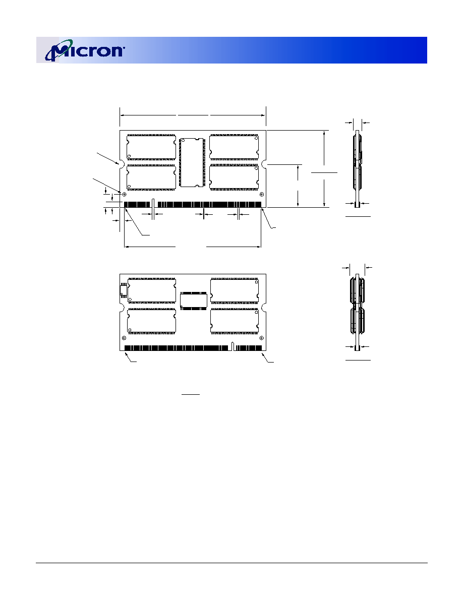
128MB, 256MB, 512MB, 1GB (x72, ECC, PLL)
200-PIN DDR SDRAM SODIMM
09005aef808ffdc7
Micron Technology, Inc., reserves the right to change products or specifications without notice.
DD9_18C16_32_64_128X72PHG_E.fm - Rev. E 7/03 EN
38
�2003 Micron Technology, Inc. All rights reserved.
Figure 15: Standard 200-Pin SODIMM Dimensions
NOTE:
All dimensions are in inches (millimeters),
, or typical where noted.
U1
U3
U9
U7
U5
U11
U8
U6
U10
U2
U4
0.150 (3.80)
MAX
0.043 (1.10)
0.035 (0.90)
PIN 1
2.666 (67.72)
2.656 (67.45)
0.787 (20.00)
TYP
0.071 (1.80)
(2X)
0.024 (0.61)
TYP
0.018 (0.46)
TYP
0.079 (2.00) R
(2X)
PIN 199
PIN 200
PIN 2
FRONT VIEW
0.079 (2.00)
0.236 (6.00)
2.504 (63.60)
0.096 (2.44)
0.039 (0.99)
TYP
1.405 (35.69)
1.395 (35.43)
BACK VIEW
0.320 (8.13)
MAX
Single Rank Modules
Dual Rank Modules
0.043 (1.10)
0.035 (0.90)
MAX
MIN
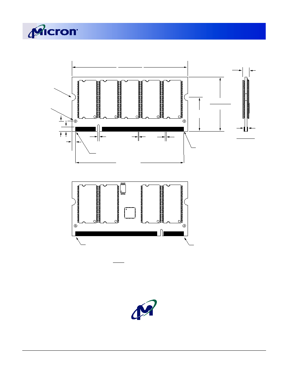
128MB, 256MB, 512MB, 1GB (x72, ECC, PLL)
200-PIN DDR SDRAM SODIMM
09005aef808ffdc7
Micron Technology, Inc., reserves the right to change products or specifications without notice.
DD9_18C16_32_64_128X72PHG_E.fm - Rev. E 7/03 EN
39
�2003 Micron Technology, Inc. All rights reserved.
�
8000 S. Federal Way, P.O. Box 6, Boise, ID 83707-0006, Tel: 208-368-3900
E-mail: prodmktg@micron.com, Internet: http://www.micron.com, Customer Comment Line: 800-932-4992
Micron, the M logo, and the Micron logo are trademarks and/or service marks of Micron Technology, Inc.
All other trademarks are the property of their respective owners.
Figure 16: Low-Profile 200-Pin SODIMM Dimensions
NOTE:
All dimensions are in inches (millimeters),
, or typical where noted.
Data Sheet Designation
Released: This data sheet contains minimum and
maximum limits specified over the complete power
supply and temperature range for production devices.
Although considered final, these specifications are sub-
ject to change, as further product development and
data characterization sometimes occur.
U1
U2
U3
U4
U5
U8
U7
U6
0.150 (3.80)
MAX
.043 (1.10)
.035 (0.90)
PIN 1
2.667 (67.75)
2.656 (67.45)
0.787 (20.00)
TYP
0.071 (1.80)
(2X)
0.024 (0.61)
TYP
0.018 (0.46)
TYP
0.079 (2.00) R
(2X)
PIN 199
PIN 200
PIN 2
FRONT VIEW
0.079 (2.00)
0.236 (6.00)
2.504 (63.60)
0.096 (2.44)
0.039 (0.99)
TYP
1.244 (31.60)
1.256 (31.90)
BACK VIEW
.320 (8.13)
MAX
Dual Rank Modules
0.043 (1.10)
0.035 (0.90)
U11
U10
U9
MAX
MIN