Document Outline
- Features/Options
- Ball Assignment, 66-Ball FBGA (Top View)
- General Description
- Table 1, VPP Voltage Ranges
- Device Marking
- Table 2, Cross Reference for Abbreviated Device Marks
- Part Numbering Information
- Figure 1, Part Number Chart
- Table 3, Valid Part Number Combinations
- Block Diagram
- Flash Functional Block Diagram
- Ball Descriptions
- Ball Descriptions (continued)
- Truth Table - Flash
- Truth Table - SRAM
- Architecture and Memory Organization
- Figure 2, Bottom Boot Block Device
- Figure 3, Top Boot Block Device
- Flash Memory Operating Modes
- Command State Machine
- Operations
- Command Definition
- Status Register
- Table 4, Command State Machine Codes For Device Mode Selection
- Command State Machine Operations
- Table 5, Command Definitions
- Table 6, Command Descriptions
- Table 6, Command Descriptions (continued)
- CLEAR STATUS REGISTER
- READ Operations
- Read Array
- Read Chip Identification Data
- Read Query
- Read Status Register
- Table 7, Command State Machine Transition Table
- Table 7, Command State Machine Transition Table (continued)
- Table 7, Command State Machine Transition Table (continued)
- Table 7, Command State Machine Transition Table (continued)
- Programming Operations
- ERASE Operation
- Table 8, Bus Operations
- Table 9, Status Register Bit Definition
- Figure 4, Automated Word Programming Flowchart
- Figure 5, PROGRAM SUSPEND/PROGRAM RESUME Flowchart
- Figure 6, BLOCK ERASE Flowchart
- Figure 7, ERASE SUSPEND/ERASE RESUME Flowchart
- READ-While-WRITE/ERASE Concurrency
- Figure 8, READ-While-WRITE Concurrency
- Figure 9a, Top Boot Block Device
- Figure 9b, Bottom Boot Block Device
- Block Locking
- Locked State
- Unlocked State
- Locked Down State
- Table 10, Block Locking State Transition
- Reading a Block's Lock Status
- Table 11, Chip Protection Configuration Addressing
- Locking Operations During ERASE SUSPEND
- Status Register Error Checking
- Chip Protection Register
- Reading the Chip Protection Register
- Figure 10, Protection Register Memory Map
- Page Read Mode
- Asynchronous READ Cycle
- Standby Mode
- Automatic Power Save Mode (APS)
- VPP/VCC Program and Erase Voltages
- Device Reset
- Power-Up Sequence
- Flash Electrical Specifications
- Absolute Maximum Ratings
- Recommended Operating Conditions
- Figure 11, Output Load Circuit
- Combined DC Characteristics
- Combined DC Characteristics (continued)
- Flash READ Cycle Timing Requirement, VCC = 1.65V-1.95V
- Flash READ Cycle Timing Requirement, VCC = 1.80V-2.20V
- Flash WRITE Cycle Timing Requirements
- Flash ERASE and PROGRAM Cycle Timing Requirements
- Flash Timing Diagrams
- Two-Cycle PROGRAMMING/ERASE Operation
- Asyncronous Page Mode READ Operation
- RESET Operation
- Table 15, CFI
- Table 15, CFI (continued)
- SRAM Operating Modes
- SRAM READ Array
- SRAM WRITE Array
- SRAM Functional Block Diagram
- Timing Test Conditions
- READ Cycle Timing
- WRITE Cycle Timing
- SRAM Timing Diagrams
- READ Cycle 1 (S_CE1# = S_OE# = VIL; S_CE2, S_WE# = VIH)
- READ Cycle 2 (S_WE# = VIH)
- WRITE Cycle (S_WE# Control)
- WRITE Cycle 2 (S_CE1# Control)
- 66-Ball FBGA
- Data Sheet Designation
1
2 Meg x 16 Page Flash 128K x 16 SRAM Combo Memory
©2002, Micron Technology, Inc.
MT28C3212P2FL_2.p65 ≠ Rev. 2, Pub. 4/02
2 MEG x 16 PAGE FLASH
128K x 16 SRAM COMBO MEMORY
PRODUCTS AND SPECIFICATIONS DISCUSSED HEREIN ARE SUBJECT TO CHANGE BY MICRON WITHOUT NOTICE.
FLASH AND SRAM
COMBO MEMORY
MT28C3212P2FL
MT28C3212P2NFL
Low Voltage, Extended Temperature
FEATURES
∑ Flexible dual-bank architecture
∑ Support for true concurrent operations with no
latency:
Read bank b during program bank a and vice versa
Read bank b during erase bank a and vice versa
∑ Organization: 2,048K x 16 (Flash)
128K x 16 (SRAM)
∑ Basic configuration:
Flash
Bank a (4Mb Flash for data storage)
≠ Eight 4K-word parameter blocks
≠ Seven 32K-word blocks
Bank b (28Mb Flash for program storage)
≠ Fifty-six 32K-word main blocks
SRAM
2Mb SRAM for data storage
≠ 128K-words
∑ F_V
CC
, V
CC
Q, F_V
PP
, S_V
CC
voltages
1
1.65V (MIN)/1.95V (MAX) F_V
CC
read voltage or
1.80V (MIN)/2.20V (MAX) F_V
CC
read voltage
1.65V (MIN)/1.95V (MAX) S_V
CC
read voltage or
1.80V (MIN)/2.20V (MAX) S_V
CC
read voltage
1.65V (MIN)/1.95V (MAX) V
CC
Q or
1.80V (MIN)/2.20V (MAX) V
CC
Q
1.80V (TYP) F_V
PP
(in-system PROGRAM/ERASE)
0.0V (MIN)/2.20V (MAX) F_V
PP
(in-system
PROGRAM/ERASE)
2
12V ±5% (HV) F_V
PP
(production programming
compatibility)
∑ Asynchronous access time
1
Flash access time: 100ns or 110ns @ 1.65V F_V
CC
SRAM access time: 100ns @ 1.65V S_V
CC
∑ Page Mode read access
1
Interpage read access: 100ns/110ns @ 1.65V F_V
CC
Intrapage read access: 35ns/45ns @ 1.65V F_V
CC
∑ Low power consumption
∑ Enhanced suspend options
ERASE-SUSPEND-to-READ within same bank
PROGRAM-SUSPEND-to-READ within same bank
ERASE-SUSPEND-to-PROGRAM within same bank
∑ Read/Write SRAM during program/erase of Flash
∑ Dual 64-bit chip protection registers for security
purposes
∑ PROGRAM/ERASE cycles
100,000 WRITE/ERASE cycles per block
∑ Cross-compatible command set support
Extended command set
Common Flash interface (CFI) compliant
NOTE: 1. These specifications are guaranteed for operation
within either one of two voltage ranges, 1.65V≠1.95V
or 1.80V≠2.20V. Use only one of the two voltage
ranges for PROGRAM and ERASE operations.
2. MT28C3212P2NFL only.
OPTIONS
MARKING
∑ Timing
100ns
-10
110ns
-11
∑ Boot Block
Top
T
Bottom
B
∑ V
PP
1
Range
0.9V≠2.2V
None
0.0V≠2.2V
N
∑ Operating Temperature Range
Commercial Temperature (0
o
C to +70
o
C) None
Extended Temperature (-40
o
C to +85
o
C)
ET
∑ Package
66-ball FBGA (8 x 8 grid)
FL
Part Number Example:
MT28C3212P2FL-10 TET
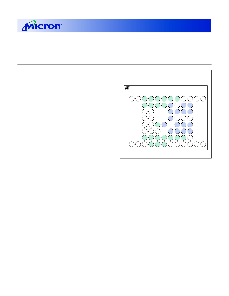
BALL ASSIGNMENT
66-Ball FBGA (Top View)
A
B
C
D
E
F
G
H
1 2 3 4 5 6 7 8 9 10
11
12
Top View
(Ball Down)
NC
NC
A14
A9
DQ11
A6
A0
A15
A10
A19
S_OE#
A7
A4
A20
A16
F_WE#
S_V
SS
F_WP#
S_LB#
A18
F_V
CC
A12
S_WE#
DQ6
S_CE2
DQ10
DQ8
A2
F_V
SS
F_V
SS
DQ14
DQ4
S_V
CC
DQ2
DQ0
A1
F_OE#
V
cc
Q
DQ7
DQ5
F_V
CC
DQ3
DQ1
S_CE1#
NC
NC
NC
NC
NC
A13
DQ15
DQ13
DQ12
DQ9
A3
F_CE#
NC
NC
A11
A8
NC
F_RP#
F_V
PP
S_UB#
A17
A5
2
2 Meg x 16 Page Flash 128K x 16 SRAM Combo Memory
Micron Technology, Inc., reserves the right to change products or specifications without notice.
MT28C3212P2FL_2.p65 ≠ Rev. 2, Pub. 4/02
©2002, Micron Technology, Inc.
2 MEG x 16 PAGE FLASH
128K x 16 SRAM COMBO MEMORY
Table 2
Cross Reference for Abbreviated Device Marks
PRODUCT
SAMPLE
MECHANICAL
PART NUMBER
MARKING
MARKING
SAMPLE MARKING
MT28C3212P2FL-10 BET
FW443
FX443
FY443
MT28C3212P2FL-10 TET
FW442
FX442
FY442
MT28C3212P2FL-11 BET
FW444
FX444
FY444
MT28C3212P2FL-11 TET
FW433
FX433
FY433
MT28C3212P2NFL-11 TET
FW445
FX445
FY445
GENERAL DESCRIPTION
The MT28C3212P2FL and MT28C3212P2NFL com-
bination Flash and SRAM memory devices provide a
compact, low-power solution for systems where PCB
real estate is at a premium. The dual-bank Flash is a
high-performance, high-density, nonvolatile memory
device with a revolutionary architecture that can sig-
nificantly improve system performance.
This new architecture features:
∑ A two-memory-bank configuration supporting
dual-bank burst operation;
∑ A high-performance bus interface providing a fast
page data transfer; and
∑ A conventional asynchronous bus interface.
The device also provides soft protection for blocks
by configuring soft protection registers with dedicated
command sequences. For security purposes, dual 64-
bit chip protection registers are provided.
The embedded WORD WRITE and BLOCK ERASE
functions are fully automated by an on-chip write state
machine (WSM). The WSM simplifies these operations
and relieves the system processor of secondary tasks.
An on-chip status register, one for each bank, can be
used to monitor the WSM status to determine the
progress of a PROGRAM/ERASE command.
The erase/program suspend functionality allows
compatibility with existing EEPROM emulation soft-
ware packages.
The device takes advantage of a dedicated power
source for the Flash device (F_V
CC
) and a dedicated
power source for the SRAM device (S_V
CC
), both at
1.65V≠1.95V or 1.80V≠2.20V for optimized power con-
sumption and improved noise immunity. The
MT28C3212P2FL and MT28C3212P2NFL devices sup-
port two V
PP
voltage ranges, V
PP
1
and V
PP
2
. V
PP
1
is an in-
circuit voltage of 0.9V≠2.2V (MT28C3212P2FL) or 0.0V≠
2.2V (MT28C3212P2NFL). V
PP
2
is the production com-
patibility voltage of 12V ±5%. The 12V ±5% V
PP
2
is sup-
ported for a maximum of 100 cycles and 10 cumulative
hours. See Table 1.
The MT28C3212P2FL and MT28C3212P2NFL de-
vices contain an asynchronous 2Mb SRAM organized
as 128K-words by 16 bits. These devices are fabricated
using an advanced CMOS process and high-speed/
ultra-low-power circuit technology.
The MT28C3212P2FL and MT28C3212P2NFL de-
vices are packaged in a 66-ball FBGA package with
0.80mm pitch.
DEVICE MARKING
Due to the size of the package, Micron's standard
part number is not printed on the top of each device.
Instead, an abbreviated device mark comprised of a
five-digit alphanumeric code is used. The abbreviated
device marks are cross referenced to Micron part num-
bers in Table 2.
Table 1
V
PP
Voltage Ranges
VOLTAGE RANGE
DEVICE
V
PP
1
V
PP
2
MT28C3212P2FL
0.9V≠2.2V
11.4V≠12.6V
MT28C3212P2NFL
0.0V≠2.2V
11.4V≠12.6V

3
2 Meg x 16 Page Flash 128K x 16 SRAM Combo Memory
Micron Technology, Inc., reserves the right to change products or specifications without notice.
MT28C3212P2FL_2.p65 ≠ Rev. 2, Pub. 4/02
©2002, Micron Technology, Inc.
2 MEG x 16 PAGE FLASH
128K x 16 SRAM COMBO MEMORY
PART NUMBERING INFORMATION
Micron's low-power devices are available with sev-
eral different combinations of features (see Figure 1).
Table 3
Valid Part Number Combinations
BOOT BLOCK
OPERATING
V
PP
1
ACCESS
STARTING
TEMPERATURE
PART NUMBER
RANGE
TIME (ns)
ADDRESS
RANGE
MT28C3212P2FL-10 BET
0.9V≠2.2V
100
Bottom
-40
o
C to +85
o
C
MT28C3212P2FL-10 TET
0.9V≠2.2V
100
Top
-40
o
C to +85
o
C
MT28C3212P2FL-11 BET
0.9V≠2.2V
110
Bottom
-40
o
C to +85
o
C
MT28C3212P2FL-11 TET
0.9V≠2.2V
110
Top
-40
o
C to +85
o
C
MT28C3212P2NFL-11 TET
0.0V≠2.2V
110
Top
-40
o
C to +85
o
C
MT 28C 321 2 P 2 N FL-11 T ET
Micron Technology
Flash Family
28C = Dual-Supply Flash/SRAM Combo
Density/Organization/Banks
321 = 32Mb (2,048K x 16)
bank a = 1/8; bank b = 7/8
SRAM Density
2 = 2Mb SRAM (128K x 16)
Access Time
-10 = 100ns
-11 = 110ns
Read Mode Operation
P = Asynchronous/Page Read
Package Code
FL = 66-ball FBGA (8 x 8 grid)
Operating Temperature Range
None = Commercial (0∫C to +70∫C)
ET = Extended (-40∫C to +85∫C)
V
PP1
Range
None = 0.9V≠2.2V
N = 0.0V≠2.2V
Boot Block Starting Address
B = Bottom boot
T = Top boot
Operating Voltage Range
2 = 1.65V≠1.95V or 1.80V≠2.20V
Figure 1
Part Number Chart
Valid combinations of features and their correspond-
ing part numbers are listed in Table 3.

4
2 Meg x 16 Page Flash 128K x 16 SRAM Combo Memory
Micron Technology, Inc., reserves the right to change products or specifications without notice.
MT28C3212P2FL_2.p65 ≠ Rev. 2, Pub. 4/02
©2002, Micron Technology, Inc.
2 MEG x 16 PAGE FLASH
128K x 16 SRAM COMBO MEMORY
BLOCK DIAGRAM
F_V
PP
S_OE#
S_CE2
S_CE1#
S_WE#
DQ0
≠
DQ15
A17
≠
A20
A0
≠
A16
F_RP#
F_CE#
F_OE#
F_WE#
F_V
CC
F_WP#
F_V
SS
FLASH
SRAM
S_V
SS
S_UB#
S_LB#
2,048K x 16
128K x 16
Bank a
Bank b
S_V
CC
V
CC
Q
FLASH FUNCTIONAL BLOCK DIAGRAM
Address
Input
Buffer
X DEC
Y/Z DEC
Data Input
Buffer
Output
Multiplexer
Address
CNT/WSM
Output
Buffer
Status
Reg.
WSM
Program/
Erase
Pump Voltage
Generators
Address Latch
DQ0-DQ15
DQ0≠DQ15
CSM
F_RST#
F_CE#
X DEC
Y/Z DEC
F_WE#
F_OE#
I/O Logic
A0≠A20
Address
Multiplexer
Bank 2 Blocks
Y/Z Gating/Sensing
Data
Register
Bank 1 Blocks
Y/Z Gating/Sensing
ID Reg.
RCR
Block Lock
Device ID
Manufacturer's ID
OTP
Query
PR Lock
Query/OTP
PR Lock

5
2 Meg x 16 Page Flash 128K x 16 SRAM Combo Memory
Micron Technology, Inc., reserves the right to change products or specifications without notice.
MT28C3212P2FL_2.p65 ≠ Rev. 2, Pub. 4/02
©2002, Micron Technology, Inc.
2 MEG x 16 PAGE FLASH
128K x 16 SRAM COMBO MEMORY
BALL DESCRIPTIONS
66-BALL FBGA
NUMBERS
SYMBOL
TYPE
DESCRIPTION
A3, A4, A5, A6,
A0≠A20
Input
Address Inputs: Inputs for the addresses during READ and WRITE
A7, A8, B3, B4,
operations. Addresses are internally latched during READ and WRITE
B5, B6, E5, G3,
cycles. Flash: A0≠A20; SRAM: A0≠A16.
G4, G5, G6, G7,
G8, G9, H4, H5,
H6
H7
F_CE#
Input
Flash Chip Enable: Activates the device when LOW. When CE# is HIGH,
the device is disabled and goes into standby power mode.
H9
F_OE#
Input
Flash Output Enable: Enables Flash output buffers when LOW. When
F_OE# is HIGH, the output buffers are disabled.
C3
F_WE#
Input
Flash Write Enable: Determines if a given cycle is a Flash WRITE cycle.
F_WE# is active LOW.
D4
F_RP#
Input
Reset. When F_RP# is a logic LOW, the device is in reset, which drives
the outputs to High-Z and resets the WSM. When F_RP# is a logic HIGH,
the device is in standard operation. When F_RP# transitions from logic
LOW to logic HIGH, the device resets all blocks to locked and defaults to
the read array mode.
E3
F_WP#
Input
Flash Write Protect. Controls the lock down function of the flexible
locking feature.
G10
S_CE1#
Input
SRAM Chip Enable1: Activates the SRAM when it is LOW. HIGH level
deselects the SRAM and reduces the power consumption to standby
levels.
D8
S_CE2
Input
SRAM Chip Enable2: Activates the SRAM when it is HIGH. LOW level
deselects the SRAM and reduces the power consumption to standby
levels.
F5
S_OE#
Input
SRAM Output Enable: Enables SRAM output buffers when LOW. When
S_OE# is HIGH, the output buffers are disabled.
B8
S_WE#
Input
SRAM Write Enable: Determines if a given cycle is an SRAM WRITE cycle.
S_WE# is active LOW.
F3
S_LB#
Input
SRAM Lower Byte: When LOW, it selects the SRAM address lower byte
(DQ0≠DQ7).
F4
S_UB#
Input
SRAM Upper Byte: When LOW, it selects the SRAM address upper byte
(DQ8≠DQ15).
B7, B9, B10,
DQ0≠DQ15
Input/
Data Inputs/Outputs: Input array data on the second CE# and WE#
C7, C8, C9,
Output
cycle during PROGRAM command. Input commands to the command
C10, D7, E6,
user interface when CE# and WE# are active. Output data when CE#
E8, E9, E10,
and OE# are active.
F7, F8, F9, F10
(continued on next page)