Document Outline
- Features
- Options
- General Description
- Functional Block Diagrams
- TQFP Pinouts
- TQFP Pin Assignment Table
- Pin Assignment (Top View)
- 100-Pin TQFP, 2-Chip Enable, T Version
- 100-Pin TQFP, 3-Chip Enable, S Version
- TQFP Pin Descriptions
- Pin Layout (Top View) 165-Pin FBGA
- FBGA Pin Descriptions
- Interleaved Burst Address Table (Mode = NC or HIGH)
- Linear Burst Address Table (Mode = LOW)
- Partial Truth Table for Write Commands (x18)
- Partial Truth Table for Write Commands (x32/x36)
- Truth Table
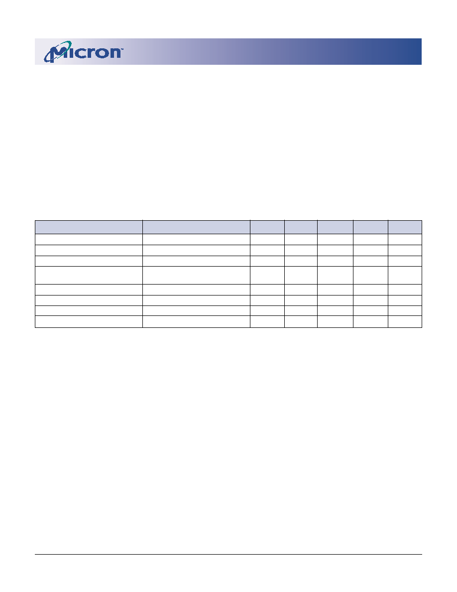
- Absolute Maximum Ratings
- 3.3V I/O DC Electrical Characteristics and Operating Conditions
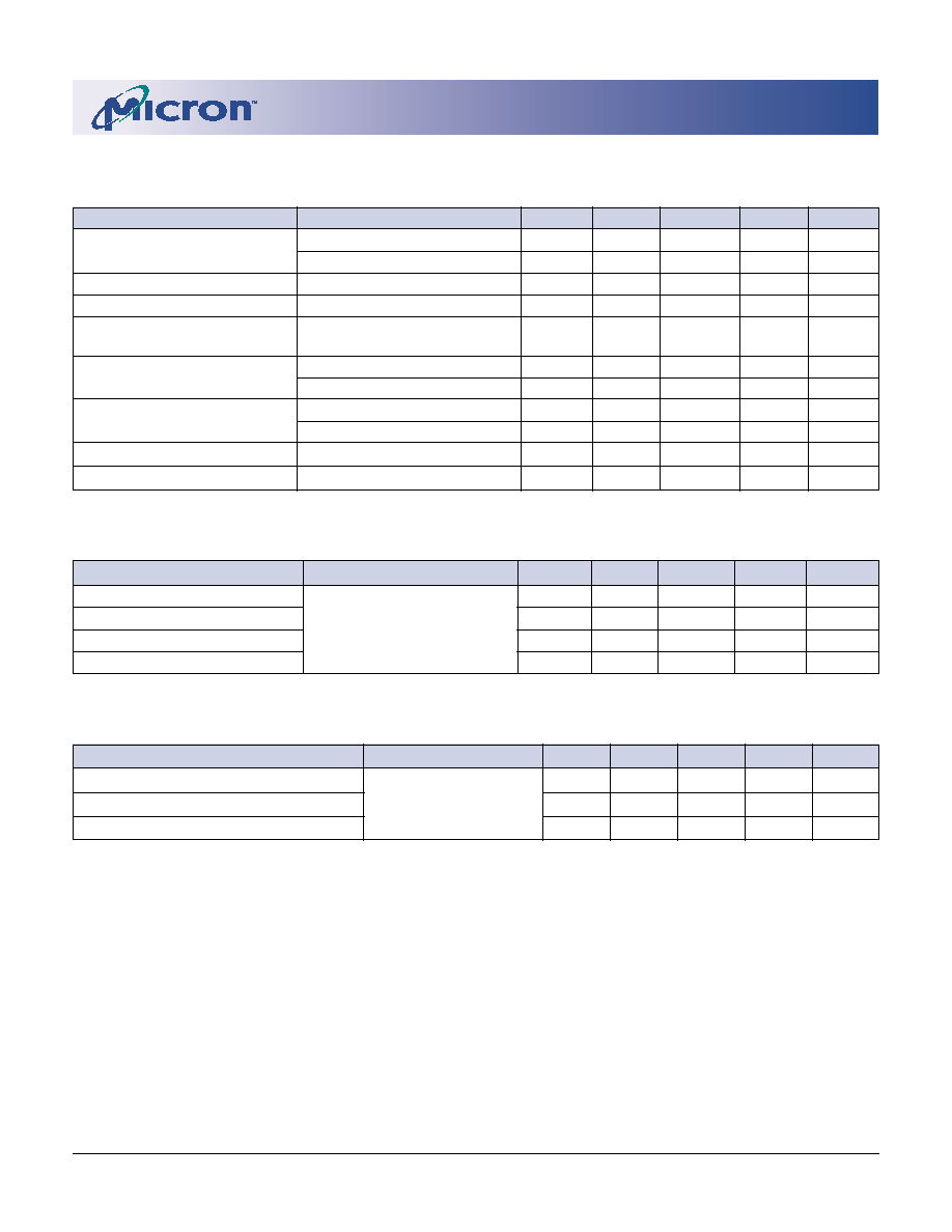
- 2.5V I/O DC Electrical Characteristics and Operating Conditions
- TQFP Capacitance
- FBGA Capacitance
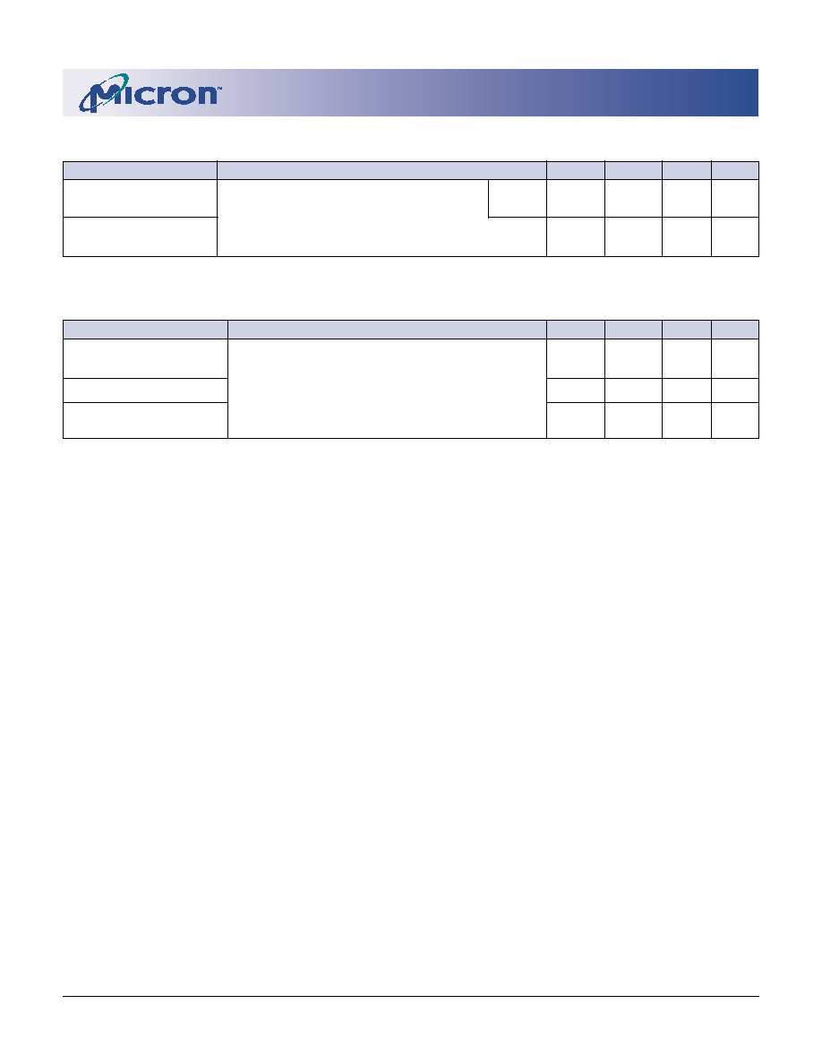
- TQFP Thermal Resistance
- FBGA Thermal Resistance
- IDD Operating Conditions and Maximum Limits
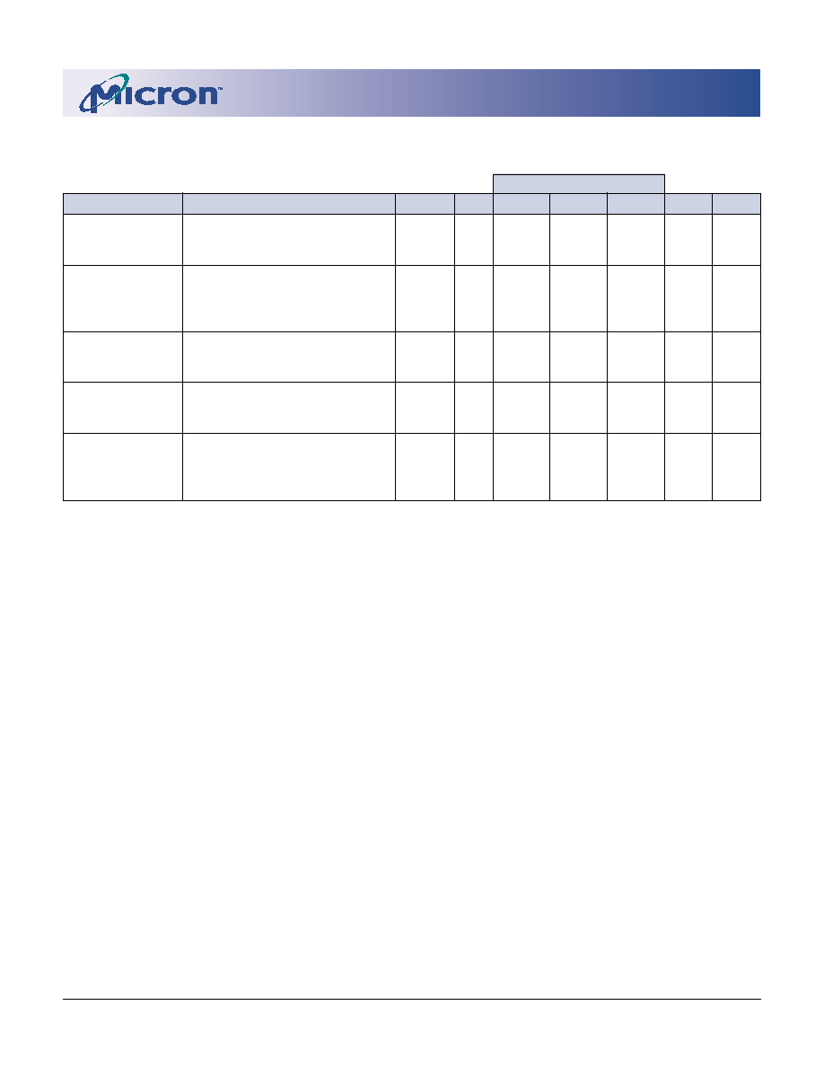
- Electrical Characteristics and Recommended AC Operating Conditions
- 3.3V I/O AC Test Conditions
- Figure 1 3.3V I/O Output Load Equivalent
- Figure 2 3.3V I/O Output Load Equivalent
- Load Derating Curves
- 2.5V I/O AC Test Conditions
- Figure 3 Output Load Equivalent
- Figure 4 2.5V I/O Output Load Equivalent
- Snooze Mode
- Snooze Mode Electrical Characteristics
- Snooze Mode Waveform
- Read Timing
- Write Timing
- Read/Write Timing
- 100-Pin Plastic TQFP (JEDEC LQFP)
- 165-Pin FBGA
- Revision History
1
8Mb: 512K x 18, 256K x 32/36 Pipelined, SCD SyncBurst SRAM
Micron Technology, Inc., reserves the right to change products or specifications without notice.
MT58L512L18P_C.p65 ≠ Rev. 2/02
©2002, Micron Technology, Inc.
8Mb: 512K x 18, 256K x 32/36
PIPELINED, SCD SYNCBURST SRAM
8Mb SYNCBURST
TM
SRAM
FEATURES
∑ Fast clock and OE# access times
∑ Single +3.3V +0.3V/-0.165V power supply (V
DD
)
∑ Separate +3.3V or +2.5V isolated output buffer
supply (V
DD
Q)
∑ SNOOZE MODE for reduced-power standby
∑ Single-cycle deselect (Pentium
Æ
BSRAM-compatible)
∑ Common data inputs and data outputs
∑ Individual BYTE WRITE control and GLOBAL
WRITE
∑ Three chip enables for simple depth expansion
and address pipelining
∑ Clock-controlled and registered addresses, data
I/Os and control signals
∑ Internally self-timed WRITE cycle
∑ Burst control (interleaved or linear burst)
∑ Automatic power-down for portable applications
∑ 100-pin TQFP package
∑ 165-pin FBGA package
∑ Low capacitive bus loading
∑ x18, x32, and x36 versions available
OPTIONS
MARKING
∑ Timing (Access/Cycle/MHz)
3.5ns/6ns/166 MHz
-6
4.0ns/7.5ns/133 MHz
-7.5
5ns/10ns/100 MHz
-10
∑ Configurations
3.3V I/O
512K x 18
MT58L512L18P
256K x 32
MT58L256L32P
256K x 36
MT58L256L36P
2.5V I/O
512K x 18
MT58L512V18P
256K x 32
MT58L256V32P
256K x 36
MT58L256V36P
∑ Packages
100-pin TQFP (2-chip enable)
T
100-pin TQFP (3-chip enable)
S
165-pin, 13mm x 15mm FBGA
F*
∑ Operating Temperature Range
Commercial (0∞C to +70∞C)
None
Industrial (-40∞C to +85∞C)**
IT
Part Number Example:
MT58L512L18PT-6
MT58L512L18P, MT58L256L32P, MT58L256L36P;
MT58L512V18P, MT58L256V32P, MT58L256V36P
3.3V V
DD
, 3.3V or 2.5V I/O, Pipelined, Single-Cycle
Deselect
NOTE: 1. JEDEC-standard MS-026 BHA (LQFP).
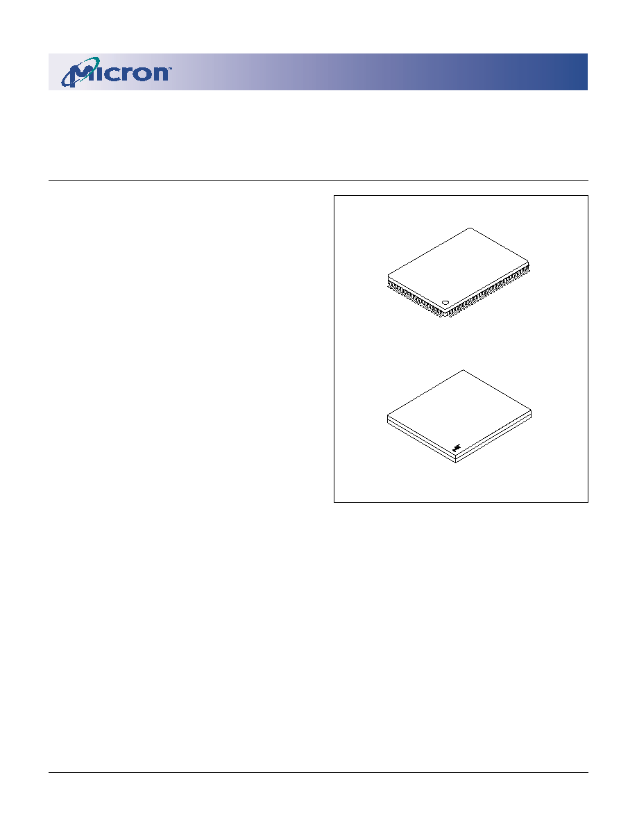
100-Pin TQFP
1
* A Part Marking Guide for the FBGA devices can be found on Micron's
Web site--
http://www.micron.com/support/index.html.
** Industrial temperature range offered in specific speed grades and
configurations. Contact factory for more information.
165-Pin FBGA
GENERAL DESCRIPTION
The Micron
Æ
SyncBurst
TM
SRAM family employs
high-speed, low-power CMOS designs that are fabri-
cated using an advanced CMOS process.
Micron's 8Mb SyncBurst SRAMs integrate a 512K x
18, 256K x 32, or 256K x 36 SRAM core with advanced
synchronous peripheral circuitry and a 2-bit burst
counter. All synchronous inputs pass through registers
controlled by a positive-edge-triggered single-clock in-
put (CLK). The synchronous inputs include all ad-
dresses, all data inputs, active LOW chip enable (CE#),
two additional chip enables for easy depth expansion
(CE2, CE2#), burst control inputs (ADSC#, ADSP#,
ADV#), byte write enables (BWx#) and global write
2
8Mb: 512K x 18, 256K x 32/36 Pipelined, SCD SyncBurst SRAM
Micron Technology, Inc., reserves the right to change products or specifications without notice.
MT58L512L18P_C.p65 ≠ Rev. 2/02
©2002, Micron Technology, Inc.
8Mb: 512K x 18, 256K x 32/36
PIPELINED, SCD SYNCBURST SRAM
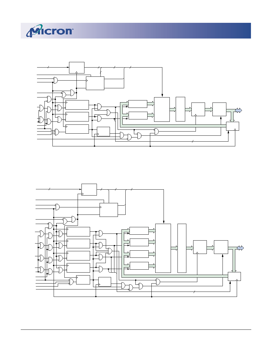
FUNCTIONAL BLOCK DIAGRAM
512K X 18
SA0, SA1, SAs
ADDRESS
REGISTER
ADV#
CLK
BINARY
COUNTER AND
LOGIC
CLR
Q1
Q0
ADSC#
19
19
17
19
BWb#
BWa#
CE#
BYTE "b"
WRITE REGISTER
BYTE "a"
WRITE REGISTER
ENABLE
REGISTER
SA0'
SA1'
OE#
SENSE
AMPS
512K x 9 x 2
MEMORY
ARRAY
ADSP#
2
SA0-SA1
MODE
CE2
CE2#
GW#
BWE#
PIPELINED
ENABLE
DQs
DQPa
DQPb
2
OUTPUT
REGISTERS
INPUT
REGISTERS
E
BYTE "b"
WRITE DRIVER
9
9
18
18
18
18
18
BYTE "a"
WRITE DRIVER
OUTPUT
BUFFERS
NOTE: Functional Block Diagrams illustrate simplified device operation. See Truth Table, Pin Descriptions, and timing diagrams
for detailed information.
FUNCTIONAL BLOCK DIAGRAM
256K X 32/36
ADDRESS
REGISTER
ADV#
CLK
BINARY
COUNTER
CLR
Q1
Q0
ADSP#
ADSC#
MODE
18
18
16
18
BWd#
BWc#
BWb#
BWa#
BWE#
GW#
CE#
CE2
CE2#
OE#
BYTE "d"
WRITE REGISTER
BYTE "c"
WRITE REGISTER
BYTE "b"
WRITE REGISTER
BYTE "a"
WRITE REGISTER
ENABLE
REGISTER
PIPELINED
ENABLE
DQs
DQPa
DQPb
DQPc
DQPd
4
OUTPUT
REGISTERS
SENSE
AMPS
256K x 8 x 4
(x32)
256K x 9 x 4
(x36)
MEMORY
ARRAY
OUTPUT
BUFFERS
E
BYTE "a"
WRITE DRIVER
BYTE "b"
WRITE DRIVER
BYTE "c"
WRITE DRIVER
9
9
36
36
36
36
36
9
9
INPUT
REGISTERS
SA0, SA1, SAs
SA0'
SA1'
SA0-SA1

3
8Mb: 512K x 18, 256K x 32/36 Pipelined, SCD SyncBurst SRAM
Micron Technology, Inc., reserves the right to change products or specifications without notice.
MT58L512L18P_C.p65 ≠ Rev. 2/02
©2002, Micron Technology, Inc.
8Mb: 512K x 18, 256K x 32/36
PIPELINED, SCD SYNCBURST SRAM
GENERAL DESCRIPTION (continued)
(GW#). Note that CE2# is not available on the
T Version.
Asynchronous inputs include the output enable
(OE#), clock (CLK) and snooze enable (ZZ). There is also
a burst mode input (MODE) that selects between inter-
leaved and linear burst modes. The data-out (Q), en-
abled by OE#, is also asynchronous. WRITE cycles can
be from one to two bytes wide (x18) or from one to four
bytes wide (x32/x36), as controlled by the write control
inputs.
Burst operation can be initiated with either address
status processor (ADSP#) or address status controller
(ADSC#) inputs. Subsequent burst addresses can be
internally generated as controlled by the burst advance
input (ADV#).
Address and write control are registered on-chip to
simplify WRITE cycles. This allows self-timed WRITE
cycles. Individual byte enables allow individual bytes
to be written. During WRITE cycles on the x18 device,
BWa# controls DQa pins and DQPa; BWb# controls
DQb pins and DQPb. During WRITE cycles on the x32
and x36 devices, BWa# controls DQa pins and DQPa;
BWb# controls DQb pins and DQPb; BWc# controls
DQc pins and DQPc; BWd# controls DQd pins and
DQPd. GW# LOW causes all bytes to be written. Parity
bits are only available on the x18 and x36 versions.
This device incorporates a single-cycle deselect fea-
ture during READ cycles. If the device is immediately
deselected after a READ cycle, the output bus goes to a
High-Z state
t
KQHZ nanoseconds after the rising edge
of clock.
Micron's 8Mb SyncBurst SRAMs operate from a
+3.3V V
DD
power supply, and all inputs and outputs are
TTL-compatible. Users can choose either a 3.3V or 2.5V
I/O version. The device is ideally suited for Pentium
and PowerPC pipelined systems and systems that ben-
efit from a very wide, high-speed data bus. The device
is also ideal in generic 16-, 18-, 32-, 36-, 64-, and 72-bit-
wide applications.
Please refer to Micron's Web site (
www.micron.com/
sramds
) for the latest data sheet.
TQFP PINOUTS
At the time of the writing of this data sheet, there are
two pinouts in the industry. Micron will support both
pinouts for this part.

4
8Mb: 512K x 18, 256K x 32/36 Pipelined, SCD SyncBurst SRAM
Micron Technology, Inc., reserves the right to change products or specifications without notice.
MT58L512L18P_C.p65 ≠ Rev. 2/02
©2002, Micron Technology, Inc.
8Mb: 512K x 18, 256K x 32/36
PIPELINED, SCD SYNCBURST SRAM
*No Function (NF) is used on the x32 version. Parity (DQPx) is used on the x36 version.
TQFP PIN ASSIGNMENT TABLE
PIN #
x18
x32/x36
1
NC
NF/
DQPc
*
2
NC
DQc
3
NC
DQc
4
V
DD
Q
5
V
SS
6
NC
DQc
7
NC
DQc
8
DQb
DQc
9
DQb
DQc
10
V
SS
11
V
DD
Q
12
DQb
DQc
13
DQb
DQc
14
V
DD
15
V
DD
16
NC
17
V
SS
18
DQb
DQd
19
DQb
DQd
20
V
DD
Q
21
V
SS
22
DQb
DQd
23
DQb
DQd
24
DQPb
DQd
25
NC
DQd
PIN #
x18
x32/x36
PIN #
x18
x32/x36
PIN #
x18
x32/x36
51
NC
NF/
DQPa
*
52
NC
DQa
53
NC
DQa
54
V
DD
Q
55
V
SS
56
NC
DQa
57
NC
DQa
58
DQa
59
DQa
60
V
SS
61
V
DD
Q
62
DQa
63
DQa
64
ZZ
65
V
DD
66
NC
67
V
SS
68
DQa
DQb
69
DQa
DQb
70
V
DD
Q
71
V
SS
72
DQa
DQb
73
DQa
DQb
74
DQPa
DQb
75
NC
DQb
26
V
SS
27
V
DD
Q
28
NC
DQd
29
NC
DQd
30
NC
NF/
DQPd
*
31
MODE
32
SA
33
SA
34
SA
35
SA
36
SA1
37
SA0
38
DNU
39
DNU
40
V
SS
41
V
DD
42
NF
43
NF (T Version)
SA
(S Version)
44
SA
45
SA
46
SA
47
SA
48
SA
49
SA
50
SA
76
V
SS
77
V
DD
Q
78
NC
DQb
79
NC
DQb
80
SA
NF/
DQPb
*
81
SA
82
SA
83
ADV#
84
ADSP#
85
ADSC#
86
OE#
87
BWE#
88
GW#
89
CLK
90
V
SS
91
V
DD
92
SA
(T Version)
CE2# (S Version)
93
BWa#
94
BWb#
95
NC
BWc#
96
NC
BWd#
97
CE2
98
CE#
99
SA
100
SA

5
8Mb: 512K x 18, 256K x 32/36 Pipelined, SCD SyncBurst SRAM
Micron Technology, Inc., reserves the right to change products or specifications without notice.
MT58L512L18P_C.p65 ≠ Rev. 2/02
©2002, Micron Technology, Inc.
8Mb: 512K x 18, 256K x 32/36
PIPELINED, SCD SYNCBURST SRAM
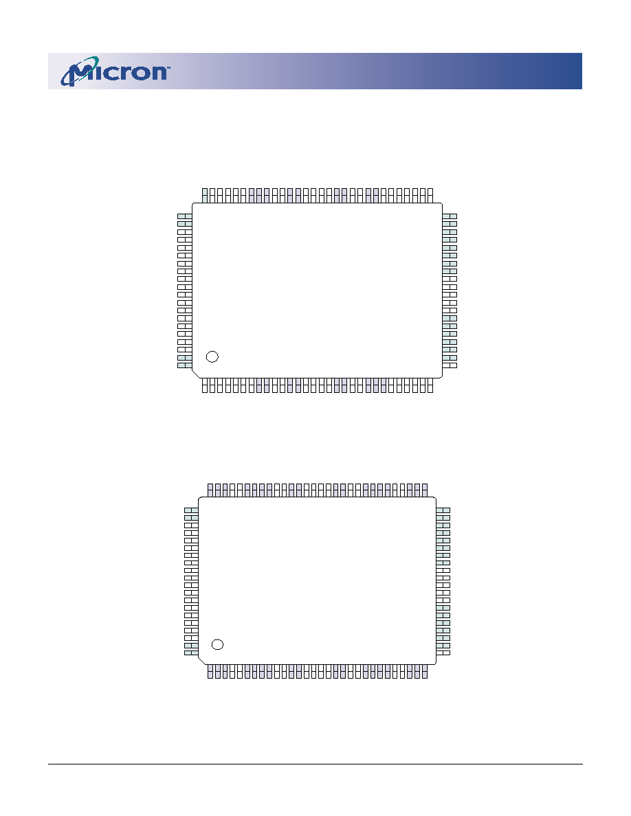
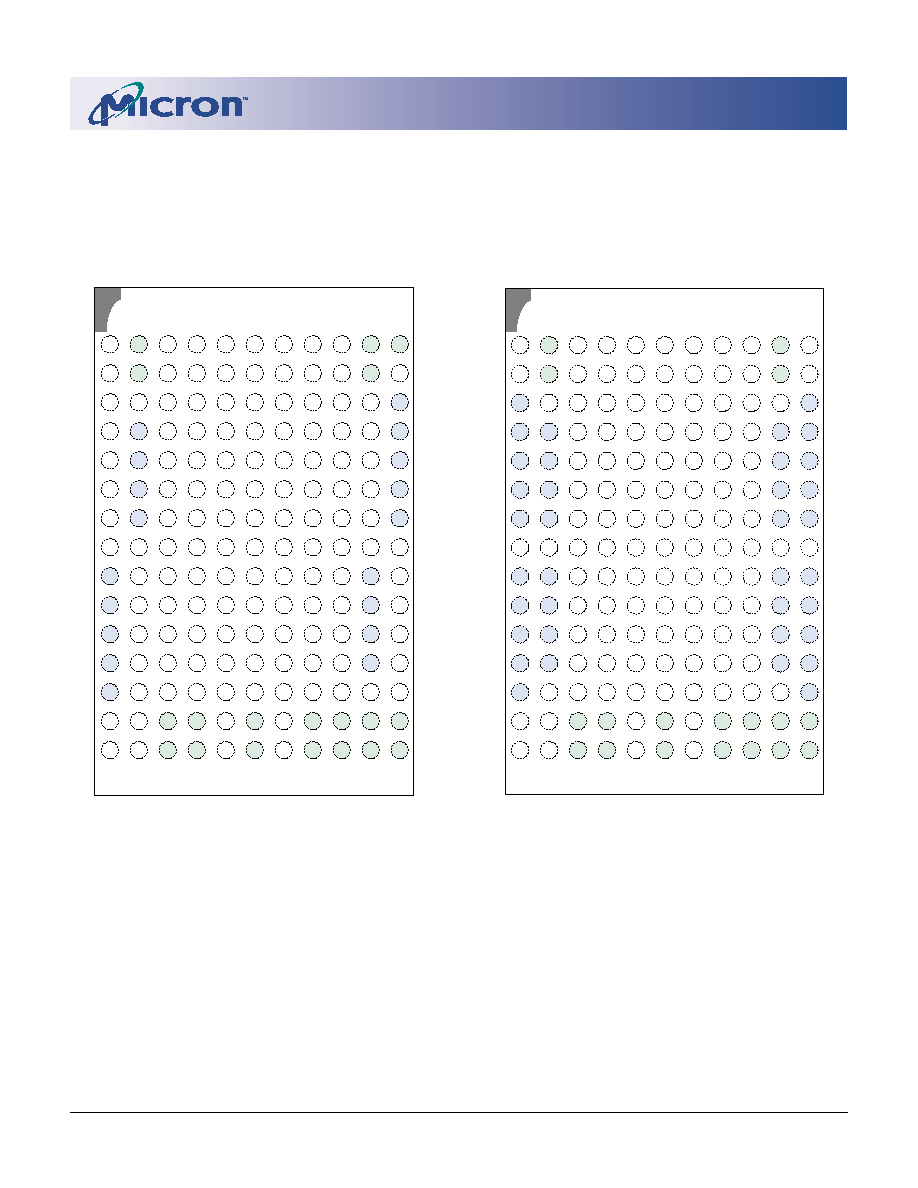
PIN ASSIGNMENT (TOP VIEW)
100-PIN TQFP, 2-CHIP ENABLE,
T VERSION
SA
SA
ADV#
ADSP#
ADSC#
OE#
BWE#
GW#
CLK
V
SS
V
DD
SA
BWa#
BWb#
NC
NC
CE2
CE#
SA
SA
81
82
83
84
85
86
87
88
89
90
91
92
93
94
95
96
97
98
99
100
50
49
48
47
46
45
44
43
42
41
40
39
38
37
36
35
34
33
32
31
80 79 78 77 76 75 74 73 72 71 70 69 68 67 66 65 64 63 62 61 60 59 58 57 56 55 54 53 52 51
1 2 3 4 5 6 7 8 9 10 11 12 13 14 15 16 17 18 19 20 21 22 23 24 25 26 27 28 29 30
SA
NC
NC
V
DD
Q
V
SS
NC
DQPa
DQa
DQa
V
SS
V
DD
Q
DQa
DQa
V
SS
NC
V
DD
ZZ
DQa
DQa
V
DD
Q
V
SS
DQa
DQa
NC
NC
V
SS
V
DD
Q
NC
NC
NC
SA
SA
SA
SA
SA
SA
SA
NF
NF
V
DD
V
SS
DNU
DNU
SA0
SA1
SA
SA
SA
SA
MODE
NC
NC
NC
V
DD
Q
V
SS
NC
NC
DQb
DQb
V
SS
V
DD
Q
DQb
DQb
V
DD
V
DD
NC
V
SS
DQb
DQb
V
DD
Q
V
SS
DQb
DQb
DQPb
NC
V
SS
V
DD
Q
NC
NC
NC
x18
SA
SA
ADV#
ADSP#
ADSC#
OE#
BWE#
GW#
CLK
V
SS
V
DD
SA
BWa#
BWb#
BWc#
BWd#
CE2
CE#
SA
SA
81
82
83
84
85
86
87
88
89
90
91
92
93
94
95
96
97
98
99
100
50
49
48
47
46
45
44
43
42
41
40
39
38
37
36
35
34
33
32
31
80 79 78 77 76 75 74 73 72 71 70 69 68 67 66 65 64 63 62 61 60 59 58 57 56 55 54 53 52 51
1 2 3 4 5 6 7 8 9 10 11 12 13 14 15 16 17 18 19 20 21 22 23 24 25 26 27 28 29 30
NF/
DQPb
*
DQb
DQb
V
DD
Q
V
SS
DQb
DQb
DQb
DQb
V
SS
V
DD
Q
DQb
DQb
V
SS
NC
V
DD
ZZ
DQa
DQa
V
DD
Q
V
SS
DQa
DQa
DQa
DQa
V
SS
V
DD
Q
DQa
DQa
NF/
DQPa
*
SA
SA
SA
SA
SA
SA
SA
NF
NF
V
DD
V
SS
DNU
DNU
SA0
SA1
SA
SA
SA
SA
MODE
NF/
DQPc
*
DQc
DQc
V
DD
Q
V
SS
DQc
DQc
DQc
DQc
V
SS
V
DD
Q
DQc
DQc
V
DD
V
DD
NC
V
SS
DQd
DQd
V
DD
Q
V
SS
DQd
DQd
DQd
DQd
V
SS
V
DD
Q
DQd
DQd
NF/
DQPd
*
x32/x36
*No Function (NF) is used on the x32 version. Parity (DQPx) is used on the x36 version.
6
8Mb: 512K x 18, 256K x 32/36 Pipelined, SCD SyncBurst SRAM
Micron Technology, Inc., reserves the right to change products or specifications without notice.
MT58L512L18P_C.p65 ≠ Rev. 2/02
©2002, Micron Technology, Inc.
8Mb: 512K x 18, 256K x 32/36
PIPELINED, SCD SYNCBURST SRAM
PIN ASSIGNMENT (TOP VIEW)
100-PIN TQFP, 3-CHIP ENABLE,
S VERSION
SA
SA
ADV#
ADSP#
ADSC#
OE#
BWE#
GW#
CLK
V
SS
V
DD
CE2#
BWa#
BWb#
NC
NC
CE2
CE#
SA
SA
81
82
83
84
85
86
87
88
89
90
91
92
93
94
95
96
97
98
99
100
50
49
48
47
46
45
44
43
42
41
40
39
38
37
36
35
34
33
32
31
80 79 78 77 76 75 74 73 72 71 70 69 68 67 66 65 64 63 62 61 60 59 58 57 56 55 54 53 52 51
1 2 3 4 5 6 7 8 9 10 11 12 13 14 15 16 17 18 19 20 21 22 23 24 25 26 27 28 29 30
SA
NC
NC
V
DD
Q
V
SS
NC
DQPa
DQa
DQa
V
SS
V
DD
Q
DQa
DQa
V
SS
NC
V
DD
ZZ
DQa
DQa
V
DD
Q
V
SS
DQa
DQa
NC
NC
V
SS
V
DD
Q
NC
NC
NC
SA
SA
SA
SA
SA
SA
SA
SA
NF
V
DD
V
SS
DNU
DNU
SA0
SA1
SA
SA
SA
SA
MODE
NC
NC
NC
V
DD
Q
V
SS
NC
NC
DQb
DQb
V
SS
V
DD
Q
DQb
DQb
V
DD
V
DD
NC
V
SS
DQb
DQb
V
DD
Q
V
SS
DQb
DQb
DQPb
NC
V
SS
V
DD
Q
NC
NC
NC
x18
SA
SA
ADV#
ADSP#
ADSC#
OE#
BWE#
GW#
CLK
V
SS
V
DD
CE2#
BWa#
BWb#
BWc#
BWd#
CE2
CE#
SA
SA
81
82
83
84
85
86
87
88
89
90
91
92
93
94
95
96
97
98
99
100
50
49
48
47
46
45
44
43
42
41
40
39
38
37
36
35
34
33
32
31
80 79 78 77 76 75 74 73 72 71 70 69 68 67 66 65 64 63 62 61 60 59 58 57 56 55 54 53 52 51
1 2 3 4 5 6 7 8 9 10 11 12 13 14 15 16 17 18 19 20 21 22 23 24 25 26 27 28 29 30
NF/
DQPb
*
DQb
DQb
V
DD
Q
V
SS
DQb
DQb
DQb
DQb
V
SS
V
DD
Q
DQb
DQb
V
SS
NC
V
DD
ZZ
DQa
DQa
V
DD
Q
V
SS
DQa
DQa
DQa
DQa
V
SS
V
DD
Q
DQa
DQa
NF/
DQPa
*
SA
SA
SA
SA
SA
SA
SA
SA
NF
V
DD
V
SS
DNU
DNU
SA0
SA1
SA
SA
SA
SA
MODE
NF/
DQPc
*
DQc
DQc
V
DD
Q
V
SS
DQc
DQc
DQc
DQc
V
SS
V
DD
Q
DQc
DQc
V
DD
V
DD
NC
V
SS
DQd
DQd
V
DD
Q
V
SS
DQd
DQd
DQd
DQd
V
SS
V
DD
Q
DQd
DQd
NF/
DQPd
*
x32/x36
*No Function (NF) is used on the x32 version. Parity (DQPx) is used on the x36 version.
7
8Mb: 512K x 18, 256K x 32/36 Pipelined, SCD SyncBurst SRAM
Micron Technology, Inc., reserves the right to change products or specifications without notice.
MT58L512L18P_C.p65 ≠ Rev. 2/02
©2002, Micron Technology, Inc.
8Mb: 512K x 18, 256K x 32/36
PIPELINED, SCD SYNCBURST SRAM
TQFP PIN DESCRIPTIONS
x18
x32/x36
SYMBOL
TYPE
DESCRIPTION
37
37
SA0
Input
Synchronous Address Inputs: These inputs are registered and must
36
36
SA1
meet the setup and hold times around the rising edge of CLK. Two
32-35, 44-50,
32-35, 44-50,
SA
different pinouts are available for the TQFP package.
80-82, 99,
81, 82, 99,
100
100
92
(T Version)
92
(T Version)
43
(S Version)
43
(S Version)
93
93
BWa#
Input
Synchronous Byte Write Enables: These active LOW inputs allow
94
94
BWb#
individual bytes to be written and must meet the setup and hold
≠
95
BWc#
times around the rising edge of CLK. A byte write enable is LOW
≠
96
BWd#
for a WRITE cycle and HIGH for a READ cycle. For the x18 version,
BWa# controls DQa pins and DQPa; BWb# controls DQb pins and
DQPb. For the x32 and x36 versions, BWa# controls DQa pins and
DQPa; BWb# controls DQb pins and DQPb; BWc# controls DQc pins
and DQPc; BWd# controls DQd pins and DQPd. Parity is only available
on the x18 and x36 versions.
87
87
BWE#
Input
Byte Write Enable: This active LOW input permits BYTE WRITE
operations and must meet the setup and hold times around the
rising edge of CLK.
88
88
GW#
Input
Global Write: This active LOW input allows a full 18-, 32- or 36-bit
WRITE to occur independent of the BWE# and BWx# lines and must
meet the setup and hold times around the rising edge of CLK.
89
89
CLK
Input
Clock: This signal registers the address, data, chip enable, byte write
enables and burst control inputs on its rising edge. All synchronous
inputs must meet setup and hold times around the clock's rising
edge.
98
98
CE#
Input
Synchronous Chip Enable: This active LOW input is used to enable
the device and conditions the internal use of ADSP#. CE# is sampled
only when a new external address is loaded.
92
92
CE2#
Input
Synchronous Chip Enable: This active LOW input is used to enable
(S Version)
(S Version)
the device and is sampled only when a new external address is
loaded. CE2# is only available on the S version.
64
64
ZZ
Input
Snooze Enable: This active HIGH, asynchronous input causes the
device to enter a low-power standby mode in which all data in the
memory array is retained. When ZZ is active, all other inputs are
ignored.
97
97
CE2
Input
Synchronous Chip Enable: This active HIGH input is used to enable
the device and is sampled only when a new external address is
loaded.
86
86
OE#
Input
Output Enable: This
active LOW, asynchronous input enables the
data I/O output drivers.
83
83
ADV#
Input
Synchronous Address Advance: This active LOW input is used to
advance the internal burst counter, controlling burst access after the
external address is loaded. A HIGH on this pin effectively causes wait
states to be generated (no address advance). To ensure use of correct
address during a WRITE cycle, ADV# must be HIGH at the rising edge
of the first clock after an ADSP# cycle is initiated.
(continued on next page)

8
8Mb: 512K x 18, 256K x 32/36 Pipelined, SCD SyncBurst SRAM
Micron Technology, Inc., reserves the right to change products or specifications without notice.
MT58L512L18P_C.p65 ≠ Rev. 2/02
©2002, Micron Technology, Inc.
8Mb: 512K x 18, 256K x 32/36
PIPELINED, SCD SYNCBURST SRAM
TQFP PIN DESCRIPTIONS (continued)
x18
x32/x36
SYMBOL
TYPE
DESCRIPTION
84
84
ADSP#
Input
Synchronous Address Status Processor: This active LOW input
interrupts any ongoing burst, causing a new external address to be
registered. A READ is performed using the new address, independent
of the byte write enables and ADSC#, but dependent upon CE#, CE2
and CE2#. ADSP# is ignored if CE# is HIGH. Power-down state is
entered if CE2 is LOW or CE2# is HIGH.
85
85
ADSC#
Input
Synchronous Address Status Controller: This active LOW input
interrupts any ongoing burst, causing a new external address to be
registered. A READ or WRITE is performed using the new address if
CE# is LOW. ADSC# is also used to place the chip into power-down
state when CE# is HIGH.
31
31
MODE
Input
Mode: This input selects the burst sequence. A LOW on this pin
selects "linear burst." NC or HIGH on this pin selects "interleaved
burst." Do not alter input state while device is operating.
(a) 58, 59,
(a) 52, 53,
DQa
Input/ SRAM Data I/Os: For the x18 version, Byte "a" is DQa pins; Byte "b"
62, 63, 68, 69, 56-59, 62, 63
Output is DQb pins. For the x32 and x36 versions, Byte "a" is DQa pins;
72, 73
Byte "b" is DQb pins; Byte "c" is DQc pins; Byte "d" is DQd pins.
(b) 8, 9, 12,
(b) 68, 69
DQb
Input data must meet setup and hold times around the rising edge
13, 18, 19, 22, 72-75, 78, 79
of CLK.
23
(c) 2, 3, 6-9,
DQc
12, 13
(d) 18, 19,
DQd
22-25, 28, 29
74
51
NF/
DQPa
NF /
No Function/Parity Data I/Os: On the x32 version, these pins are No
24
80
NF/
DQPb
I/O
Function (NF). On the x18 version, Byte "a" parity is DQPa; Byte "b"
≠
1
NF/
DQPc
parity is DQPb. On the x36 version, Byte "a" parity is DQPa; Byte "b"
≠
30
NF/
DQPd
parity is DQPb; Byte "c" parity is DQPc; Byte "d" parity is DQPd.
14, 15, 41, 65, 14, 15, 41, 65,
V
DD
Supply Power Supply:
See DC Electrical Characteristics and Operating
91
91
Conditions for range.
4, 11, 20, 27,
4, 11, 20, 27,
V
DD
Q
Supply Isolated Output Buffer Supply: See DC Electrical Characteristics and
54, 61, 70, 77 54, 61, 70, 77
Operating Conditions for range.
5, 10, 17, 21,
5, 10, 17, 21,
V
SS
Supply Ground:
GND.
26, 40, 55, 60, 26, 40, 55, 60,
67, 71, 76, 90 67, 71, 76, 90
38, 39
38, 39
DNU
≠
Do Not Use: These signals may either be unconnected or wired to
GND to improve package heat dissipation.
1-3, 6, 7,
16, 66
NC
≠
No Connect: These signals are not internally connected and may be
16, 25, 28-30,
connected to ground to improve package heat dissipation.
51-53, 56, 57,
66, 75, 78, 79,
95, 96
42
42
NF
≠
No Function: These pins are internally connected to the die and
43 (T Version) 43 (T Version)
have the capacitance of an input pin. It is allowable to leave these
pins unconnected or driven by signals. On the S version, pin 42 is
reserved as an address upgrade pin for the 18Mb SyncBurst SRAM.
9
8Mb: 512K x 18, 256K x 32/36 Pipelined, SCD SyncBurst SRAM
Micron Technology, Inc., reserves the right to change products or specifications without notice.
MT58L512L18P_C.p65 ≠ Rev. 2/02
©2002, Micron Technology, Inc.
8Mb: 512K x 18, 256K x 32/36
PIPELINED, SCD SYNCBURST SRAM
PIN LAYOUT (TOP VIEW)
165-PIN FBGA
A
B
C
D
E
F
G
H
J
K
L
M
N
P
R
A
B
C
D
E
F
G
H
J
K
L
M
N
P
R
2
CE#
CE2
V
DD
Q
V
DD
Q
V
DD
Q
V
DD
Q
V
DD
Q
NC
V
DD
Q
V
DD
Q
V
DD
Q
V
DD
Q
V
DD
Q
SA
SA
SA
SA
NC
DQb
DQb
DQb
DQb
V
SS
NC
NC
NC
NC
NC
NC
NC
NC
NC
NC
NC
NC
NC
NC
V
DD
DQb
DQb
DQb
DQb
NF/
DQPb
NC
MODE
(LBO#)
BWb#
NC
V
SS
V
DD
V
DD
V
DD
V
DD
V
DD
V
DD
V
DD
V
DD
V
DD
V
SS
SA
SA
NC
BWa#
V
SS
V
SS
V
SS
V
SS
V
SS
V
SS
V
SS
V
SS
V
SS
V
SS
NC
DNU
DNU
CE2#
CLK
V
SS
V
SS
V
SS
V
SS
V
SS
V
SS
V
SS
V
SS
V
SS
V
SS
NC
SA1
SA0
BWE#
GW#
V
SS
V
SS
V
SS
V
SS
V
SS
V
SS
V
SS
V
SS
V
SS
V
SS
V
SS
DNU
DNU
ADSC#
OE# (G#)
V
SS
V
DD
V
DD
V
DD
V
DD
V
DD
V
DD
V
DD
V
DD
V
DD
V
SS
SA
SA
ADV#
ADSP#
V
DD
Q
V
DD
Q
V
DD
Q
V
DD
Q
V
DD
Q
NC
V
DD
Q
V
DD
Q
V
DD
Q
V
DD
Q
V
DD
Q
SA
SA
SA
SA
NC
NC
NC
NC
NC
NC
DQa
DQa
DQa
DQa
NC
SA
SA
SA
NC
NF/
DQPa
DQa
DQa
DQa
DQa
ZZ
NC
NC
NC
NC
NC
SA
SA
TOP VIEW
3
4
5
6
7
8
9
10
11
1
A
B
C
D
E
F
G
H
J
K
L
M
N
P
R
A
B
C
D
E
F
G
H
J
K
L
M
N
P
R
2
CE#
CE2
V
DD
Q
V
DD
Q
V
DD
Q
V
DD
Q
V
DD
Q
NC
V
DD
Q
V
DD
Q
V
DD
Q
V
DD
Q
V
DD
Q
SA
SA
SA
SA
NC
DQc
DQc
DQc
DQc
V
SS
DQd
DQd
DQd
DQd
NC
NC
NC
NC
NC
NF/
DQPc
DQc
DQc
DQc
DQc
V
DD
DQd
DQd
DQd
DQd
NF/
DQPd
NC
MODE
(LBO#)
BWc#
BWd#
V
SS
V
DD
V
DD
V
DD
V
DD
V
DD
V
DD
V
DD
V
DD
V
DD
V
SS
SA
SA
BWb#
BWa#
V
SS
V
SS
V
SS
V
SS
V
SS
V
SS
V
SS
V
SS
V
SS
V
SS
NC
DNU
DNU
CE2#
CLK
V
SS
V
SS
V
SS
V
SS
V
SS
V
SS
V
SS
V
SS
V
SS
V
SS
NC
SA1
SA0
BWE#
GW#
V
SS
V
SS
V
SS
V
SS
V
SS
V
SS
V
SS
V
SS
V
SS
V
SS
V
SS
DNU
DNU
ADSC#
OE# (G#)
V
SS
V
DD
V
DD
V
DD
V
DD
V
DD
V
DD
V
DD
V
DD
V
DD
V
SS
SA
SA
ADV#
ADSP#
V
DD
Q
V
DD
Q
V
DD
Q
V
DD
Q
V
DD
Q
NC
V
DD
Q
V
DD
Q
V
DD
Q
V
DD
Q
V
DD
Q
SA
SA
SA
SA
NC
DQb
DQb
DQb
DQb
NC
DQa
DQa
DQa
DQa
NC
SA
SA
NC
NC
NF/
DQPb
DQb
DQb
DQb
DQb
ZZ
DQa
DQa
DQa
DQa
NF/
DQPa
SA
SA
TOP VIEW
3
4
5
6
7
8
9
10
11
1
x18
x32/x36
*No Function (NF) is used on the x32 version. Parity (DQPx) is used on the x36 version.
10
8Mb: 512K x 18, 256K x 32/36 Pipelined, SCD SyncBurst SRAM
Micron Technology, Inc., reserves the right to change products or specifications without notice.
MT58L512L18P_C.p65 ≠ Rev. 2/02
©2002, Micron Technology, Inc.
8Mb: 512K x 18, 256K x 32/36
PIPELINED, SCD SYNCBURST SRAM
FBGA PIN DESCRIPTIONS
x18
x32/x36
SYMBOL
TYPE
DESCRIPTION
6R
6R
SA0
Input
Synchronous Address Inputs: These inputs are registered and must
6P
6P
SA1
meet the setup and hold times around the rising edge of CLK.
2A, 2B, 3P,
2A, 2B, 3P,
SA
3R, 4P, 4R,
3R, 4P, 4R,
8P, 8R, 9P, 9R,
8P, 8R, 9P,
10A, 10B, 10P, 9R, 10A, 10B,
10R, 11A, 11P, 10P, 10R, 11P,
11R
11R
5B
5B
BWa#
Input
Synchronous Byte Write Enables: These active LOW inputs allow
4A
5A
BWb#
individual bytes to be written and must meet the setup and hold
≠
4A
BWc#
times around the rising edge of CLK. A byte write enable is LOW
≠
4B
BWd#
for a WRITE cycle and HIGH for a READ cycle. For the x18 version,
BWa# controls DQa's and DQPa; BWb# controls DQb's and DQPb.
For the x32 and x36 versions, BWa# controls DQa's and DQPa; BWb#
controls DQb's and DQPb; BWc# controls DQc's and DQPc; BWd#
controls DQd's and DQPd. Parity is only available on the x18 and x36
versions.
7A
7A
BWE#
Input
Byte Write Enable: This active LOW input permits BYTE WRITE
operations and must meet the setup and hold times around the
rising edge of CLK.
7B
7B
GW#
Input
Global Write: This active LOW input allows a full 18-, 32- or 36-bit
WRITE to occur independent of the BWE# and BWx# lines and must
meet the setup and hold times around the rising edge of CLK.
6B
6B
CLK
Input
Clock: This signal registers the address, data, chip enable, byte write
enables, and burst control inputs on its rising edge. All synchronous
inputs must meet setup and hold times around the clock's rising
edge.
3A
3A
CE#
Input
Synchronous Chip Enable: This active LOW input is used to enable
the device and conditions the internal use of ADSP#. CE# is sampled
only when a new external address is loaded.
6A
6A
CE2#
Input
Synchronous Chip Enable: This active LOW input is used to enable
the device and is sampled only when a new external address is
loaded.
11H
11H
ZZ
Input
Snooze Enable: This active HIGH, asynchronous input causes the
device to enter a low-power standby mode in which all data in the
memory array is retained. When ZZ is active, all other inputs are
ignored.
3B
3B
CE2
Input
Synchronous Chip Enable: This active HIGH input is used to enable
the device and is sampled only when a new external address is
loaded.
8B
8B
OE#(G#)
Input
Output Enable: This
active LOW, asynchronous input enables the
data I/O output drivers.
(continued on next page)

11
8Mb: 512K x 18, 256K x 32/36 Pipelined, SCD SyncBurst SRAM
Micron Technology, Inc., reserves the right to change products or specifications without notice.
MT58L512L18P_C.p65 ≠ Rev. 2/02
©2002, Micron Technology, Inc.
8Mb: 512K x 18, 256K x 32/36
PIPELINED, SCD SYNCBURST SRAM
FBGA PIN DESCRIPTIONS (continued)
x18
x32/x36
SYMBOL
TYPE
DESCRIPTION
9A
9A
ADV#
Input
Synchronous Address Advance: This active LOW input is used to
advance the internal burst counter, controlling burst access after
the external address is loaded. A HIGH on ADV# effectively causes
wait states to be generated (no address advance). To ensure use of
correct address during a WRITE cycle, ADV# must be HIGH at the
rising edge of the first clock after an ADSP# cycle is initiated.
9B
9B
ADSP#
Input
Synchronous Address Status Processor: This active LOW input
interrupts any ongoing burst, causing a new external address to be
registered. A READ is performed using the new address,
independent of the byte write enables and ADSC#, but dependent
upon CE#, CE2 and CE2#. ADSP# is ignored if CE# is HIGH. Power-
down state is entered if CE2 is LOW or CE2# is HIGH.
8A
8A
ADSC#
Input
Synchronous Address Status Controller: This active LOW input
interrupts any ongoing burst, causing a new external address to be
registered. A READ or WRITE is performed using the new address if
CE# is LOW. ADSC# is also used to place the chip into power-down
state when CE# is HIGH.
1R
1R
MODE
Input
Mode: This input selects the burst sequence. A LOW on this input
(LB0#)
selects "linear burst." NC or HIGH on this input selects "interleaved
burst." Do not alter input state while device is operating.
(a)
10J, 10K,
(a)
10J, 10K,
DQa
Input/ SRAM Data I/Os: For the x18 version, Byte "a" is associated DQa's;
10L, 10M, 11D, 10L, 10M, 11J,
Output Byte "b" is associated with DQb's. For the x32 and x36 versions,
11E, 11F, 11G 11K, 11L, 11M
Byte "a" is associated with DQa's; Byte "b" is associated with DQb's;
(b)
1J, 1K,
(b)
10D, 10E,
DQb
Byte "c" is associated with DQc's; Byte "d" is associated with DQd's.
1L, 1M, 2D,
10F, 10G, 11D,
Input data must meet setup and hold times around the rising edge
2E, 2F, 2G
11E, 11F, 11G
of CLK.
(c)
1D, 1E,
DQc
1F, 1G, 2D,
2E, 2F, 2G
(d)
1J, 1K, 1L,
DQd
1M, 2J, 2K,
2L, 2M
11C
11N
NF/
DQPa
NF/
No Function/Parity Data I/Os: On the x32 version, these are No
1N
11C
NF/
DQPb
I/O
Function (NF). On the x18 version, Byte "a" parity is DQPa; Byte "b"
≠
1C
NF/
DQPc
parity is DQPb. On the x36 version, Byte "a" parity is DQPa; Byte
≠
1N
NF/
DQPd
"b" parity is DQPb; Byte "c" parity is DQPc; Byte "d" parity is DQPd.
1H, 4D, 4E, 4F, 1H, 4D, 4E, 4F,
V
DD
Supply Power Supply:
See DC Electrical Characteristics and Operating
4G, 4H, 4J,
4G, 4H, 4J,
Conditions for range.
4K, 4L, 4M,
4K, 4L, 4M,
8D, 8E, 8F,
8D, 8E, 8F,
8G, 8H, 8J,
8G, 8H, 8J,
8K, 8L, 8M
8K, 8L, 8M
(continued on next page)
12
8Mb: 512K x 18, 256K x 32/36 Pipelined, SCD SyncBurst SRAM
Micron Technology, Inc., reserves the right to change products or specifications without notice.
MT58L512L18P_C.p65 ≠ Rev. 2/02
©2002, Micron Technology, Inc.
8Mb: 512K x 18, 256K x 32/36
PIPELINED, SCD SYNCBURST SRAM
FBGA PIN DESCRIPTIONS (continued)
x18
x32/x36
SYMBOL
TYPE
DESCRIPTION
3C, 3D, 3E,
3C, 3D, 3E,
V
DD
Q
Supply Isolated Output Buffer Supply: See DC Electrical Characteristics and
3F, 3G, 3J,
3F, 3G, 3J,
Operating Conditions for range.
3K, 3L, 3M,
3K, 3L, 3M,
3N, 9C, 9D,
3N, 9C, 9D,
9E, 9F, 9G,
9E, 9F, 9G,
9J, 9K, 9L,
9J, 9K, 9L,
9M, 9N
9M, 9N
2H, 4C, 4N, 5C, 2H, 4C, 4N, 5C,
V
SS
Supply Ground:
GND.
5D, 5E 5F,
5D, 5E 5F,
5G, 5H, 5J,
5G, 5H, 5J,
5K, 5L, 5M,
5K, 5L, 5M,
6C, 6D, 6E, 6F, 6C, 6D, 6E, 6F,
6G, 6H, 6J,
6G, 6H, 6J,
6K, 6L, 6M,
6K, 6L, 6M,
7C, 7D, 7E,
7C, 7D, 7E,
7F, 7G, 7H,
7F, 7G, 7H,
7J, 7K, 7L,
7J, 7K, 7L,
7M, 7N, 8C, 8N 7M, 7N, 8C, 8N
5P, 5R, 7P, 7R 5P, 5R, 7P, 7R
DNU
≠
Do Not Use: These signals may either be unconnected or wired to
GND to improve package heat dissipation.
1A, 1B, 1C,
1A, 1B, 1P,
NC
≠
No Connect: These signals are not internally connected and
1D, 1E, 1F,
2C, 2N,
may be connected to ground to improve package heat
1G, 1P, 2C,
2P, 2R, 3H,
dissipation. Pin 6N reserved for address pin expansion; 18Mb.
2J, 2K, 2L,
5N, 6N, 9H,
2M, 2N, 2P,
10C, 10H,
2R, 3H, 4B,
10N, 11A,
5A, 5N, 6N,
11B
9H, 10C, 10D,
10E, 10F,
10G, 10H,
10N, 11B,
11J, 11K,
11L, 11M,
11N
NF
--
No Function: These pins are internally connected to the die and
have the capacitance of an input pin. It is allowable to leave
these pins unconnected or driven by signals.

13
8Mb: 512K x 18, 256K x 32/36 Pipelined, SCD SyncBurst SRAM
Micron Technology, Inc., reserves the right to change products or specifications without notice.
MT58L512L18P_C.p65 ≠ Rev. 2/02
©2002, Micron Technology, Inc.
8Mb: 512K x 18, 256K x 32/36
PIPELINED, SCD SYNCBURST SRAM
INTERLEAVED BURST ADDRESS TABLE (MODE = NC OR HIGH)
FIRST ADDRESS (EXTERNAL) SECOND ADDRESS (INTERNAL) THIRD ADDRESS (INTERNAL) FOURTH ADDRESS (INTERNAL)
X...X00
X...X01
X...X10
X...X11
X...X01
X...X00
X...X11
X...X10
X...X10
X...X11
X...X00
X...X01
X...X11
X...X10
X...X01
X...X00
LINEAR BURST ADDRESS TABLE (MODE = LOW)
FIRST ADDRESS (EXTERNAL) SECOND ADDRESS (INTERNAL) THIRD ADDRESS (INTERNAL) FOURTH ADDRESS (INTERNAL)
X...X00
X...X01
X...X10
X...X11
X...X01
X...X10
X...X11
X...X00
X...X10
X...X11
X...X00
X...X01
X...X11
X...X00
X...X01
X...X10
FUNCTION
GW#
BWE#
BWa#
BWb#
READ
H
H
X
X
READ
H
L
H
H
WRITE Byte "a"
H
L
L
H
WRITE Byte "b"
H
L
H
L
WRITE All Bytes
H
L
L
L
WRITE All Bytes
L
X
X
X
PARTIAL TRUTH TABLE FOR WRITE COMMANDS (x18)
PARTIAL TRUTH TABLE FOR WRITE COMMANDS (x32/x36)
FUNCTION
GW#
BWE#
BWa#
BWb#
BWc#
BWd#
READ
H
H
X
X
X
X
READ
H
L
H
H
H
H
WRITE Byte "a"
H
L
L
H
H
H
WRITE All Bytes
H
L
L
L
L
L
WRITE All Bytes
L
X
X
X
X
X
NOTE: Using BWE# and BWa# through BWd#, any one or more bytes may be written.
14
8Mb: 512K x 18, 256K x 32/36 Pipelined, SCD SyncBurst SRAM
Micron Technology, Inc., reserves the right to change products or specifications without notice.
MT58L512L18P_C.p65 ≠ Rev. 2/02
©2002, Micron Technology, Inc.
8Mb: 512K x 18, 256K x 32/36
PIPELINED, SCD SYNCBURST SRAM
TRUTH TABLE
OPERATION
ADDRESS CE# CE2# CE2
ZZ ADSP# ADSC# ADV# WRITE# OE#
CLK
DQ
USED
Deselected Cycle, Power-Down
None
H
X
X
L
X
L
X
X
X
L-H
High-Z
Deselected Cycle, Power-Down
None
L
X
L
L
L
X
X
X
X
L-H
High-Z
Deselected Cycle, Power-Down
None
L
H
X
L
L
X
X
X
X
L-H
High-Z
Deselected Cycle, Power-Down
None
L
X
L
L
H
L
X
X
X
L-H
High-Z
Deselected Cycle, Power-Down
None
L
H
X
L
H
L
X
X
X
L-H
High-Z
SNOOZE MODE, Power-Down
None
X
X
X
H
X
X
X
X
X
X
High-Z
READ Cycle, Begin Burst
External
L
L
H
L
L
X
X
X
L
L-H
Q
READ Cycle, Begin Burst
External
L
L
H
L
L
X
X
X
H
L-H
High-Z
WRITE Cycle, Begin Burst
External
L
L
H
L
H
L
X
L
X
L-H
D
READ Cycle, Begin Burst
External
L
L
H
L
H
L
X
H
L
L-H
Q
READ Cycle, Begin Burst
External
L
L
H
L
H
L
X
H
H
L-H
High-Z
READ Cycle, Continue Burst
Next
X
X
X
L
H
H
L
H
L
L-H
Q
READ Cycle, Continue Burst
Next
X
X
X
L
H
H
L
H
H
L-H
High-Z
READ Cycle, Continue Burst
Next
H
X
X
L
X
H
L
H
L
L-H
Q
READ Cycle, Continue Burst
Next
H
X
X
L
X
H
L
H
H
L-H
High-Z
WRITE Cycle, Continue Burst
Next
X
X
X
L
H
H
L
L
X
L-H
D
WRITE Cycle, Continue Burst
Next
H
X
X
L
X
H
L
L
X
L-H
D
READ Cycle, Suspend Burst
Current
X
X
X
L
H
H
H
H
L
L-H
Q
READ Cycle, Suspend Burst
Current
X
X
X
L
H
H
H
H
H
L-H
High-Z
READ Cycle, Suspend Burst
Current
H
X
X
L
X
H
H
H
L
L-H
Q
READ Cycle, Suspend Burst
Current
H
X
X
L
X
H
H
H
H
L-H
High-Z
WRITE Cycle, Suspend Burst
Current
X
X
X
L
H
H
H
L
X
L-H
D
WRITE Cycle, Suspend Burst
Current
H
X
X
L
X
H
H
L
X
L-H
D
NOTE: 1. X means "Don't Care." # means active LOW. H means logic HIGH. L means logic LOW.
2. For WRITE#, L means any one or more byte write enable signals (BWa#, BWb#, BWc# or BWd#) and BWE# are LOW or
GW# is LOW. WRITE# = H for all BWx#, BWE#, GW# HIGH.
3. BWa# enables WRITEs to DQa's and DQPa. BWb# enables WRITEs to DQb's and DQPb. BWc# enables WRITEs to DQc's
and DQPc. BWd# enables WRITEs to DQd's and DQPd. DQPa and DQPb are only available on the x18 and x36 versions.
DQPc and DQPd are only available on the x36 version.
4. All inputs except OE# and ZZ must meet setup and hold times around the rising edge (LOW to HIGH) of CLK.
5. Wait states are inserted by suspending burst.
6. For a WRITE operation following a READ operation, OE# must be HIGH before the input data setup time and held
HIGH throughout the input data hold time.
7. This device contains circuitry that will ensure the outputs will be in High-Z during power-up.
8. ADSP# LOW always initiates an internal READ at the L-H edge of CLK. A WRITE is performed by setting one or more
byte write enable signals and BWE# LOW or GW# LOW for the subsequent L-H edge of CLK. Refer to WRITE timing
diagram for clarification.
15
8Mb: 512K x 18, 256K x 32/36 Pipelined, SCD SyncBurst SRAM
Micron Technology, Inc., reserves the right to change products or specifications without notice.
MT58L512L18P_C.p65 ≠ Rev. 2/02
©2002, Micron Technology, Inc.
8Mb: 512K x 18, 256K x 32/36
PIPELINED, SCD SYNCBURST SRAM
ABSOLUTE MAXIMUM RATINGS*
Voltage on V
DD
Supply
Relative to V
SS
.............................. -0.5V to +4.6V
Voltage on V
DD
Q Supply
Relative to V
SS
.............................. -0.5V to +4.6V
V
IN
(DQx) .................................. -0.5V to V
DD
Q + 0.5V
V
IN
(inputs) ................................... -0.5V to V
DD
+ 0.5V
Storage Temperature (plastic) ............ -55∞C to +150∞C
Storage Temperature (FBGA) ............. -55∞C to +125∞C
Junction Temperature** ................................... +150∞C
Short Circuit Output Current .......................... 100mA
*Stresses greater than those listed under "Absolute
Maximum Ratings" may cause permanent damage to
the device. This is a stress rating only, and functional
operation of the device at these or any other
conditions above those indicated in the operational
sections of this specification is not implied. Exposure
to absolute maximum rating conditions for extended
periods may affect reliability.
**Maximum junction temperature depends upon
package type, cycle time, loading, ambient tempera-
ture and airflow. See Micron Technical Note TN-05-
14 for more information.
3.3V I/O DC ELECTRICAL CHARACTERISTICS AND OPERATING CONDITIONS
(0∞C
T
A
+70∞C; V
DD
, V
DD
Q = +3.3V +0.3V/-0.165V unless otherwise noted)
DESCRIPTION
CONDITIONS
SYMBOL
MIN
MAX
UNITS
NOTES
Input High (Logic 1) Voltage
V
IH
2.0
V
DD
+ 0.3
V
1, 2
Input Low (Logic 0) Voltage
V
IL
-0.3
0.8
V
1, 2
Input Leakage Current
0V
V
IN
V
DD
IL
I
-1.0
1.0
µA
3
Output Leakage Current
Output(s) disabled,
IL
O
-1.0
1.0
µA
0V
V
IN
V
DD
Output High Voltage
I
OH
= -4.0mA
V
OH
2.4
≠
V
1, 4
Output Low Voltage
I
OL
= 8.0mA
V
OL
≠
0.4
V
1, 4
Supply Voltage
V
DD
3.135
3.6
V
1
Isolated Output Buffer Supply
V
DD
Q
3.135
3.6
V
1, 5
NOTE: 1. All voltages referenced to V
SS
(GND).
2. Overshoot:
V
IH
+4.6V for t
t
KC/2 for I
20mA
Undershoot:
V
IL
-0.7V for t
t
KC/2 for I
20mA
Power-up:
V
IH
+3.6V and V
DD
3.135V for t
200ms
3. MODE has an internal pull-up, and input leakage = ±10µA.
4. The load used for V
OH
, V
OL
testing is shown in Figure 2 for 3.3V I/O. AC load current is higher than the shown DC
values. AC I/O curves are available upon request.
5. V
DD
Q should never exceed V
DD
. V
DD
and V
DD
Q can be connected together.
16
8Mb: 512K x 18, 256K x 32/36 Pipelined, SCD SyncBurst SRAM
Micron Technology, Inc., reserves the right to change products or specifications without notice.
MT58L512L18P_C.p65 ≠ Rev. 2/02
©2002, Micron Technology, Inc.
8Mb: 512K x 18, 256K x 32/36
PIPELINED, SCD SYNCBURST SRAM
2.5V I/O DC ELECTRICAL CHARACTERISTICS AND OPERATING CONDITIONS
(0∞C
T
A
70∞C; V
DD
= +3.3V +0.3V/-0.165V; V
DD
Q = +2.5V +0.4V/-0.125V unless otherwise noted)
DESCRIPTION
CONDITIONS
SYMBOL
MIN
MAX
UNITS
NOTES
Input High (Logic 1) Voltage
Data bus (DQx)
V
IH
Q
1.7
V
DD
Q + 0.3
V
1, 2
Inputs
V
IH
1.7
V
DD
+ 0.3
V
1, 2
Input Low (Logic 0) Voltage
V
IL
-0.3
0.7
V
1, 2
Input Leakage Current
0V
V
IN
V
DD
IL
I
-1.0
1.0
µA
3
Output Leakage Current
Output(s) disabled,
IL
O
-1.0
1.0
µA
0V
V
IN
V
DD
Q (DQx)
Output High Voltage
I
OH
= -2.0mA
V
OH
1.7
≠
V
1, 4
I
OH
= -1.0mA
V
OH
2.0
≠
V
1, 4
Output Low Voltage
I
OL
= 2.0mA
V
OL
≠
0.7
V
1, 4
I
OL
= 1.0mA
V
OL
≠
0.4
V
1, 4
Supply Voltage
V
DD
3.135
3.6
V
1
Isolated Output Buffer Supply
V
DD
Q
2.375
2.9
V
1
NOTE: 1. All voltages referenced to V
SS
(GND).
2. Overshoot:
V
IH
+4.6V for t
t
KC/2 for I
20mA
Undershoot:
V
IL
-0.7V for t
t
KC/2 for I
20mA
Power-up:
V
IH
+3.6V and V
DD
3.135V for t
200ms
3. MODE has an internal pull-up, and input leakage = ±10µA.
4. The load used for V
OH
, V
OL
testing is shown in Figure 4 for 2.5V I/O. AC load current is higher than the shown DC
values. AC I/O curves are available upon request.
5. This parameter is sampled.
6. Preliminary package data.
TQFP CAPACITANCE
DESCRIPTION
CONDITIONS
SYMBOL
TYP
MAX
UNITS
NOTES
Control Input Capacitance
T
A
= 25∞C; f = 1 MHz;
C
I
3
4
pF
5
Input/Output Capacitance (DQ)
V
DD
= 3.3V
C
O
4
5
pF
5
Address Capacitance
C
A
3
3.5
pF
5
Clock Capacitance
C
CK
3
3.5
pF
5
FBGA CAPACITANCE
DESCRIPTION
CONDITIONS
SYMBOL
TYP
MAX
UNITS
NOTES
Address/Control Input Capacitance
C
I
2.5
3.5
pF
5, 6
Output Capacitance (Q)
T
A
= 25∞C; f = 1 MHz
C
O
4
5
pF
5, 6
Clock Capacitance
C
CK
2.5
3.5
pF
5, 6
17
8Mb: 512K x 18, 256K x 32/36 Pipelined, SCD SyncBurst SRAM
Micron Technology, Inc., reserves the right to change products or specifications without notice.
MT58L512L18P_C.p65 ≠ Rev. 2/02
©2002, Micron Technology, Inc.
8Mb: 512K x 18, 256K x 32/36
PIPELINED, SCD SYNCBURST SRAM
TQFP THERMAL RESISTANCE
DESCRIPTION
CONDITIONS
SYMBOL
TYP
UNITS NOTES
Thermal Resistance
Test conditions follow standard test
1-layer
JA
40
∞C/W
1
(Junction to Ambient)
methods and procedures for measuring
Thermal Resistance
thermal impedance, per EIA/JESD51.
JC
8
∞C/W
1
(Junction to Top of Case)
FBGA THERMAL RESISTANCE
DESCRIPTION
CONDITIONS
SYMBOL
TYP
UNITS NOTES
Junction to Ambient
Test conditions follow standard test methods
JA
40
∞C/W
1, 2
(Airflow of 1m/s)
and procedures for measuring thermal
Junction to Case (Top)
impedance, per EIA/JESD51.
JC
9
∞C/W
1, 2
Junction to Pins
JB
17
∞C/W
1, 2
(Bottom)
NOTE: 1. This parameter is sampled.
2. Preliminary package data.
18
8Mb: 512K x 18, 256K x 32/36 Pipelined, SCD SyncBurst SRAM
Micron Technology, Inc., reserves the right to change products or specifications without notice.
MT58L512L18P_C.p65 ≠ Rev. 2/02
©2002, Micron Technology, Inc.
8Mb: 512K x 18, 256K x 32/36
PIPELINED, SCD SYNCBURST SRAM
I
DD
OPERATING CONDITIONS AND MAXIMUM LIMITS
(0∞C
T
A
+70∞C; V
DD
= +3.3V +0.3V/-0.165V; V
DD
Q = +3.3V +0.3V/-0.165V for 3.3V I/O and
+2.5V +0.4V/-0.125V for 2.5V I/O)
DESCRIPTION
CONDITIONS
SYMBOL TYP
-6
-7.5
-10
UNITS NOTES
Power Supply
Device selected; All inputs
V
IL
Current: Operating
or
V
IH
; Cycle time
t
KC (MIN);
I
DD
225
475
375
300
mA
1, 2, 3
V
DD
= MAX; Outputs open
Power Supply
Device selected; V
DD
= MAX;
Current: Idle
ADSC#, ADSP#, GW#, BWx#,
I
DD
1
55
110
90
85
mA
1, 2, 3
ADV#
V
IH
; All inputs
V
SS
+ 0.2 or
V
DD
- 0.2; Cycle time
t
KC (MIN)
CMOS Standby
Device deselected; V
DD
= MAX;
All inputs
V
SS
+ 0.2 or
V
DD
- 0.2;
I
SB
2
0.4
10
10
10
mA
2, 3
All inputs static; CLK frequency = 0
TTL Standby
Device deselected; V
DD
= MAX;
All inputs
V
IL
or
V
IH
;
I
SB
3
8
25
25
25
mA
2, 3
All inputs static; CLK frequency = 0
Clock Running
Device deselected; V
DD
= MAX;
ADSC#, ADSP#, GW#, BWx#,
I
SB
4
55
110
90
85
mA
2, 3
ADV#
V
IH
; All inputs
V
SS
+ 0.2 or
V
DD
- 0.2; Cycle time
t
KC (MIN)
MAX
NOTE: 1. I
DD
is specified with no output current and increases with faster cycle times. I
DD
Q increases with faster cycle times and
greater output loading.
2. "Device deselected" means device is in power-down mode as defined in the truth table. "Device selected" means
device is active (not in power-down mode).
3. Typical values are measured at 3.3V, 25∞C and 10ns cycle time.
4. This parameter is sampled.

19
8Mb: 512K x 18, 256K x 32/36 Pipelined, SCD SyncBurst SRAM
Micron Technology, Inc., reserves the right to change products or specifications without notice.
MT58L512L18P_C.p65 ≠ Rev. 2/02
©2002, Micron Technology, Inc.
8Mb: 512K x 18, 256K x 32/36
PIPELINED, SCD SYNCBURST SRAM
NOTE: 1. Test conditions as specified with the output loading shown in Figure 1 for 3.3V I/O (V
DD
Q = +3.3V +0.3V/-0.165V) and
Figure 3 for 2.5V I/O (V
DD
Q = +2.5V +0.4V/-0.125V) unless otherwise noted.
2. Measured as HIGH above V
IH
and LOW below V
IL
.
3. This parameter is measured with output load as shown in Figure 2 for 3.3V I/O and Figure 4 for 2.5V I/O.
4. This parameter is sampled.
5. Transition is measured ±500mV from steady state voltage.
6. Refer to Technical Note TN-58-09, "Synchronous SRAM Bus Contention Design Considerations," for a more thorough
discussion on these parameters.
7. OE# is a "Don't Care" when a byte write enable is sampled LOW.
8. A WRITE cycle is defined by at least one byte write enable LOW and ADSP# HIGH for the required setup and hold
times. A READ cycle is defined by all byte write enables HIGH and ADSC# or ADV# LOW or ADSP# LOW for the required
setup and hold times.
9. This is a synchronous device. All addresses must meet the specified setup and hold times for all rising edges of CLK
when either ADSP# or ADSC# is LOW and chip enabled. All other synchronous inputs must meet the setup and hold
times with stable logic levels for all rising edges of clock (CLK) when the chip is enabled. Chip enable must be valid at
each rising edge of CLK when either ADSP# or ADSC# is LOW to remain enabled.
ELECTRICAL CHARACTERISTICS AND RECOMMENDED AC OPERATING CONDITIONS
(Note 1)(0∞C
T
A
+70∞C; V
DD
= +3.3V +0.3V/-0.165V)
6
-7.5
-10
DESCRIPTION
SYMBOL
MIN
MAX
MIN
MAX
MIN
MAX
UNITS
NOTES
Clock
Clock cycle time
t
KC
6.0
7.5
10
ns
Clock frequency
f
KF
166
133
100
MHz
Clock HIGH time
t
KH
2.3
2.5
3.0
ns
2
Clock LOW time
t
KL
2.3
2.5
3.0
ns
2
Output Times
Clock to output valid
t
KQ
3.5
4.0
5.0
ns
Clock to output invalid
t
KQX
1.5
1.5
1.5
ns
3
Clock to output in Low-Z
t
KQLZ
0
0
1.5
ns
3, 4, 5, 6
Clock to output in High-Z
t
KQHZ
3.5
4.2
5.0
ns
3, 4, 5, 6
OE# to output valid
t
OEQ
3.5
4.2
5.0
ns
7
OE# to output in Low-Z
t
OELZ
0
0
0
ns
3, 4, 5, 6
OE# to output in High-Z
t
OEHZ
3.5
4.2
4.5
ns
3, 4, 5, 6
Setup Times
Address
t
AS
1.5
1.5
2.0
ns
8, 9
Address status (ADSC#, ADSP#)
t
ADSS
1.5
1.5
2.0
ns
8, 9
Address advance (ADV#)
t
AAS
1.5
1.5
2.0
ns
8, 9
Write signals
t
WS
1.5
1.5
2.0
ns
8, 9
(BWa#-BWd#, BWE#, GW#)
Data-in
t
DS
1.5
1.5
2.0
ns
8, 9
Chip enables (CE#, CE2#, CE2)
t
CES
1.5
1.5
2.0
ns
8, 9
Hold Times
Address
t
AH
0.5
0.5
0.5
ns
8, 9
Address status (ADSC#, ADSP#)
t
ADSH
0.5
0.5
0.5
ns
8, 9
Address advance (ADV#)
t
AAH
0.5
0.5
0.5
ns
8, 9
Write signals
t
WH
0.5
0.5
0.5
ns
8, 9
(BWa#-BWd#, BWE#, GW#)
Data-in
t
DH
0.5
0.5
0.5
ns
8, 9
Chip enables (CE#, CE2#, CE2)
t
CEH
0.5
.5
0.5
ns
8, 9
20
8Mb: 512K x 18, 256K x 32/36 Pipelined, SCD SyncBurst SRAM
Micron Technology, Inc., reserves the right to change products or specifications without notice.
MT58L512L18P_C.p65 ≠ Rev. 2/02
©2002, Micron Technology, Inc.
8Mb: 512K x 18, 256K x 32/36
PIPELINED, SCD SYNCBURST SRAM
Q
50
V = 1.5V
Z = 50
O
T
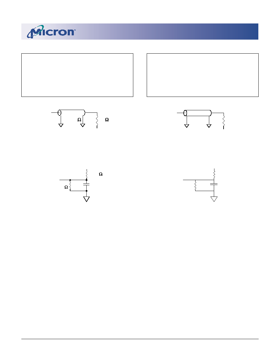
Figure 1
3.3V I/O Output Load Equivalent
Q
351
317
5pF
+3.3V
Figure 2
3.3V I/O Output Load Equivalent
3.3V I/O AC TEST CONDITIONS
Input pulse levels .................. V
IH
= (V
DD
/2.2) + 1.5V
.................... V
IL
= (V
DD
/2.2) - 1.5V
Input rise and fall times ..................................... 1ns
Input timing reference levels ...................... V
DD
/2.2
Output reference levels ............................ V
DD
Q/2.2
Output load ............................. See Figures 1 and 2
LOAD DERATING CURVES
Micron 512K x 18, 256K x 32, and 256K x 36
SyncBurst SRAM timing is dependent upon the capaci-
tive loading on the outputs.
Consult the factory for copies of I/O current versus
voltage curves.
Q
50
V = 1.25V
Z = 50
O
T
Figure 3
2.5V I/O Output Load Equivalent
Q
225
225
5pF
+2.5V
Figure 4
2.5V I/O Output Load Equivalent
2.5V I/O AC TEST CONDITIONS
Input pulse levels .............. V
IH
= (V
DD
/2.64) + 1.25V
................ V
IL
= (V
DD
/2.64) - 1.25V
Input rise and fall times ..................................... 1ns
Input timing reference levels ................... V
DD
/2.64
Output reference levels ............................... V
DD
Q/2
Output load ............................. See Figures 3 and 4
21
8Mb: 512K x 18, 256K x 32/36 Pipelined, SCD SyncBurst SRAM
Micron Technology, Inc., reserves the right to change products or specifications without notice.
MT58L512L18P_C.p65 ≠ Rev. 2/02
©2002, Micron Technology, Inc.
8Mb: 512K x 18, 256K x 32/36
PIPELINED, SCD SYNCBURST SRAM
SNOOZE MODE
SNOOZE MODE is a low-current, "power-down"
mode in which the device is deselected and current is
reduced to I
SB
2Z
. The duration of SNOOZE MODE is
dictated by the length of time ZZ is in a HIGH state.
After the device enters SNOOZE MODE, all inputs
except ZZ become gated inputs and are ignored.
ZZ is an asynchronous, active HIGH input that
causes the device to enter SNOOZE MODE. When ZZ
becomes a logic HIGH, I
SB
2Z
is guaranteed after the
setup time
t
ZZ is met. Any READ or WRITE operation
pending when the device enters SNOOZE MODE is not
guaranteed to complete successfully. Therefore,
SNOOZE MODE must not be initiated until valid pend-
ing operations are completed.
SNOOZE MODE ELECTRICAL CHARACTERISTICS
DESCRIPTION
CONDITIONS
SYMBOL
MIN
MAX
UNITS
NOTES
Current during SNOOZE MODE
ZZ
V
IH
I
SB
2Z
10
mA
ZZ active to input ignored
t
ZZ
2(
t
KC)
ns
1
ZZ inactive to input sampled
t
RZZ
2(
t
KC)
ns
1
ZZ active to snooze current
t
ZZI
2(
t
KC)
ns
1
ZZ inactive to exit snooze current
t
RZZI
0
ns
1
NOTE: 1. This parameter is sampled.
SNOOZE MODE WAVEFORM
t
ZZ
I
SUPPLY
CLK
ZZ
t
RZZ
ALL INPUTS
(except ZZ)
DON'T CARE
I
ISB2Z
t
ZZI
t
RZZI
Outputs (Q)
High-Z
DESELECT or READ Only
22
8Mb: 512K x 18, 256K x 32/36 Pipelined, SCD SyncBurst SRAM
Micron Technology, Inc., reserves the right to change products or specifications without notice.
MT58L512L18P_C.p65 ≠ Rev. 2/02
©2002, Micron Technology, Inc.
8Mb: 512K x 18, 256K x 32/36
PIPELINED, SCD SYNCBURST SRAM
READ TIMING PARAMETERS
-6
-7.5
-10
SYMBOL
MIN
MAX
MIN
MAX
MIN
MAX
UNITS
t
KC
6.0
7.5
10
ns
f
KF
166
133
100
MHz
t
KH
2.3
2.5
3.0
ns
t
KL
2.3
2.5
3.0
ns
t
KQ
3.5
4.0
5.0
ns
t
KQX
1.5
1.5
1.5
ns
t
KQLZ
0
0
1.5
ns
t
KQHZ
3.5
4.2
5.0
ns
t
OEQ
3.5
4.2
5.0
ns
t
OELZ
0
0
0
ns
t
OEHZ
3.5
4.2
4.5
ns
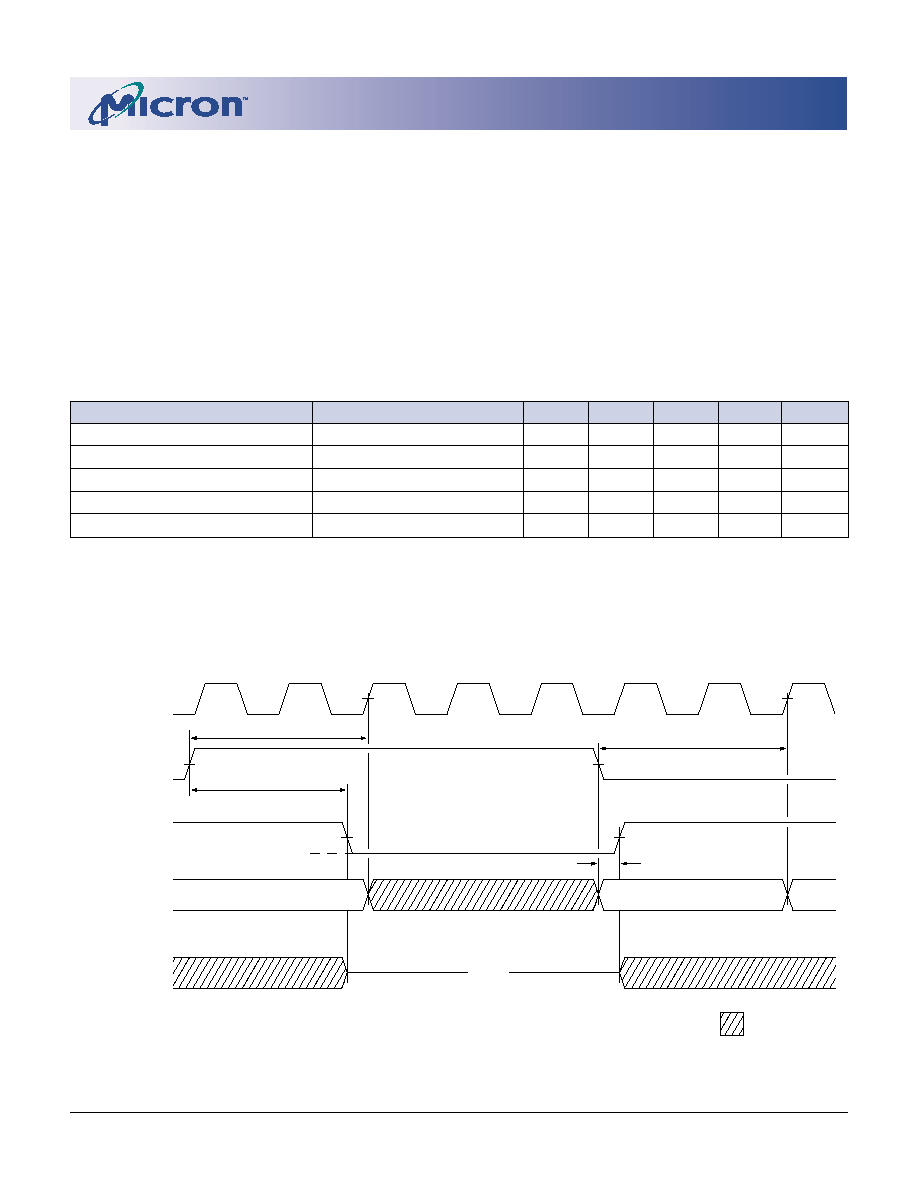
READ TIMING
3
tKC
tKL
CLK
ADSP#
tADSH
tADSS
ADDRESS
tKH
OE#
ADSC#
CE#
(NOTE 2)
tAH
tAS
A1
tCEH
tCES
GW#, BWE#,
BWa#-BWd#
Q
High-Z
tKQLZ
tKQX
tKQ
ADV#
tOEHZ
tKQ
Single READ
BURST READ
tOEQ
tOELZ
tKQHZ
ADV#
suspends
burst.
Burst wraps around
to its initial state.
tAAH
tAAS
tWH
tWS
tADSH
tADSS
Q(A2)
Q(A2 + 1)
Q(A2 + 2)
Q(A1)
Q(A2)
Q(A2 + 1)
Q(A2 + 3)
A2
A3
(NOTE 1)
Deselect
cycle.
(NOTE 3)
(NOTE 4)
Burst continued with
new base address.
DON'T CARE
UNDEFINED
NOTE: 1. Q(A2) refers to output from address A2. Q(A2 + 1) refers to output from the next internal burst address following A2.
2. CE2# and CE2 have timing identical to CE#. On this diagram, when CE# is LOW, CE2# is LOW and CE2 is HIGH. When
CE# is HIGH, CE2# is HIGH and CE2 is LOW.
3. Timing is shown assuming that the device was not enabled before entering into this sequence. OE# does not cause Q
to be driven until after the following clock rising edge.
4. Outputs are disabled within one clock cycle after deselect.
t
AS
1.5
1.5
2.0
ns
t
ADSS
1.5
1.5
2.0
ns
t
AAS
1.5
1.5
2.0
ns
t
WS
1.5
1.5
2.0
ns
t
CES
1.5
1.5
2.0
ns
t
AH
0.5
0.5
0.5
ns
t
ADSH
0.5
0.5
0.5
ns
t
AAH
0.5
0.5
0.5
ns
t
WH
0.5
0.5
0.5
ns
t
CEH
0.5
0.5
0.5
ns
-6
-7.5
-10
SYMBOL
MIN
MAX
MIN
MAX
MIN
MAX
UNITS
23
8Mb: 512K x 18, 256K x 32/36 Pipelined, SCD SyncBurst SRAM
Micron Technology, Inc., reserves the right to change products or specifications without notice.
MT58L512L18P_C.p65 ≠ Rev. 2/02
©2002, Micron Technology, Inc.
8Mb: 512K x 18, 256K x 32/36
PIPELINED, SCD SYNCBURST SRAM
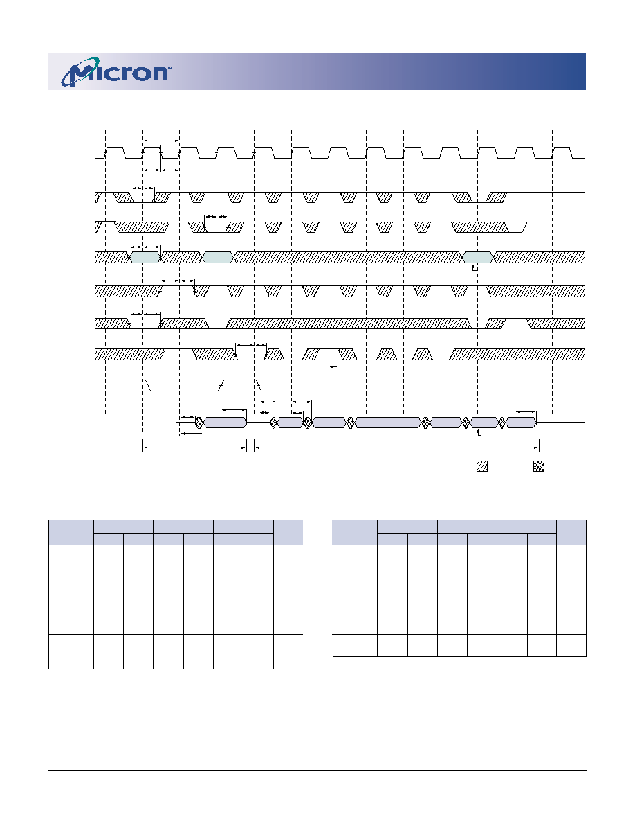
WRITE TIMING
tKC
tKL
CLK
ADSP#
tADSH
tADSS
ADDRESS
tKH
OE#
ADSC#
CE#
(NOTE 2)
tAH
tAS
A1
tCEH
tCES
BWE#,
BWa#-BWd#
Q
High-Z
ADV#
BURST READ
BURST WRITE
D(A2)
D(A2 + 1)
D(A2 + 1)
D(A1)
D(A3)
D(A3 + 1)
D(A3 + 2)
D(A2 + 3)
A2
A3
D
Extended BURST WRITE
D(A2 + 2)
Single WRITE
tADSH
tADSS
tADSH
tADSS
tOEHZ
tAAH
tAAS
tWH
tWS
tDH
tDS
(NOTE 3)
(NOTE 1)
(NOTE 4)
GW#
tWH
tWS
(NOTE 5)
Byte write signals are
ignored for first cycle when
ADSP# initiates burst.
ADSC# extends burst.
ADV# suspends burst.
DON'T CARE
UNDEFINED
NOTE: 1. D(A2) refers to input for address A2. D(A2 + 1) refers to input for the next internal burst address following A2.
2. CE2# and CE2 have timing identical to CE#. On this diagram, when CE# is LOW, CE2# is LOW and CE2 is HIGH.
When CE# is HIGH, CE2# is HIGH and CE2 is LOW.
3. OE# must be HIGH before the input data setup and held HIGH throughout the data hold time. This prevents
input/output data contention for the time period prior to the byte write enable inputs being sampled.
4. ADV# must be HIGH to permit a WRITE to the loaded address.
5. Full-width WRITE can be initiated by GW# LOW; or GW# HIGH and BWE#, BWa# and BWb# LOW for x18 device;
or GW# HIGH and BWE#, BWa#-BWd# LOW for x32 and x36 devices.
t
DS
1.5
1.5
2.0
ns
t
CES
1.5
1.5
2.0
ns
t
AH
0.5
0.5
0.5
ns
t
ADSH
0.5
0.5
0.5
ns
t
AAH
0.5
0.5
0.5
ns
t
WH
0.5
0.5
0.5
ns
t
DH
0.5
0.5
0.5
ns
t
CEH
0.5
0.5
0.5
ns
WRITE TIMING PARAMETERS
-6
-7.5
-10
SYMBOL
MIN
MAX
MIN
MAX
MIN
MAX
UNITS
t
KC
6.0
7.5
10
ns
f
KF
166
133
100
MHz
t
KH
2.3
2.5
3.0
ns
t
KL
2.3
2.5
3.0
ns
t
OEHZ
3.5
4.2
4.5
ns
t
AS
1.5
1.5
2.0
ns
t
ADSS
1.5
1.5
2.0
ns
t
AAS
1.5
1.5
2.0
ns
t
WS
1.5
1.5
2.0
ns
-6
-7.5
-10
SYMBOL
MIN
MAX
MIN
MAX
MIN
MAX
UNITS
24
8Mb: 512K x 18, 256K x 32/36 Pipelined, SCD SyncBurst SRAM
Micron Technology, Inc., reserves the right to change products or specifications without notice.
MT58L512L18P_C.p65 ≠ Rev. 2/02
©2002, Micron Technology, Inc.
8Mb: 512K x 18, 256K x 32/36
PIPELINED, SCD SYNCBURST SRAM
READ/WRITE TIMING
3
tKC
tKL
CLK
ADSP#
tADSH
tADSS
ADDRESS
tKH
OE#
ADSC#
CE#
(NOTE 2)
tAH
tAS
A2
tCEH
tCES
BWE#,
BWa#-BWd#
(NOTE 4)
Q
High-Z
ADV#
Single WRITE
D(A3)
A4
A5
A6
D(A5)
D(A6)
D
BURST READ
Back-to-Back READs
High-Z
Q(A2)
Q(A1)
Q(A4)
Q(A4+1)
Q(A4+2)
tWH
tWS
Q(A4+3)
tOEHZ
tDH
tDS
tOELZ
(NOTE 1)
tKQLZ
tKQ
Back-to-Back
WRITEs
A1
(NOTE 5)
DON'T CARE
UNDEFINED
A3
NOTE: 1. Q(A4) refers to output from address A4. Q(A4 + 1) refers to output from the next internal burst address following A4.
2. CE2# and CE2 have timing identical to CE#. On this diagram, when CE# is LOW, CE2# is LOW and CE2 is HIGH. When
CE# is HIGH, CE2# is HIGH and CE2 is LOW.
3. The data bus (Q) remains in High-Z following a WRITE cycle unless an ADSP#, ADSC# or ADV# cycle is performed.
4. GW# is HIGH.
5. Back-to-back READs may be controlled by either ADSP# or ADSC#.
t
ADSS
1.5
1.5
2.0
ns
t
WS
1.5
1.5
2.0
ns
t
DS
1.5
1.5
2.0
ns
t
CES
1.5
1.5
2.0
ns
t
AH
0.5
0.5
0.5
ns
t
ADSH
0.5
0.5
0.5
ns
t
WH
0.5
0.5
0.5
ns
t
DH
0.5
0.5
0.5
ns
t
CEH
0.5
0.5
0.5
ns
READ/WRITE TIMING PARAMETERS
-6
-7.5
-10
SYMBOL
MIN
MAX
MIN
MAX
MIN
MAX
UNITS
t
KC
6.0
7.5
10
ns
f
KF
166
133
100
MHz
t
KH
2.3
2.5
3.0
ns
t
KL
2.3
2.5
3.0
ns
t
KQ
3.5
4.0
5.0
ns
t
KQLZ
0
0
1.5
ns
t
OELZ
0
0
0
ns
t
OEHZ
3.5
4.2
4.5
ns
t
AS
1.5
1.5
2.0
ns
-6
-7.5
-10
SYMBOL
MIN
MAX
MIN
MAX
MIN
MAX
UNITS
25
8Mb: 512K x 18, 256K x 32/36 Pipelined, SCD SyncBurst SRAM
Micron Technology, Inc., reserves the right to change products or specifications without notice.
MT58L512L18P_C.p65 ≠ Rev. 2/02
©2002, Micron Technology, Inc.
8Mb: 512K x 18, 256K x 32/36
PIPELINED, SCD SYNCBURST SRAM
100-PIN PLASTIC TQFP (JEDEC LQFP)
14.00 ±0.10
20.10 ±0.10
0.62
22.10
+0.10
-0.15
16.00
+0.20
-0.05
PIN #1 ID
0.65
1.50 ±0.10
0.25
0.60 ±0.15
1.40 ±0.05
0.32
+0.06
-0.10
0.15
+0.03
-0.02
0.10
+0.10
-0.05
DETAIL A
DETAIL A
1.00 (TYP)
GAGE PLANE
0.10
NOTE: 1. All dimensions in millimeters MAX or typical where noted.
MIN
2. Package width and length do not include mold protrusion; allowable mold protrusion is 0.01" per side.
26
8Mb: 512K x 18, 256K x 32/36 Pipelined, SCD SyncBurst SRAM
Micron Technology, Inc., reserves the right to change products or specifications without notice.
MT58L512L18P_C.p65 ≠ Rev. 2/02
©2002, Micron Technology, Inc.
8Mb: 512K x 18, 256K x 32/36
PIPELINED, SCD SYNCBURST SRAM
165-PIN FBGA
NOTE: 1. All dimensions in millimeters MAX or typical where noted.
MIN
10.00
14.00
15.00 ±0.10
1.00
TYP
1.00
TYP
5.00 ±0.05
13.00 ±0.10
PIN A1 ID
PIN A1 ID
BALL A1
MOLD COMPOUND: EPOXY NOVOLAC
SUBSTRATE: PLASTIC LAMINATE
6.50 ±0.05
7.00 ±0.05
7.50 ±0.05
1.20 MAX
SOLDER BALL MATERIAL: EUTECTIC 63% Sn, 37% Pb
SOLDER BALL PAD: ÿ .33mm
SOLDER BALL DIAMETER REFERS
TO POST REFLOW CONDITION. THE
PRE-REFLOW DIAMETER IS ÿ 0.40
SEATING PLANE
0.85 ±0.075
0.12 C
C
165X ÿ 0.45
BALL A11
8000 S. Federal Way, P.O. Box 6, Boise, ID 83707-0006, Tel: 208-368-3900
E-mail: prodmktg@micron.com, Internet: http://www.micron.com, Customer Comment Line: 800-932-4992
Micron is a registered trademark and the Micron logo and M logo are trademarks of Micron Technology, Inc.
SyncBurst is a trademark of Micron Technology, Inc.

27
8Mb: 512K x 18, 256K x 32/36 Pipelined, SCD SyncBurst SRAM
Micron Technology, Inc., reserves the right to change products or specifications without notice.
MT58L512L18P_C.p65 ≠ Rev. 2/02
©2002, Micron Technology, Inc.
8Mb: 512K x 18, 256K x 32/36
PIPELINED, SCD SYNCBURST SRAM
REVISION HISTORY
Removed "Preliminary Package Data" from front page ........................................................................ February 22/02
Removed -5 speed grade
Removed 119-pin PBGA package and references .................................................................................. February 14/02
Removed note "Not Recommended for New Designs," Rev. 6/01 ................................................................. June 7/01
Added industrial temperature references and notes, Rev. 3/01 ................................................................ March 19/01
Changed 16Mb references to 18Mb
Changed NC/DQPx to NF/DQPx
Added 119-pin PBGA package, Rev. 1/01, FINAL .................................................................................... January 10/01
Removed FBGA Part Marking Guide, Rev. 8/00, FINAL ............................................................................. August 1/00
Added FBGA Part Marking Guide, Rev 7/00 .................................................................................................. July 18/00
Added Revision History
Removed 119-Pin PBGA package and references
Removed Industrial Temperature references
Added 165-pin FBGA Package ....................................................................................................................... June 13/00