Document Outline
- Features
- Options
- Functional Block Diagrams
- 1 Meg x 18
- 512K x 32/36
- General Description
- Dual Voltage I/O
- TQFP Pin Assignment Table
- Pin Assigment 100-Pin TQFP
- TQFP Pin Descriptions
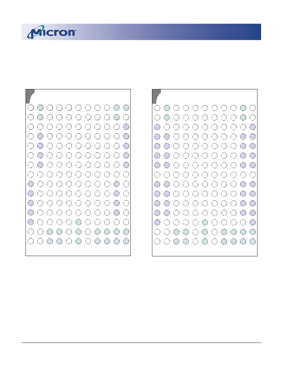
- Pin Layout 165-Pin FBGA
- FBGA Pin Descriptions
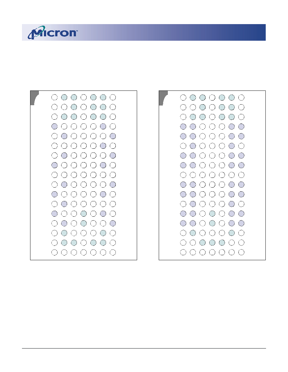
- Pin Layout 119-Pin BGA
- BGA Pin Descriptions
- Interleaved Burst Address Table (Mode = NC or HIGH)
- Linear Burst Address Table (Mode = LOW)
- Partial Truth Table for WRITE Commands (x18)
- Partial Truth Table for WRITE Commands (x32/x36)
- Truth Table
- 3.3V VDD, Absolute Maximum Ratings
- 2.5V VDD, Absolute Maximum Ratings
- 3.3V VDD, 3.3V I/O DC Electrical Characterstics and Operating Conditions
- 3.3V VDD, 2.5V I/O DC Electrical Characteristics and Operating Conditions
- 2.5V VDD, 2.5V I/O DC Electrical Characteristics and Operating Conditions
- TQFP Capacitance
- BGA Capacitance
- FBGA Capacitance
- TQFP Thermal Resistance
- BGA Thermal Resistance
- FBGA Thermal Resistance
- 3.3V VDD, IDD Operating Conditions and Maximum Limits (512K x 32/36)
- 2.5V VDD, IDD Operating Conditions and Maximum Limits (512K x 32/36)
- 3.3V VDD, IDD Operating Conditions and Maximum Limits (1 Meg x 18)
- 2.5V VDD, IDD Operating Conditions and Maximum Limits (1 Meg x 18)
- AC Electrical Characteristics and Recommended Operating Conditions
- 3.3V VDD, 3.3V I/O AC Test Conditions
- 3.3V VDD, 2.5V I/O AC Test Conditions
- 2.5V VDD, 2.5V I/O AC Test Conditions
- Load Derating Curves
- 3.3V I/O Output Load Equivalents
- 2.5V I/O Output Load Equivalents
- Snooze Mode
- Snooze Mode Electrical Characteristics
- Snooze Mode Waveform
- Read Timing
- Write Timing
- Read/Write Timing
- IEEE 1149.1 Serial Boundary Scan (JTAG)
- Disabling the JTAG Feature
- Test Access Port (TAP)
- Test Clock (TCK)
- Test Mode Select (TMS)
- Test Data-In (TDI)
- Test Data-Out (TDO)
- Performing a TAP Reset
- Figure 5 TAP Controller State Diagram
- TAP Registers
- Instruction Register
- Bypass Register
- Boundary Scan Register
- Identification (ID) Register
- Figure 6 TAP Controller Block Diagram
- TAP Instruction Set
- Overview
- EXTEST
- IDCODE
- SAMPLE Z
- SAMPLE/PRELOAD
- BYPASS
- Reserved
- TAP Timing
- TAP AC Electrical Characteristics
- TAP AC Test Conditions
- 3.3V VDD, TAP DC Electrical Characteristics and Operating Conditions
- 2.5V VDD, TAP DC Electrical Characteristics and Operating Conditions
- Figure 7 TAP AC Output Load Equivalent
- Identificaiton Register Definitions
- Scan Register Sizes
- Instruction Codes
- 165-Pin FBGA Boundary Scan Order (x18)
- 165-Pin FBGA Boundary Scan Order (x32)
- 165-Pin FBGA Boundary Scan Order (x36)
- 119-Pin PBGA Boundary Scan Order (x18)
- 119-Pin PBGA Boundary Scan Order (x32)
- 119-Pin PBGA Boundary Scan Order (x36)
- 100-Pin Plastic TQFP (JEDEC LQFP)
- 119-Pin BGA
- 165-Pin FBGA
- Revision History
1
18Mb: 1 Meg x 18, 512K x 32/36 Flow-Through SyncBurst SRAM
©2001, Micron Technology, Inc.
MT58L1MY18F_C.p65 ≠ Rev. C, Pub. 9/01
18Mb: 1 MEG x 18, 512K x 32/36
FLOW-THROUGH SYNCBURST SRAM
ADVANCE
PRODUCTS AND SPECIFICATIONS DISCUSSED HEREIN ARE FOR EVALUATION AND REFERENCE PURPOSES ONLY AND ARE SUBJECT TO CHANGE
BY MICRON WITHOUT NOTICE. PRODUCTS ARE ONLY WARRANTED BY MICRON TO MEET MICRON'S PRODUCTION DATA SHEET SPECIFICATIONS.
18Mb SYNCBURST
TM
SRAM
FEATURES
∑ Fast clock and OE# access times
∑ Single +3.3V ±0.165V or +2.5V ±0.125V power supply
(V
DD
)
∑ Separate +3.3V or +2.5V isolated output buffer supply
(V
DD
Q)
∑ SNOOZE MODE for reduced-power standby
∑ Common data inputs and data outputs
∑ Individual BYTE WRITE control and GLOBAL WRITE
∑ Three chip enables for simple depth expansion and
address pipelining
∑ Clock-controlled and registered addresses, data I/Os,
and control signals
∑ Internally self-timed WRITE cycle
∑ Automatic power-down
∑ Burst control (interleaved or linear burst)
∑ Low capacitive bus loading
∑ x18, x32, and x36 versions available
OPTIONS
TQFP MARKING
∑ Timing (Access/Cycle/MHz)
7.5ns/8.8ns/113 MHz
-7.5
8.5ns/10ns/100 MHz
-8.5
10ns/15ns/66 MHz
-10
∑ Configurations
3.3V V
DD
, 3.3V or 2.5V I/O
1 Meg x 18
MT58L1MY18F
512K x 32
MT58L512Y32F
512K x 36
MT58L512Y36F
2.5V V
DD
, 2.5V I/O
1 Meg x 18
MT58V1MV18F
512K x 32
MT58V512V32F
512K x 36
MT58V512V36F
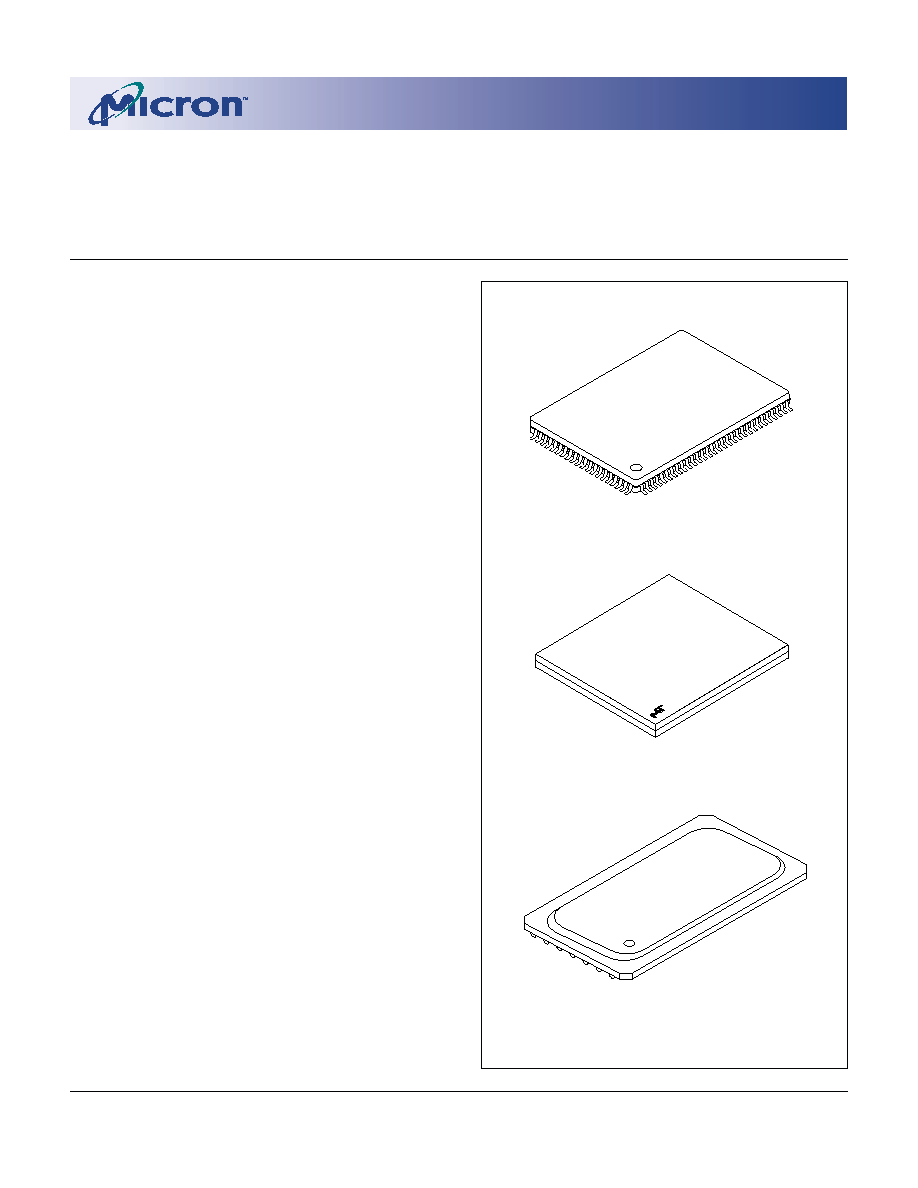
∑ Packages
100-pin TQFP (3-chip enable)
T
165-pin FBGA
F*
119-pin BGA
B
∑ Operating Temperature Range
Commercial (0∫C to +70∫C)
None
Part Number Example:
MT58L512Y36FT-10
MT58L1MY18F, MT58V1MV18F,
MT58L512Y32F, MT58V512V32F,
MT58L512Y36F, MT58V512V36F
3V V
DD
, 3.3V or 2.5V I/O; 2.5V V
DD
, 2.5V
I/O,
Flow-Through
* A Part Marking Guide for the FBGA devices can be found on Micron's
Web site--
http://www.micron.com/support/index.html.
NOTE: 1. JEDEC-standard MS-026 BHA (LQFP).
2. JEDEC-standard MS-028 BHA (PBGA).
119-Pin BGA
2
165-Pin FBGA
100-Pin TQFP
1
2
18Mb: 1 Meg x 18, 512K x 32/36 Flow-Through SyncBurst SRAM
Micron Technology, Inc., reserves the right to change products or specifications without notice.
MT58L1MY18F_C.p65 ≠ Rev. C, Pub. 9/01
©2001, Micron Technology, Inc.
18Mb: 1 MEG x 18, 512K x 32/36
FLOW-THROUGH SYNCBURST SRAM
ADVANCE
FUNCTIONAL BLOCK DIAGRAM
1 MEG x 18
DQs
DQPa
DQPb
ADDRESS
REGISTER
ADV#
CLK
BINARY
COUNTER AND
LOGIC
CLR
Q1
Q0
ADSC#
20
20
18
20
CE#
ENABLE
REGISTER
2
OE#
SENSE
AMPS
1 Meg x 9 x 2
MEMORY
ARRAY
ADSP#
OUTPUT
BUFFERS
INPUT
REGISTERS
2
MODE
CE2
CE2#
GW#
BWE#
SA0, SA1, SAs
BWb#
BWa#
BYTE "b"
WRITE REGISTER
BYTE "a"
WRITE REGISTER
SA0'
SA1'
SA0-SA1
BYTE "b"
WRITE DRIVER
BYTE "a"
WRITE DRIVER
18
18
18
18
9
9
9
9
NOTE: Functional block diagrams illustrate simplified device operation. See truth table, pin description, and timing diagrams for
detailed information.
DQs
DQPa
DQPb
DQPc
DQPd
ADDRESS
REGISTER
ADV#
CLK
BINARY
COUNTER
AND LOGIC
CLR
Q1
Q0
ADSP#
ADSC#
19
19
17
19
CE#
CE2
CE2#
OE#
ENABLE
REGISTER
4
SENSE
AMPS
OUTPUT
BUFFERS
INPUT
REGISTERS
512K x 8 x 4
(x32)
512K x 9 x 4
(x36)
MEMORY
ARRAY
MODE
BWE#
GW#
BWd#
BWc#
BWb#
BWa#
BYTE "d"
WRITE REGISTER
BYTE "c"
WRITE REGISTER
BYTE "b"
WRITE REGISTER
BYTE "a"
WRITE REGISTER
BYTE "b"
WRITE DRIVER
BYTE "c"
WRITE DRIVER
BYTE "d"
WRITE DRIVER
SA0, SA1, SAs
SA0'
SA1'
SA0-SA1
BYTE "a"
WRITE DRIVER
36
36
36
9
9
9
9
9
9
9
9
36
FUNCTIONAL BLOCK DIAGRAM
512K x 32/36

3
18Mb: 1 Meg x 18, 512K x 32/36 Flow-Through SyncBurst SRAM
Micron Technology, Inc., reserves the right to change products or specifications without notice.
MT58L1MY18F_C.p65 ≠ Rev. C, Pub. 9/01
©2001, Micron Technology, Inc.
18Mb: 1 MEG x 18, 512K x 32/36
FLOW-THROUGH SYNCBURST SRAM
ADVANCE
Address and write control are registered on-chip to
simplify WRITE cycles. This allows self-timed WRITE
cycles. Individual byte enables allow individual bytes to
be written. During WRITE cycles on the x18 device, BWa#
controls DQa pins and DQPa; BWb# controls DQb pins
and DQPb. During WRITE cycles on the x32 and x36
devices, BWa# controls DQa pins and DQPa; BWb#
controls DQb pins and DQPb; BWc# controls DQc pins
and DQPc; BWd# controls DQd pins and DQPd. GW#
LOW causes all bytes to be written. Parity bits are only
available on the x18 and x36 versions.
The device is ideally suited for 486, Pentium
Æ
, 680x0
and PowerPC systems and those systems that benefit from
a wide synchronous data bus. The device is also ideal in
generic 16-, 18-, 32-, 36-, 64-, and 72-bit-wide applica-
tions.
Please refer to the Micron Web site (
www.micron.com/
sram
) for the latest data sheet.
DUAL VOLTAGE I/O
The 3.3V V
DD
device is tested for 3.3V and 2.5V I/O
function. The 2.5V V
DD
device is tested for only 2.5V
I/O function.
GENERAL DESCRIPTION
The Micron
Æ
SyncBurst
TM
SRAM family employs high-
speed, low-power CMOS designs that are fabricated using
an advanced CMOS process.
Micron's 18Mb SyncBurst SRAMs integrate a 1 Meg x
18, 512K x 32, or 512K x 36 SRAM core with advanced
synchronous peripheral circuitry and a 2-bit burst counter.
All synchronous inputs pass through registers controlled
by a positive-edge-triggered single-clock input (CLK). The
synchronous inputs include all addresses, all data inputs,
active LOW chip enable (CE#), two additional chip en-
ables for easy depth expansion (CE2#, CE2), burst control
inputs (ADSC#, ADSP#, ADV#), byte write enables (BWx#),
and global write (GW#).
Asynchronous inputs include the output enable (OE#),
clock (CLK) and snooze enable (ZZ). There is also a burst
mode input (MODE) that selects between interleaved and
linear burst modes. The data-out (Q), enabled by OE#, is
also asynchronous. WRITE cycles can be from one to two
bytes wide (x18) or from one to four bytes wide (x32/x36),
as controlled by the write control inputs.
Burst operation can be initiated with either address
status processor (ADSP#) or address status controller
(ADSC#) inputs. Subsequent burst addresses can be in-
ternally generated as controlled by the burst advance
input (ADV#).

4
18Mb: 1 Meg x 18, 512K x 32/36 Flow-Through SyncBurst SRAM
Micron Technology, Inc., reserves the right to change products or specifications without notice.
MT58L1MY18F_C.p65 ≠ Rev. C, Pub. 9/01
©2001, Micron Technology, Inc.
18Mb: 1 MEG x 18, 512K x 32/36
FLOW-THROUGH SYNCBURST SRAM
ADVANCE
NOTE: 1. No Function (NF) is used on the x32 version. Parity (DQPx) is used on the x36 version.
PIN #
x18
x32
x36
51
NC
NF
DQPa
1
52
NC
DQa
DQa
53
NC
DQa
DQa
54
V
DD
Q
55
V
SS
56
NC
DQa
DQa
57
NC
DQa
DQa
58
DQa
59
DQa
60
V
SS
61
V
DD
Q
62
DQa
63
DQa
64
ZZ
65
V
DD
66
NC
67
V
SS
68
DQa
DQb
DQb
69
DQa
DQb
DQb
70
V
DD
Q
71
V
SS
72
DQa
DQb
DQb
73
DQa
DQb
DQb
74
DQPa
DQb
DQb
75
NC
DQb
DQb
PIN #
x18
x32
x36
PIN #
x18
x32
x36
TQFP PIN ASSIGNMENT TABLE
26
V
SS
27
V
DD
Q
28
NC
DQd
DQd
29
NC
DQd
DQd
30
NC
NF
DQPd
1
31
MODE (LBO#)
32
SA
33
SA
34
SA
35
SA
36
SA1
37
SA0
38
DNU
39
DNU
40
V
SS
41
V
DD
42
SA
43
SA
44
SA
45
SA
46
SA
47
SA
48
SA
49
SA
50
SA
PIN #
x18
x32
x36
1
NC
NF
DQPc
1
2
NC
DQc
DQc
3
NC
DQc
DQc
4
V
DD
Q
5
V
SS
6
NC
DQc
DQc
7
NC
DQc
DQc
8
DQb
DQc
DQc
9
DQb
DQc
DQc
10
V
SS
11
V
DD
Q
12
DQb
DQc
DQc
13
DQb
DQc
DQc
14
NC
15
V
DD
16
NC
17
V
SS
18
DQb
DQd
DQd
19
DQb
DQd
DQd
20
V
DD
Q
21
V
SS
22
DQb
DQd
DQd
23
DQb
DQd
DQd
24
DQPb
DQd
DQd
25
NC
DQd
DQd
76
V
SS
77
V
DD
Q
78
NC
DQb
DQb
79
NC
DQb
DQb
80
SA
NF
DQPb
1
81
SA
82
SA
83
ADV#
84
ADSP#
85
ADSC#
86
OE# (G#)
87
BWE#
88
GW#
89
CLK
90
V
SS
91
V
DD
92
CE2#
93
BWa#
94
BWb#
95
NC
BWc# BWc#
96
NC
BWd# BWd#
97
CE2
98
CE#
99
SA
100
SA
5
18Mb: 1 Meg x 18, 512K x 32/36 Flow-Through SyncBurst SRAM
Micron Technology, Inc., reserves the right to change products or specifications without notice.
MT58L1MY18F_C.p65 ≠ Rev. C, Pub. 9/01
©2001, Micron Technology, Inc.
18Mb: 1 MEG x 18, 512K x 32/36
FLOW-THROUGH SYNCBURST SRAM
ADVANCE
SA
SA
ADV#
ADSP#
ADSC#
OE# (G#)
BWE#
GW#
CLK
V
SS
V
DD
CE2#
BWa#
BWb#
NC
NC
CE2
CE#
SA
SA
81
82
83
84
85
86
87
88
89
90
91
92
93
94
95
96
97
98
99
100
50
49
48
47
46
45
44
43
42
41
40
39
38
37
36
35
34
33
32
31
80 79 78 77 76 75 74 73 72 71 70 69 68 67 66 65 64 63 62 61 60 59 58 57 56 55 54 53 52 51
1 2 3 4 5 6 7 8 9 10 11 12 13 14 15 16 17 18 19 20 21 22 23 24 25 26 27 28 29 30
SA
NC
NC
V
DD
Q
V
SS
NC
DQPa
DQa
DQa
V
SS
V
DD
Q
DQa
DQa
V
SS
NC
V
DD
ZZ
DQa
DQa
V
DD
Q
V
SS
DQa
DQa
NC
NC
V
SS
V
DD
Q
NC
NC
NC
SA
SA
SA
SA
SA
SA
SA
SA
SA
V
DD
V
SS
DNU
DNU
SA0
SA1
SA
SA
SA
SA
MODE
(LBO#)
NC
NC
NC
V
DD
Q
V
SS
NC
NC
DQb
DQb
V
SS
V
DD
Q
DQb
DQb
NC
V
DD
NC
V
SS
DQb
DQb
V
DD
Q
V
SS
DQb
DQb
DQPb
NC
V
SS
V
DD
Q
NC
NC
NC
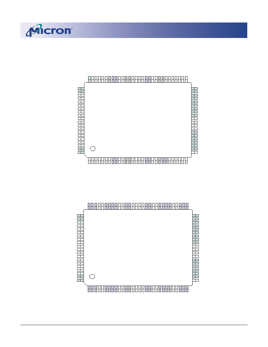
x18
PIN ASSIGNMENT (TOP VIEW)
100-PIN TQFP
NOTE: 1. No Function (NF) is used on the x32 version. Parity (DQPx) is used on the x36 version.
SA
SA
ADV#
ADSP#
ADSC#
OE# (G#)
BWE#
GW#
CLK
V
SS
V
DD
CE2#
BWa#
BWb#
BWc#
BWd#
CE2
CE#
SA
SA
81
82
83
84
85
86
87
88
89
90
91
92
93
94
95
96
97
98
99
100
50
49
48
47
46
45
44
43
42
41
40
39
38
37
36
35
34
33
32
31
80 79 78 77 76 75 74 73 72 71 70 69 68 67 66 65 64 63 62 61 60 59 58 57 56 55 54 53 52 51
1 2 3 4 5 6 7 8 9 10 11 12 13 14 15 16 17 18 19 20 21 22 23 24 25 26 27 28 29 30
NF/
DQPb
1
DQb
DQb
V
DD
Q
V
SS
DQb
DQb
DQb
DQb
V
SS
V
DD
Q
DQb
DQb
V
SS
NC
V
DD
ZZ
DQa
DQa
V
DD
Q
V
SS
DQa
DQa
DQa
DQa
V
SS
V
DD
Q
DQa
DQa
NF/
DQPa
1
SA
SA
SA
SA
SA
SA
SA
SA
SA
V
DD
V
SS
DNU
DNU
SA0
SA1
SA
SA
SA
SA
MODE
(LBO#)
NF/
DQPc
1
DQc
DQc
V
DD
Q
V
SS
DQc
DQc
DQc
DQc
V
SS
V
DD
Q
DQc
DQc
NC
V
DD
NC
V
SS
DQd
DQd
V
DD
Q
V
SS
DQd
DQd
DQd
DQd
V
SS
V
DD
Q
DQd
DQd
NF/
DQPd
1
x32/x36
6
18Mb: 1 Meg x 18, 512K x 32/36 Flow-Through SyncBurst SRAM
Micron Technology, Inc., reserves the right to change products or specifications without notice.
MT58L1MY18F_C.p65 ≠ Rev. C, Pub. 9/01
©2001, Micron Technology, Inc.
18Mb: 1 MEG x 18, 512K x 32/36
FLOW-THROUGH SYNCBURST SRAM
ADVANCE
TQFP PIN DESCRIPTIONS
x18
x32/x36
SYMBOL
TYPE
DESCRIPTION
37
37
SA0
Input
Synchronous Address Inputs: These inputs are registered and must
36
36
SA1
meet the setup and hold times around the rising edge of CLK.
32-35, 42-50,
32-35, 42-50,
SA
80-82, 99,
81, 82, 99,
100
100
93
93
BWa#
Input
Synchronous Byte Write Enables: These active LOW inputs allow
94
94
BWb#
individual bytes to be written and must meet the setup and hold
≠
95
BWc#
times around the rising edge of CLK. A byte write enable is LOW
≠
96
BWd#
for a WRITE cycle and HIGH for a READ cycle. For the x18 version,
BWa# controls DQa pins and DQPa; BWb# controls DQb pins and
DQPb. For the x32 and x36 versions, BWa# controls DQa pins and
DQPa; BWb# controls DQb pins and DQPb; BWc# controls DQc pins
and DQPc; BWd# controls DQd pins and DQPd. Parity is only
available on the x18 and x36 versions.
87
87
BWE#
Input
Byte Write Enable: This active LOW input permits BYTE WRITE
operations and must meet the setup and hold times around the
rising edge of CLK.
88
88
GW#
Input
Global Write: This active LOW input allows a full 18-, 32-, or 36-bit
WRITE to occur independent of the BWE# and BWx# lines and must
meet the setup and hold times around the rising edge of CLK.
89
89
CLK
Input
Clock: CLK registers address, data, chip enable, byte write enables,
and burst control inputs on its rising edge. All synchronous inputs
must meet setup and hold times around the clock's rising edge.
98
98
CE#
Input
Synchronous Chip Enable: This active LOW input is used to enable
the device and conditions the internal use of ADSP#. CE# is sampled
only when a new external address is loaded.
92
92
CE2#
Input
Synchronous Chip Enable: This active LOW input is used to enable
the device and is sampled only when a new external address is
loaded.
97
97
CE2
Input
Synchronous Chip Enable: This active HIGH input is used to enable
the device and is sampled only when a new external address is
loaded.
86
86
OE#
Input
Output Enable: This
active LOW, asynchronous input enables the
(G#)
data I/O output drivers. G# is the JEDEC-standard term for OE#.
83
83
ADV#
Input
Synchronous Address Advance: This active LOW input is used to
advance the internal burst counter, controlling burst access after the
external address is loaded. A HIGH on this pin effectively causes wait
states to be generated (no address advance). To ensure use of
correct address during a WRITE cycle, ADV# must be HIGH at the
rising edge of the first clock after an ADSP# cycle is initiated.
85
85
ADSC#
Input
Synchronous Address Status Controller: This active LOW input
interrupts any ongoing burst, causing a new external address to be
registered. A READ or WRITE is performed using the new address if
CE# is LOW. ADSC# is also used to place the chip into power-down
state when CE# is HIGH.
(continued on next page)

7
18Mb: 1 Meg x 18, 512K x 32/36 Flow-Through SyncBurst SRAM
Micron Technology, Inc., reserves the right to change products or specifications without notice.
MT58L1MY18F_C.p65 ≠ Rev. C, Pub. 9/01
©2001, Micron Technology, Inc.
18Mb: 1 MEG x 18, 512K x 32/36
FLOW-THROUGH SYNCBURST SRAM
ADVANCE
TQFP PIN DESCRIPTIONS (continued)
x18
x32/x36
SYMBOL
TYPE
DESCRIPTION
84
84
ADSP#
Input
Synchronous Address Status Processor: This active LOW input
interrupts any ongoing burst, causing a new external address to be
registered. A READ is performed using the new address,
independent of the byte write enables and ADSC#, but dependent
upon CE#, CE2, and CE2#. ADSP# is ignored if CE# is HIGH. Power-
down state is entered if CE2 is LOW or CE2# is HIGH.
31
31
MODE
Input
Mode: This input selects the burst sequence. A LOW on this pin
(LBO#)
selects "linear burst." NC or HIGH on this pin selects "interleaved
burst." Do not alter input state while device is operating. LBO# is
the JEDEC-standard term for MODE.
64
64
ZZ
Input
Snooze Enable: This active HIGH, asynchronous input causes the
device to enter a low-power standby mode in which all data in the
memory array is retained. When ZZ is active, all other inputs are
ignored. This pin has an internal pull-down and can be floating.
(a)
58, 59,
(a)
52, 53,
DQa
Input/ SRAM Data I/Os: For the x18 version, Byte "a" is associated with DQa
62, 63, 68, 69, 56-59, 62, 63
Output pins; Byte "b" is associated with DQb pins. For the x32 and x36
72, 73
versions, Byte "a" is associated with DQa pins; Byte "b" is associated
(b)
8, 9, 12,
(b)
68, 69,
DQb
with DQb pins; Byte "c" is associated with DQc pins; Byte "d" is
13, 18, 19,
72-75, 78, 79
associated with DQd pins. Input data must meet setup and hold
22, 23
times around the rising edge of CLK.
(c)
2, 3, 6-9,
DQc
12, 13
(d)
18, 19,
DQd
22-25, 28, 29
74
51
NF/
DQPa
NC/
No Function /Parity Data I/Os: On the x32 version, these pins are No
24
80
NF/
DQPb
I/O
Function (NF). On the x18 version, Byte "a" parity is DQPa; Byte "b"
≠
1
NF/
DQPc
parity is DQPb. On the x36 version, Byte "a" parity is DQPa; Byte "b"
≠
30
NF/
DQPd
parity is DQPb; Byte "c" parity is DQPc; Byte "d" parity is DQPd.
No function pins are internally connected to the die and have the
capacitance of an input pin. It is allowable to leave these pins
unconnected or driven by signals.
15, 41, 65, 91 15, 41, 65, 91
V
DD
Supply Power Supply:
See DC Electrical Characteristics and Operating
Conditions for range.
4, 11, 20, 27,
4, 11, 20, 27,
V
DD
Q
Supply Isolated Output Buffer Supply: See DC Electrical Characteristics and
54, 61, 70, 77 54, 61, 70, 77
Operating Conditions for range.
5, 10, 17,
5, 10, 17,
V
SS
Supply Ground:
GND.
21, 26, 40,
21, 26, 40,
55,60, 67,
55, 60, 67,
71, 76, 90
71, 76, 90
38, 39
38, 39
DNU
≠
Do Not Use: These signals may either be unconnected or wired to
GND to improve package heat dissipation.
1-3, 6, 7, 14,
14, 16, 66
NC
≠
No Connect: These signals are not internally connected and may be
16, 25, 28-30,
connected to ground to improve package heat dissipation.
51-53, 56, 57,
66, 75, 78, 79,
95, 96
8
18Mb: 1 Meg x 18, 512K x 32/36 Flow-Through SyncBurst SRAM
Micron Technology, Inc., reserves the right to change products or specifications without notice.
MT58L1MY18F_C.p65 ≠ Rev. C, Pub. 9/01
©2001, Micron Technology, Inc.
18Mb: 1 MEG x 18, 512K x 32/36
FLOW-THROUGH SYNCBURST SRAM
ADVANCE
PIN LAYOUT (TOP VIEW)
165-PIN FBGA
A
B
C
D
E
F
G
H
J
K
L
M
N
P
R
A
B
C
D
E
F
G
H
J
K
L
M
N
P
R
2
CE#
CE2
V
DD
Q
V
DD
Q
V
DD
Q
V
DD
Q
V
DD
Q
NC
V
DD
Q
V
DD
Q
V
DD
Q
V
DD
Q
V
DD
Q
SA
SA
SA
SA
NC
DQb
DQb
DQb
DQb
V
SS
NC
NC
NC
NC
NC
NC
NC
NC
NC
NC
NC
NC
NC
NC
V
SS
DQb
DQb
DQb
DQb
DQPb
NC
MODE
(LBO#)
BWb#
NC
V
SS
V
DD
V
DD
V
DD
V
DD
V
DD
V
DD
V
DD
V
DD
V
DD
V
SS
SA
SA
NC
BWa#
V
SS
V
SS
V
SS
V
SS
V
SS
V
SS
V
SS
V
SS
V
SS
V
SS
NC
TD1
TMS
CE2#
CLK
V
SS
V
SS
V
SS
V
SS
V
SS
V
SS
V
SS
V
SS
V
SS
V
SS
SA
SA1
SA0
BWE#
GW#
V
SS
V
SS
V
SS
V
SS
V
SS
V
SS
V
SS
V
SS
V
SS
V
SS
V
SS
TD0
TCK
ADSC#
OE# (G#)
V
SS
V
DD
V
DD
V
DD
V
DD
V
DD
V
DD
V
DD
V
DD
V
DD
V
SS
SA
SA
ADV#
ADSP#
V
DD
Q
V
DD
Q
V
DD
Q
V
DD
Q
V
DD
Q
NC
V
DD
Q
V
DD
Q
V
DD
Q
V
DD
Q
V
DD
Q
SA
SA
SA
SA
NC
NC
NC
NC
NC
NC
DQa
DQa
DQa
DQa
NC
SA
SA
SA
NC
DQPa
DQa
DQa
DQa
DQa
ZZ
NC
NC
NC
NC
NC
SA
SA
TOP VIEW
3
4
5
6
7
8
9
10
11
1
A
B
C
D
E
F
G
H
J
K
L
M
N
P
R
A
B
C
D
E
F
G
H
J
K
L
M
N
P
R
2
CE#
CE2
V
DD
Q
V
DD
Q
V
DD
Q
V
DD
Q
V
DD
Q
NC
V
DD
Q
V
DD
Q
V
DD
Q
V
DD
Q
V
DD
Q
SA
SA
SA
SA
NC
DQc
DQc
DQc
DQc
V
SS
DQd
DQd
DQd
DQd
NC
NC
NC
NC
NC
NF/
DQPc
DQc
DQc
DQc
DQc
V
SS
DQd
DQd
DQd
DQd
NF/
DQPd
NC
MODE
(LBO#)
BWc#
BWd#
V
SS
V
DD
V
DD
V
DD
V
DD
V
DD
V
DD
V
DD
V
DD
V
DD
V
SS
SA
SA
BWb#
BWa#
V
SS
V
SS
V
SS
V
SS
V
SS
V
SS
V
SS
V
SS
V
SS
V
SS
NC
TD1
TMS
CE2#
CLK
V
SS
V
SS
V
SS
V
SS
V
SS
V
SS
V
SS
V
SS
V
SS
V
SS
SA
SA1
SA0
BWE#
GW#
V
SS
V
SS
V
SS
V
SS
V
SS
V
SS
V
SS
V
SS
V
SS
V
SS
V
SS
TD0
TCK
ADSC#
OE# (G#)
V
SS
V
DD
V
DD
V
DD
V
DD
V
DD
V
DD
V
DD
V
DD
V
DD
V
SS
SA
SA
ADV#
ADSP#
V
DD
Q
V
DD
Q
V
DD
Q
V
DD
Q
V
DD
Q
NC
V
DD
Q
V
DD
Q
V
DD
Q
V
DD
Q
V
DD
Q
SA
SA
SA
SA
NC
DQb
DQb
DQb
DQb
NC
DQa
DQa
DQa
DQa
NC
SA
SA
NC
NC
NF/
DQPb
DQb
DQb
DQb
DQb
ZZ
DQa
DQa
DQa
DQa
NF/
DQPa
SA
SA
TOP VIEW
3
4
5
6
7
8
9
10
11
1
x18
x32/x36
NOTE: 1. No Function (NF) is used on the x32 version. Parity (DQPx) is used on the x36 version.

9
18Mb: 1 Meg x 18, 512K x 32/36 Flow-Through SyncBurst SRAM
Micron Technology, Inc., reserves the right to change products or specifications without notice.
MT58L1MY18F_C.p65 ≠ Rev. C, Pub. 9/01
©2001, Micron Technology, Inc.
18Mb: 1 MEG x 18, 512K x 32/36
FLOW-THROUGH SYNCBURST SRAM
ADVANCE
FBGA PIN DESCRIPTIONS
x18
x32/x36
SYMBOL
TYPE
DESCRIPTION
6R
6R
SA0
Input
Synchronous Address Inputs: These inputs are registered and must
6P
6P
SA1
meet the setup and hold times around the rising edge of CLK.
2A, 2B, 3P,
2A, 2B, 3P,
SA
3R, 4P, 4R, 6N, 3R, 4P, 4R, 6N,
8P, 8R, 9P, 9R,
8P, 8R, 9P,
10A, 10B, 10P, 9R, 10A, 10B,
10R, 11A, 11P, 10P, 10R, 11P,
11R
11R
5B
5B
BWa#
Input
Synchronous Byte Write Enables: These active LOW inputs allow
4A
5A
BWb#
individual bytes to be written and must meet the setup and hold
≠
4A
BWc#
times around the rising edge of CLK. A byte write enable is LOW
≠
4B
BWd#
for a WRITE cycle and HIGH for a READ cycle. For the x18 version,
BWa# controls DQa pins and DQPa; BWb# controls DQb pins and
DQPb. For the x32 and x36 versions, BWa# controls DQa pins and
DQPa; BWb# controls DQb pins and DQPb; BWc# controls DQc pins
and DQPc; BWd# controls DQd pins and DQPd. Parity is only
available on the x18 and x36 versions.
7A
7A
BWE#
Input
Byte Write Enable: This active LOW input permits BYTE WRITE
operations and must meet the setup and hold times around the
rising edge of CLK.
7B
7B
GW#
Input
Global Write: This active LOW input allows a full 18-, 32-, or 36-bit
WRITE to occur independent of the BWE# and BWx# lines and must
meet the setup and hold times around the rising edge of CLK.
6B
6B
CLK
Input
Clock: This signal registers the address, data, chip enable, byte write
enables, and burst control inputs on its rising edge. All synchronous
inputs must meet setup and hold times around the clock's rising
edge.
3A
3A
CE#
Input
Synchronous Chip Enable: This active LOW input is used to enable
the device and conditions the internal use of ADSP#. CE# is sampled
only when a new external address is loaded.
6A
6A
CE2#
Input
Synchronous Chip Enable: This active LOW input is used to enable
the device and is sampled only when a new external address is
loaded.
11H
11H
ZZ
Input
Snooze Enable: This active HIGH, asynchronous input causes the
device to enter a low-power standby mode in which all data in the
memory array is retained. When ZZ is active, all other inputs are
ignored.
3B
3B
CE2
Input
Synchronous Chip Enable: This active HIGH input is used to enable
the device and is sampled only when a new external address is
loaded.
8B
8B
OE#(G#)
Input
Output Enable: This
active LOW, asynchronous input enables the
data I/O output drivers.
(continued on next page)

10
18Mb: 1 Meg x 18, 512K x 32/36 Flow-Through SyncBurst SRAM
Micron Technology, Inc., reserves the right to change products or specifications without notice.
MT58L1MY18F_C.p65 ≠ Rev. C, Pub. 9/01
©2001, Micron Technology, Inc.
18Mb: 1 MEG x 18, 512K x 32/36
FLOW-THROUGH SYNCBURST SRAM
ADVANCE
FBGA PIN DESCRIPTIONS (continued)
x18
x32/x36
SYMBOL
TYPE
DESCRIPTION
9A
9A
ADV#
Input
Synchronous Address Advance: This active LOW input is used to
advance the internal burst counter, controlling burst access after the
external address is loaded. A HIGH on ADV# effectively causes wait
states to be generated (no address advance). To ensure use of
correct address during a WRITE cycle, ADV# must be HIGH at the
rising edge of the first clock after an ADSP# cycle is initiated.
9B
9B
ADSP#
Input
Synchronous Address Status Processor: This active LOW input
interrupts any ongoing burst, causing a new external address to be
registered. A READ is performed using the new address,
independent of the byte write enables and ADSC#, but dependent
upon CE#, CE2 and CE2#. ADSP# is ignored if CE# is HIGH. Power-
down state is entered if CE2 is LOW or CE2# is HIGH.
8A
8A
ADSC#
Input
Synchronous Address Status Controller: This active LOW input
interrupts any ongoing burst, causing a new external address to be
registered. A READ or WRITE is performed using the new address if
CE# is LOW. ADSC# is also used to place the chip into power-down
state when CE# is HIGH.
1R
1R
MODE
Input
Mode: This input selects the burst sequence. A LOW on this
(LB0#)
input selects "linear burst." NC or HIGH on this input selects
"interleaved burst." Do not alter input state while device is
operating.
5R
5R
TMS
Input
IEEE 1149.1 Test Inputs: JEDEC-standard 2.5V I/O levels. These pins
5P
5P
TDI
may be left not connected if the JTAG function is not used in the
7R
7R
TCK
circuit.
(a)
10J, 10K,
(a)
10J, 10K,
DQa
Input/ SRAM Data I/Os: For the x18 version, Byte "a" is associated with DQa
10L, 10M, 11D, 10L, 10M, 11J,
Output pins; Byte "b" is associated with DQb pins. For the x32 and x36
11E, 11F, 11G 11K, 11L, 11M
versions, Byte "a" is associated with DQa pins; Byte "b" is associated
(b)
1J, 1K,
(b)
10D, 10E,
DQb
with DQb pins; Byte "c" is associated with DQc pins; Byte "d" is
1L, 1M, 2D,
10F, 10G, 11D,
associated with DQd pins. Input data must meet setup and hold
2E, 2F, 2G
11E, 11F, 11G
times around the rising edge of CLK.
(c)
1D, 1E,
DQc
1F, 1G, 2D,
2E, 2F, 2G
(d)
1J, 1K, 1L,
DQd
1M, 2J, 2K,
2L, 2M
11C
11N
NF/
DQPa
NF/
No Function/Parity Data I/Os: On the x32 version, these are no
1N
11C
NF/
DQPb
I/O
function (NF). On the x18 version, Byte "a" parity is DQPa; Byte "b"
≠
1C
NF/
DQPc
parity is DQPb. On the x36 version, Byte "a" parity is DQPa; Byte
≠
1N
NF/
DQPd
"b" parity is DQPb; Byte "c" parity is DQPc; Byte "d" parity is DQPd.
No function pins are internally connected to the die and have the
capacitance of an input pin. It is allowable to leave these pins
unconnected or driven by signals.
(continued on next page)
11
18Mb: 1 Meg x 18, 512K x 32/36 Flow-Through SyncBurst SRAM
Micron Technology, Inc., reserves the right to change products or specifications without notice.
MT58L1MY18F_C.p65 ≠ Rev. C, Pub. 9/01
©2001, Micron Technology, Inc.
18Mb: 1 MEG x 18, 512K x 32/36
FLOW-THROUGH SYNCBURST SRAM
ADVANCE
FBGA PIN DESCRIPTIONS (continued)
x18
x32/x36
SYMBOL
TYPE
DESCRIPTION
4D, 4E, 4F,
4D, 4E, 4F,
V
DD
Supply Power Supply:
See DC Electrical Characteristics and Operating
4G, 4H, 4J,
4G, 4H, 4J,
Conditions for range.
4K, 4L, 4M,
4K, 4L, 4M,
8D, 8E, 8F,
8D, 8E, 8F,
8G, 8H, 8J,
8G, 8H, 8J,
8K, 8L, 8M
8K, 8L, 8M
3C, 3D, 3E,
3C, 3D, 3E,
V
DD
Q
Supply Isolated Output Buffer Supply: See DC Electrical Characteristics and
3F, 3G, 3J,
3F, 3G, 3J,
Operating Conditions for range.
3K, 3L, 3M,
3K, 3L, 3M,
3N, 9C, 9D,
3N, 9C, 9D,
9E, 9F, 9G,
9E, 9F, 9G,
9J, 9K, 9L,
9J, 9K, 9L,
9M, 9N
9M, 9N
1H, 2H, 4C, 4N, 1H, 2H, 4C, 4N,
V
SS
Supply Ground:
GND.
5C, 5D, 5E 5F, 5C, 5D, 5E 5F,
5G, 5H, 5J, 5K, 5G, 5H, 5J, 5K,
5L, 5M, 6C, 6D, 5L, 5M, 6C, 6D,
6E, 6F, 6G, 6H, 6E, 6F, 6G, 6H,
6J, 6K, 6L, 6M, 6J, 6K, 6L, 6M,
7C, 7D, 7E, 7F, 7C, 7D, 7E, 7F,
7G, 7H, 7J,
7G, 7H, 7J,
7K, 7L, 7M,
7K, 7L, 7M,
7N, 8C, 8N
7N, 8C, 8N
7P
7P
TDO
Output IEEE 1149.1 Test Outputs: JEDEC-standard 2.5V I/O level.
1A, 1B, 1C,
1A, 1B, 1P,
NC
≠
No Connect: These signals are not internally connected and
1D, 1E, 1F,
2C, 2N,
may be connected to ground to improve package heat
1G, 1P, 2C,
2P, 2R, 3H,
dissipation.
2J, 2K, 2L,
5N, 9H, 10C,
2M, 2N, 2P,
10H, 10N,
2R, 3H, 4B,
11A, 11B
5A, 5N, 9H,
10C, 10D,
10E, 10F,
10G, 10H,
10N, 11B,
11J, 11K,
11L, 11M,
11N
12
18Mb: 1 Meg x 18, 512K x 32/36 Flow-Through SyncBurst SRAM
Micron Technology, Inc., reserves the right to change products or specifications without notice.
MT58L1MY18F_C.p65 ≠ Rev. C, Pub. 9/01
©2001, Micron Technology, Inc.
18Mb: 1 MEG x 18, 512K x 32/36
FLOW-THROUGH SYNCBURST SRAM
ADVANCE
PIN LAYOUT (TOP VIEW)
119-PIN BGA
x18
x32/x36
NOTE: 1. No Function (NF) is used on the x32 version. Parity (DQPx) is used on the x36 version.
A
B
C
D
E
F
G
H
J
K
L
M
N
P
R
T
U
1
V
DD
Q
NC
NC
DQc
DQc
V
DD
Q
DQc
DQc
V
DD
Q
DQd
DQd
V
DD
Q
DQd
DQd
NC
NC
V
DD
Q
SA
SA
SA
NF/
DQPc
1
DQc
DQc
DQc
DQc
V
DD
DQd
DQd
DQd
DQd
NF/
DQPd
1
SA
NC
TMS
SA
SA
SA
V
SS
V
SS
V
SS
BWc#
V
SS
NC
V
SS
BWd#
V
SS
V
SS
V
SS
MODE (LBO#)
SA
TDI
ADSP#
ADSC#
V
DD
NC
CE#
OE#
ADV#
GW#
V
DD
CLK
NC
BWE#
SA1
SA0
V
DD
SA
TCK
SA
SA
SA
V
SS
V
SS
V
SS
BWb#
V
SS
NC
V
SS
BWa#
V
SS
V
SS
V
SS
V
DD
SA
TCO
SA
SA
SA
NF/
DQPb
1
DQb
DQb
DQb
DQb
V
DD
DQa
DQa
DQa
DQa
NF/
DQPa
1
SA
NC
NC
V
DD
Q
NC
NC
DQb
DQb
V
DD
Q
DQb
DQb
V
DD
Q
DQa
DQa
V
DD
Q
DQa
DQa
NC
ZZ
V
DD
Q
TOP VIEW
2
3
4
5
6
7
A
B
C
D
E
F
G
H
J
K
L
M
N
P
R
T
U
1
V
DD
Q
NC
NC
DQb
NC
V
DD
Q
NC
DQb
V
DD
Q
NC
DQb
V
DD
Q
DQb
NC
NC
NC
V
DD
Q
SA
SA
SA
NC
DQb
NC
DQb
NC
V
DD
DQb
NC
DQb
NC
DQPb
SA
SA
TMS
SA
SA
SA
V
SS
V
SS
V
SS
BWb#
V
SS
NC
V
SS
V
SS
V
SS
V
SS
V
SS
MODE (LBO#)
SA
TDI
ADSP#
ADSC#
V
DD
NC
CE#
OE#
ADV#
GW#
V
DD
CLK
NC
BWE#
SA1
SA0
V
DD
NC
TCK
SA
SA
SA
V
SS
V
SS
V
SS
V
SS
V
SS
NC
V
SS
BWa#
V
SS
V
SS
V
SS
V
DD
SA
TDO
SA
SA
SA
DQPa
NC
DQa
NC
DQa
V
DD
NC
DQa
NC
DQa
NC
SA
SA
NC
V
DD
Q
NC
NC
NC
DQa
V
DD
Q
DQa
NC
V
DD
Q
DQa
NC
V
DD
Q
NC
DQa
NC
ZZ
V
DD
Q
TOP VIEW
2
3
4
5
6
7
13
18Mb: 1 Meg x 18, 512K x 32/36 Flow-Through SyncBurst SRAM
Micron Technology, Inc., reserves the right to change products or specifications without notice.
MT58L1MY18F_C.p65 ≠ Rev. C, Pub. 9/01
©2001, Micron Technology, Inc.
18Mb: 1 MEG x 18, 512K x 32/36
FLOW-THROUGH SYNCBURST SRAM
ADVANCE
BGA PIN DESCRIPTIONS
x18
x32/x36
SYMBOL
TYPE
DESCRIPTION
4P
4P
SA0
Input
Synchronous Address Inputs: These inputs are registered and must
4N
4N
SA1
meet the setup and hold times around the rising edge of CLK.
2A, 3A, 5A,
2A, 3A, 5A,
SA
6A, 2B, 3B,
6A, 2B, 3B,
5B, 6B, 2C,
5B, 6B, 2C,
3C, 5C, 6C,
3C, 5C, 6C,
2R, 6R, 2T,
2R, 6R, 3T,
3T, 5T, 6T
4T, 5T
5L
5L
BWa#
Input
Synchronous Byte Write Enables: These active LOW inputs allow
3G
5G
BWb#
individual bytes to be written and must meet the setup and hold
≠
3G
BWc#
times around the rising edge of CLK. A byte write enable is LOW
≠
3L
BWd#
for a WRITE cycle and HIGH for a READ cycle. For the x18 version,
BWa# controls DQ pins and DQPa; BWb# controls DQb pins and
DQPb. For the x32 and x36 versions, BWa# controls DQa pins and
DQPa; BWb# controls DQb pins and DQPb; BWc# controls DQc pins
and DQPc; BWd# controls DQd pins and DQPd.
4M
4M
BWE#
Input
Byte Write Enable: This active LOW input permits BYTE WRITE
operations and must meet the setup and hold times around the
rising edge of CLK.
4H
4H
GW#
Input
Global Write: This active LOW input allows a full 18-, 32-, or 36-bit
WRITE to occur independent of the BWE# and BWx# lines and must
meet the setup and hold times around the rising edge of CLK.
4K
4K
CLK
Input
Clock: This signal registers the address, data, chip enable, byte write
enables and burst control inputs on its rising edge. All synchronous
inputs must meet setup and hold times around the clock's rising
edge.
4E
4E
CE#
Input
Synchronous Chip Enable: This active LOW input is used to enable
the device and conditions the internal use of ADSP#. CE# is sampled
only when a new external address is loaded.
7T
7T
ZZ
Input
Snooze Enable: This active HIGH, asynchronous input causes the
device to enter a low-power standby mode in which all data in the
memory array is retained. When ZZ is active, all other inputs are
ignored.
4F
4F
OE#
Input
Output Enable: This
active LOW, asynchronous input enables the
(G#)
data I/O output drivers. G# is the JEDEC-standard term for OE#.
4G
4G
ADV#
Input
Synchronous Address Advance: This active LOW input is used to
advance the internal burst counter, controlling burst access after the
external address is loaded. A HIGH on ADV# effectively causes wait
states to be generated (no address advance). To ensure use of
correct address during a WRITE cycle, ADV# must be HIGH at the
rising edge of the first clock after an ADSP# cycle is initiated.
2U
2U
TMS
Input
IEEE 1149.1 test inputs: JEDEC-standard 2.5V I/O levels. These pins
3U
3U
TDI
may be left Not Connected if the JTAG function is not used in the
4U
4U
TCK
circuit.
(continued on next page)

14
18Mb: 1 Meg x 18, 512K x 32/36 Flow-Through SyncBurst SRAM
Micron Technology, Inc., reserves the right to change products or specifications without notice.
MT58L1MY18F_C.p65 ≠ Rev. C, Pub. 9/01
©2001, Micron Technology, Inc.
18Mb: 1 MEG x 18, 512K x 32/36
FLOW-THROUGH SYNCBURST SRAM
ADVANCE
BGA PIN DESCRIPTIONS (continued)
x18
x32/x36
SYMBOL
TYPE
DESCRIPTION
4A
4A
ADSP#
Input
Synchronous Address Status Processor: This active LOW input
interrupts any ongoing burst, causing a new external address to be
registered. A READ is performed using the new address,
independent of the byte write enables and ADSC#, but dependent
upon CE#, CE2, and CE2#. ADSP# is ignored if CE# is HIGH. Power-
down state is entered if CE2 is LOW or CE2# is HIGH.
4B
4B
ADSC#
Input
Synchronous Address Status Controller: This active LOW input
interrupts any ongoing burst, causing a new external address to be
registered. A READ or WRITE is performed using the new address if
CE# is LOW. ADSC# is also used to place the chip into power-down
state when CE# is HIGH.
3R
3R
MODE
Input
Mode: This input selects the burst sequence. A LOW on this input
(LB0#)
selects "linear burst." NC or HIGH on this input selects "interleaved
burst." Do not alter input state while device is operating.
5U
5U
TDO
Output IEEE 1149.1 test outputs: JEDEC-standard 2.5V I/O level.
6D
6P
NF/
DQPa
NC/
No Function/Parity Data I/Os: On the x32 version, these are no
2P
6D
NF/
DQPb
I/O
function (NF). On the x18 version, Byte "a" parity is DQPa; Byte "b"
≠
2D
NF/
DQPc
parity is DQPb. On the x36 version, Byte "a" parity is DQPa; Byte
≠
2P
NF/
DQPd
"b" parity is DQPb; Byte "c" parity is DQPc; Byte "d" parity is DQPd.
No function pins are internally connected to the die and have the
capacitance of an input pin. It is allowable to leave these pins
unconnected or driven by signals.
2J, 4C, 4J,
2J, 4C, 4J,
V
DD
Supply Power Supply:
See DC Electrical Characteristics and Operating
4R, 6J
4R, 6J
Conditions for range.
1A, 1F, 1J,
1A, 1F, 1J,
V
DD
Q
Supply Isolated Output Buffer Supply: See DC Electrical Characteristics and
1M, 1U, 7A,
1M, 1U, 7A,
Operating Conditions for range.
7F, 7J, 7M,
7F, 7J, 7M,
7U
7U
3D, 3E, 3F,
3D, 3E, 3F,
V
SS
Supply Ground:
GND.
3H, 3K, 3L,
3H, 3K, 3M,
3M, 3N, 3P,
3N, 3P, 5D,
5D, 5E, 5F,
5E, 5F, 5H,
5G, 5H, 5K,
5K, 5M, 5N,
5M, 5N, 5P, 5R
5P, 5R
1B, 1C, 1E,
1B, 1C, 1R,
NC
≠
No Connect: These signals are not internally connected and may be
1G, 1K, 1P,
1T, 2T, 3J,
connected to ground to improve package heat dissipation.
1R, 1T, 2D,
4D, 4L, 5J,
2F, 2H, 2L,
6T, 6U, 7B,
2N, 3J, 4D,
7C, 7R
4L, 4T, 5J,
6E, 6G, 6K,
6M, 6P, 6U,
7B, 7C, 7D,
7H, 7L, 7N,
7R
15
18Mb: 1 Meg x 18, 512K x 32/36 Flow-Through SyncBurst SRAM
Micron Technology, Inc., reserves the right to change products or specifications without notice.
MT58L1MY18F_C.p65 ≠ Rev. C, Pub. 9/01
©2001, Micron Technology, Inc.
18Mb: 1 MEG x 18, 512K x 32/36
FLOW-THROUGH SYNCBURST SRAM
ADVANCE
INTERLEAVED BURST ADDRESS TABLE (MODE = NC OR HIGH)
FIRST ADDRESS (EXTERNAL)
SECOND ADDRESS (INTERNAL)
THIRD ADDRESS (INTERNAL)
FOURTH ADDRESS (INTERNAL)
X...X00
X...X01
X...X10
X...X11
X...X01
X...X00
X...X11
X...X10
X...X10
X...X11
X...X00
X...X01
X...X11
X...X10
X...X01
X...X00
LINEAR BURST ADDRESS TABLE (MODE = LOW)
FIRST ADDRESS (EXTERNAL)
SECOND ADDRESS (INTERNAL)
THIRD ADDRESS (INTERNAL)
FOURTH ADDRESS (INTERNAL)
X...X00
X...X01
X...X10
X...X11
X...X01
X...X10
X...X11
X...X00
X...X10
X...X11
X...X00
X...X01
X...X11
X...X00
X...X01
X...X10
PARTIAL TRUTH TABLE FOR WRITE COMMANDS (x18)
FUNCTION
GW#
BWE#
BWa#
BWb#
READ
H
H
X
X
READ
H
L
H
H
WRITE Byte "a"
H
L
L
H
WRITE Byte "b"
H
L
H
L
WRITE All Bytes
H
L
L
L
WRITE All Bytes
L
X
X
X
PARTIAL TRUTH TABLE FOR WRITE COMMANDS (x32/x36)
FUNCTION
GW#
BWE#
BWa#
BWb#
BWc#
BWd#
READ
H
H
X
X
X
X
READ
H
L
H
H
H
H
WRITE Byte "a"
H
L
L
H
H
H
WRITE All Bytes
H
L
L
L
L
L
WRITE All Bytes
L
X
X
X
X
X
NOTE: Using BWE# and BWa# through BWd#, any one or more bytes may be written.

16
18Mb: 1 Meg x 18, 512K x 32/36 Flow-Through SyncBurst SRAM
Micron Technology, Inc., reserves the right to change products or specifications without notice.
MT58L1MY18F_C.p65 ≠ Rev. C, Pub. 9/01
©2001, Micron Technology, Inc.
18Mb: 1 MEG x 18, 512K x 32/36
FLOW-THROUGH SYNCBURST SRAM
ADVANCE
TRUTH TABLE
(Notes 1-8)
ADDRESS
OPERATION
USED
CE# CE2# CE2
ZZ
ADSP# ADSC# ADV# WRITE# OE#
CLK
DQ
DESELECT Cycle, Power-Down
None
H
X
X
L
X
L
X
X
X
L-H
High-Z
DESELECT Cycle, Power-Down
None
L
X
L
L
L
X
X
X
X
L-H
High-Z
DESELECT Cycle, Power-Down
None
L
H
X
L
L
X
X
X
X
L-H
High-Z
DESELECT Cycle, Power-Down
None
L
X
L
L
H
L
X
X
X
L-H
High-Z
DESELECT Cycle, Power-Down
None
L
H
X
L
H
L
X
X
X
L-H
High-Z
SNOOZE MODE, Power-Down
None
X
X
X
H
X
X
X
X
X
X
High-Z
READ Cycle, Begin Burst
External
L
L
H
L
L
X
X
X
L
L-H
Q
READ Cycle, Begin Burst
External
L
L
H
L
L
X
X
X
H
L-H
High-Z
WRITE Cycle, Begin Burst
External
L
L
H
L
H
L
X
L
X
L-H
D
READ Cycle, Begin Burst
External
L
L
H
L
H
L
X
H
L
L-H
Q
READ Cycle, Begin Burst
External
L
L
H
L
H
L
X
H
H
L-H
High-Z
READ Cycle, Continue Burst
Next
X
X
X
L
H
H
L
H
L
L-H
Q
READ Cycle, Continue Burst
Next
X
X
X
L
H
H
L
H
H
L-H
High-Z
READ Cycle, Continue Burst
Next
H
X
X
L
X
H
L
H
L
L-H
Q
READ Cycle, Continue Burst
Next
H
X
X
L
X
H
L
H
H
L-H
High-Z
WRITE Cycle, Continue Burst
Next
X
X
X
L
H
H
L
L
X
L-H
D
WRITE Cycle, Continue Burst
Next
H
X
X
L
X
H
L
L
X
L-H
D
READ Cycle, Suspend Burst
Current
X
X
X
L
H
H
H
H
L
L-H
Q
READ Cycle, Suspend Burst
Current
X
X
X
L
H
H
H
H
H
L-H
High-Z
READ Cycle, Suspend Burst
Current
H
X
X
L
X
H
H
H
L
L-H
Q
READ Cycle, Suspend Burst
Current
H
X
X
L
X
H
H
H
H
L-H
High-Z
WRITE Cycle, Suspend Burst
Current
X
X
X
L
H
H
H
L
X
L-H
D
WRITE Cycle, Suspend Burst
Current
H
X
X
L
X
H
H
L
X
L-H
D
NOTE: 1. X means "Don't Care." # means active LOW. H means logic HIGH. L means logic LOW.
2. For WRITE#, L means any one or more byte write enable signals (BWa#, BWb#, BWc#, or BWd#) and BWE# are LOW or
GW# is LOW. WRITE# = H for all BWx#, BWE#, GW# HIGH.
3. BWa# enables WRITEs to DQa pins, DQPa. BWb# enables WRITEs to DQb and DQPb. BWc# enables WRITEs to DQc and
DQPc. BWd# enables WRITEs to DQd and DQPd. DQPa and DQPb are only available on the x18 and x36 versions. DQPc
and DQPd are only available on the x36 version.
4. All inputs except OE# and ZZ must meet setup and hold times around the rising edge (LOW to HIGH) of CLK.
5. Wait states are inserted by suspending burst.
6. For a WRITE operation following a READ operation, OE# must be HIGH before the input data setup time and held
HIGH throughout the input data hold time.
7. This device contains circuitry that will ensure the outputs will be in High-Z during power-up.
8. ADSP# LOW always initiates an internal READ at the L-H edge of CLK. A WRITE is performed by setting one or more
byte write enable signals and BWE# LOW or GW# LOW for the subsequent L-H edge of CLK. Refer to WRITE timing
diagram for clarification.

17
18Mb: 1 Meg x 18, 512K x 32/36 Flow-Through SyncBurst SRAM
Micron Technology, Inc., reserves the right to change products or specifications without notice.
MT58L1MY18F_C.p65 ≠ Rev. C, Pub. 9/01
©2001, Micron Technology, Inc.
18Mb: 1 MEG x 18, 512K x 32/36
FLOW-THROUGH SYNCBURST SRAM
ADVANCE
3.3V V
DD
, 3.3V I/O DC ELECTRICAL CHARACTERISTICS AND OPERATING CONDITIONS
(0∫C
T
A
+70∫C; V
DD
= +3.3V ±0.165V; V
DD
Q = +3.3V ±0.165V unless otherwise noted)
DESCRIPTION
CONDITIONS
SYMBOL
MIN
MAX
UNITS
NOTES
Input High (Logic 1) Voltage
V
IH
2.0
V
DD
+ 0.3
V
1, 2
Input Low (Logic 0) Voltage
V
IL
-0.3
0.8
V
1, 2
Input Leakage Current
0V
V
IN
V
DD
IL
I
-1.0
1.0
µA
3
Output Leakage Current
Output(s) disabled,
IL
O
-1.0
1.0
µA
0V
V
IN
V
DD
Output High Voltage
I
OH
= -4.0mA
V
OH
2.4
≠
V
1, 4
Output Low Voltage
I
OL
= 8.0mA
V
OL
≠
0.4
V
1, 4
Supply Voltage
V
DD
3.135
3.465
V
1
Isolated Output Buffer Supply
V
DD
Q
3.135
3.465
V
1, 5
3.3V V
DD
, ABSOLUTE MAXIMUM
RATINGS*
Voltage on V
DD
Supply
Relative to V
SS
...................................... -0.5V to +4.6V
Voltage on V
DD
Q Supply
Relative to V
SS
...................................... -0.5V to +4.6V
V
IN
(DQx) ........................................... -0.5V to V
DD
Q + 0.5V
V
IN
(inputs) ........................................... -0.5V to V
DD
+ 0.5V
Storage Temperature (TQFP) .................. -55∫C to +150∫C
Storage Temperature (FBGA) .................. -55∫C to +125∫C
Junction Temperature** ........................................ +150∫C
Short Circuit Output Current ................................. 100mA
2.5V V
DD
, ABSOLUTE MAXIMUM
RATINGS*
Voltage on V
DD
Supply
Relative to V
SS
...................................... -0.3V to +3.6V
Voltage on V
DD
Q Supply
Relative to V
SS
...................................... -0.3V to +3.6V
V
IN
(DQx) ........................................... -0.3V to V
DD
Q + 0.3V
V
IN
(inputs) ........................................... -0.3V to V
DD
+ 0.3V
Storage Temperature (TQFP) .................. -55∫C to +150∫C
Storage Temperature (FBGA) .................. -55∫C to +125∫C
Junction Temperature** ........................................ +150∫C
Short Circuit Output Current ................................. 100mA
*Stresses greater than those listed under "Absolute Maxi-
mum Ratings" may cause permanent damage to the de-
vice. This is a stress rating only, and functional operation
of the device at these or any other conditions above those
indicated in the operational sections of this specification
is not implied. Exposure to absolute maximum rating con-
ditions for extended periods may affect reliability.
**Maximum junction temperature depends upon pack-
age type, cycle time, loading, ambient temperature, and
airflow. See Micron Technical Note TN-05-14 for more
information.
NOTE: 1. All voltages referenced to V
SS
(GND).
2. For 3.3V V
DD
:
Overshoot:
V
IH
+4.6V for t
t
KC/2 for I
20mA
Undershoot:
V
IL
-0.7V for t
t
KC/2 for I
20mA
Power-up:
V
IH
+3.6V and V
DD
3.135V for t 200ms
For 2.5V V
DD
:
Overshoot:
V
IH
+3.6V for t
t
KC/2 for I
20mA
Undershoot:
V
IL
-0.5V for t
t
KC/2 for I
20mA
Power-up:
V
IH
+2.65V and V
DD
2.375V for t 200ms
3. MODE has an internal pull-up, and input leakage = ±10µA.
4. The load used for V
OH
, V
OL
testing is shown in Figure 2 for 3.3V I/O. AC load current is higher than the stated DC
values. AC I/O curves are available upon request.
5. V
DD
Q should never exceed V
DD
. V
DD
and V
DD
Q can be connected together.
18
18Mb: 1 Meg x 18, 512K x 32/36 Flow-Through SyncBurst SRAM
Micron Technology, Inc., reserves the right to change products or specifications without notice.
MT58L1MY18F_C.p65 ≠ Rev. C, Pub. 9/01
©2001, Micron Technology, Inc.
18Mb: 1 MEG x 18, 512K x 32/36
FLOW-THROUGH SYNCBURST SRAM
ADVANCE
3.3V V
DD
, 2.5V I/O DC ELECTRICAL CHARACTERISTICS AND OPERATING CONDITIONS
(0∫C
T
A
+70∫C; V
DD
= +3.3V ±0.165V; V
DD
Q = +2.5V ±0.125V unless otherwise noted)
DESCRIPTION
CONDITIONS
SYMBOL
MIN
MAX
UNITS
NOTES
Input High (Logic 1) Voltage
Data bus (DQx)
V
IH
Q
1.7
V
DD
Q + 0.3
V
1, 2
Inputs
V
IH
1.7
V
DD
+ 0.3
V
1, 2
Input Low (Logic 0) Voltage
V
IL
-0.3
0.7
V
1, 2
Input Leakage Current
0V
V
IN
V
DD
IL
I
-1.0
1.0
µA
3
Output Leakage Current
Output(s) disabled,
IL
O
-1.0
1.0
µA
0V
V
IN
V
DD
Q (DQx)
Output High Voltage
I
OH
= -2.0mA
V
OH
1.7
≠
V
1, 4
I
OH
= -1.0mA
V
OH
2.0
≠
V
1, 4
Output Low Voltage
I
OL
= 2.0mA
V
OL
≠
0.7
V
1, 4
I
OL
= 1.0mA
V
OL
≠
0.4
V
1, 4
Supply Voltage
V
DD
3.135
3.465
V
1
Isolated Output Buffer Supply
V
DD
Q
2.375
2.625
V
1
2.5V V
DD
, 2.5V I/O DC ELECTRICAL CHARACTERISTICS AND OPERATING CONDITIONS
(0∫C
T
A
+70∫C; V
DD
= +2.5V ±0.125V; V
DD
Q = +2.5V ±0.125V unless otherwise noted)
DESCRIPTION
CONDITIONS
SYMBOL
MIN
MAX
UNITS
NOTES
Input High (Logic 1) Voltage
Data bus (DQx)
V
IH
Q
1.7
V
DD
Q + 0.3
V
1, 2
Inputs
V
IH
1.7
V
DD
+ 0.3
V
1, 2
Input Low (Logic 0) Voltage
V
IL
-0.3
0.7
V
1, 2
Input Leakage Current
0V
V
IN
V
DD
IL
I
-1.0
1.0
µA
3
Output Leakage Current
Output(s) disabled,
IL
O
-1.0
1.0
µA
0V
V
IN
V
DD
Q (DQx)
Output High Voltage
I
OH
= -2.0mA
V
OH
1.7
≠
V
1, 4
I
OH
= -1.0mA
V
OH
2.0
≠
V
1, 4
Output Low Voltage
I
OL
= 2.0mA
V
OL
≠
0.7
V
1, 4
I
OL
= 1.0mA
V
OL
≠
0.4
V
1, 4
Supply Voltage
V
DD
2.375
2.625
V
1
Isolated Output Buffer Supply
V
DD
Q
2.375
2.625
V
1
NOTE: 1. All voltages referenced to V
SS
(GND).
2. For 3.3V V
DD
:
Overshoot:
V
IH
+4.6V for t
t
KC/2 for I
20mA
Undershoot:
V
IL
-0.7V for t
t
KC/2 for I
20mA
Power-up:
V
IH
+3.6V and V
DD
3.135V for t 200ms
For 2.5V V
DD
:
Overshoot:
V
IH
+3.6V for t
t
KC/2 for I
20mA
Undershoot:
V
IL
-0.5V for t
t
KC/2 for I
20mA
Power-up:
V
IH
+2.65V and V
DD
2.375V for t 200ms
3. MODE has an internal pull-up, and input leakage = ±10µA.
4. The load used for V
OH
, V
OL
testing is shown in Figure 4 for 2.5V I/O. AC load current is higher than the stated DC
values. AC I/O curves are available upon request.

19
18Mb: 1 Meg x 18, 512K x 32/36 Flow-Through SyncBurst SRAM
Micron Technology, Inc., reserves the right to change products or specifications without notice.
MT58L1MY18F_C.p65 ≠ Rev. C, Pub. 9/01
©2001, Micron Technology, Inc.
18Mb: 1 MEG x 18, 512K x 32/36
FLOW-THROUGH SYNCBURST SRAM
ADVANCE
FBGA CAPACITANCE
DESCRIPTION
CONDITIONS
SYMBOL
TYP
MAX
UNITS
NOTES
Address/Control Input Capacitance
C
I
2.5
3.5
pF
1
Output Capacitance (Q)
T
A
= 25∫C; f = 1 MHz
C
O
4
5
pF
1
Clock Capacitance
C
CK
2.5
3.5
pF
1
TQFP CAPACITANCE
DESCRIPTION
CONDITIONS
SYMBOL
TYP
MAX
UNITS
NOTES
Control Input Capacitance
T
A
= 25∫C; f = 1 MHz;
C
I
3
4
pF
1
Input/Output Capacitance (DQ)
V
DD
= 3.3V
C
O
4
5
pF
1
Address Capacitance
C
A
3
3.5
pF
1
Clock Capacitance
C
CK
3
3.5
pF
1
NOTE: 1. This parameter is sampled.
BGA CAPACITANCE
DESCRIPTION
CONDITIONS
SYMBOL
TYP
MAX
UNITS
NOTES
Address/Control Input Capacitance
C
I
4
7
pF
1
Input/Output Capacitance (DQ)
T
A
= 25∞C; f = 1 MHz
C
O
4.5
5.5
pF
1
Address Capacitance
C
A
4
7
pF
1
Clock Capacitance
C
CK
4.2
5.5
pF
1

20
18Mb: 1 Meg x 18, 512K x 32/36 Flow-Through SyncBurst SRAM
Micron Technology, Inc., reserves the right to change products or specifications without notice.
MT58L1MY18F_C.p65 ≠ Rev. C, Pub. 9/01
©2001, Micron Technology, Inc.
18Mb: 1 MEG x 18, 512K x 32/36
FLOW-THROUGH SYNCBURST SRAM
ADVANCE
TQFP THERMAL RESISTANCE
DESCRIPTION
CONDITIONS
SYMBOL
TYP
UNITS NOTES
Thermal Resistance
Test conditions follow standard test methods
JA
46
∫C/W
1
(Junction to Ambient)
and procedures for measuring thermal
Thermal Resistance
impedance, per EIA/JESD51.
JC
2.8
∫C/W
1
(Junction to Top of Case)
NOTE: 1. This parameter is sampled.
FBGA THERMAL RESISTANCE
DESCRIPTION
CONDITIONS
SYMBOL
TYP
UNITS NOTES
Junction to Ambient
Test conditions follow standard test methods
JA
40
∫C/W
1
(Airflow of 1m/s)
and procedures for measuring thermal
Junction to Case (Top)
impedance, per EIA/JESD51.
JC
9
∫C/W
1
Junction to Pins
JB
17
∫C/W
1
(Bottom)
BGA THERMAL RESISTANCE
DESCRIPTION
CONDITIONS
SYMBOL
TYP
UNITS NOTES
Junction to Ambient
Test conditions follow standard test methods
JA
40
∞C/W
1
(Airflow of 1m/s)
and procedures for measuring thermal
Junction to Case (Top)
impedance, per EIA/JESD51.
JC
9
∞C/W
1
Junction to Pins
JB
17
∞C/W
1
(Bottom)

21
18Mb: 1 Meg x 18, 512K x 32/36 Flow-Through SyncBurst SRAM
Micron Technology, Inc., reserves the right to change products or specifications without notice.
MT58L1MY18F_C.p65 ≠ Rev. C, Pub. 9/01
©2001, Micron Technology, Inc.
18Mb: 1 MEG x 18, 512K x 32/36
FLOW-THROUGH SYNCBURST SRAM
ADVANCE
NOTE: 1. If V
DD
= +3.3V, then V
DD
Q = +3.3V or +2.5V. If V
DD
= +2.5V, then V
DD
Q = +2.5V.
Voltage tolerances: +3.3V ±0.165 or +2.5V ±0.125V for all values of V
DD
and V
DD
Q.
2. I
DD
is specified with no output current and increases with faster cycle times. I
DD
Q increases with faster cycle times and
greater output loading.
3. "Device deselected" means device is in power-down mode as defined in the truth table. "Device selected" means
device is active (not in power-down mode).
4. Typical values are measured at 3.3V, 25∫C, and 15ns cycle time.
3.3V V
DD
, I
DD
OPERATING CONDITIONS AND MAXIMUM LIMITS (512K x 32/36)
(Note 1 unless otherwise noted) (0∫C
T
A
+70∫C)
DESCRIPTION
CONDITIONS
SYMBOL
TYP
-7.5
-8.5
-10
UNITS NOTES
Power Supply
Device selected; All inputs
V
IL
Current:
or
V
IH
; Cycle time
t
KC (MIN);
I
DD
TBD
585
525
375
mA
2, 3, 4
Operating
V
DD
= MAX; Outputs open
Power Supply
Device selected; V
DD
= MAX;
Current: Idle
ADSC#, ADSP#, ADV#, GW#, BWx#
I
DD
1
TBD
195
175
125
mA
2, 3, 4
V
IH
; All inputs
V
SS
+ 0.2 or
V
DD
- 0.2;
Cycle time
t
KC (MIN); Outputs open
CMOS Standby
Device deselected; V
DD
= MAX;
All inputs
V
SS
+ 0.2 or
V
DD
- 0.2;
I
SB
2
TBD
30
30
30
mA
3, 4
All inputs static; CLK frequency = 0
TTL Standby
Device deselected; V
DD
= MAX;
All inputs
V
IL
or
V
IH
;
I
SB
3
TBD
100
100
100
mA
3, 4
All inputs static; CLK frequency = 0
Clock Running
Device deselected; V
DD
= MAX;
ADSC#, ADSP#, ADV#, GW#, BWx#
I
SB
4
TBD
195
175
125
mA
3, 4
V
IH
; All inputs
V
SS
+ 0.2 or
V
DD
- 0.2;
Cycle time
t
KC (MIN)
MAX
2.5V V
DD
, I
DD
OPERATING CONDITIONS AND MAXIMUM LIMITS (512K x 32/36)
(Note 1 unless otherwise noted) (0∫C
T
A
+70∫C)
DESCRIPTION
CONDITIONS
SYMBOL
TYP
-7.5
-8.5
-10
UNITS NOTES
Power Supply
Device selected; All inputs
V
IL
Current:
or
V
IH
; Cycle time
t
KC (MIN);
I
DD
TBD
445
400
290
mA
2, 3, 4
Operating
V
DD
= MAX; Outputs open
Power Supply
Device selected; V
DD
= MAX;
Current: Idle
ADSC#, ADSP#, ADV#, GW#, BWx#
I
DD
1
TBD
150
135
95
mA
2, 3, 4
V
IH
; All inputs
V
SS
+ 0.2 or
V
DD
- 0.2;
Cycle time
t
KC (MIN); Outputs open
CMOS Standby
Device deselected; V
DD
= MAX;
All inputs
V
SS
+ 0.2 or
V
DD
- 0.2;
I
SB
2
TBD
25
25
25
mA
3, 4
All inputs static; CLK frequency = 0
TTL Standby
Device deselected; V
DD
= MAX;
All inputs
V
IL
or
V
IH
;
I
SB
3
TBD
80
80
80
mA
3, 4
All inputs static; CLK frequency = 0
Clock Running
Device deselected; V
DD
= MAX;
ADSC#, ADSP#, ADV#, GW#, BWx#
I
SB
4
TBD
150
135
95
mA
3, 4
V
IH
; All inputs
V
SS
+ 0.2 or
V
DD
- 0.2;
Cycle time
t
KC (MIN)
MAX
22
18Mb: 1 Meg x 18, 512K x 32/36 Flow-Through SyncBurst SRAM
Micron Technology, Inc., reserves the right to change products or specifications without notice.
MT58L1MY18F_C.p65 ≠ Rev. C, Pub. 9/01
©2001, Micron Technology, Inc.
18Mb: 1 MEG x 18, 512K x 32/36
FLOW-THROUGH SYNCBURST SRAM
ADVANCE
NOTE: 1. If V
DD
= +3.3V, then V
DD
Q = +3.3V or +2.5V. If V
DD
= +2.5V, then V
DD
Q = +2.5V.
Voltage tolerances: +3.3V ±0.165 or +2.5V ±0.125V for all values of V
DD
and V
DD
Q.
2. I
DD
is specified with no output current and increases with faster cycle times. I
DD
Q increases with faster cycle times and
greater output loading.
3. "Device deselected" means device is in power-down mode as defined in the truth table. "Device selected" means
device is active (not in power-down mode).
4. Typical values are measured at 3.3V, 25∫C, and 15ns cycle time.
3.3V V
DD
, I
DD
OPERATING CONDITIONS AND MAXIMUM LIMITS (1 MEG x 18)
(Note 1 unless otherwise noted) (0∫C
T
A
+70∫C)
DESCRIPTION
CONDITIONS
SYMBOL
TYP
-7.5
-8.5
-10
UNITS NOTES
Power Supply
Device selected; All inputs
V
IL
Current:
or
V
IH
; Cycle time
t
KC (MIN);
I
DD
TBD
440
400
290
mA
2, 3, 4
Operating
V
DD
= MAX; Outputs open
Power Supply
Device selected; V
DD
= MAX;
Current: Idle
ADSC#, ADSP#, ADV#, GW#, BWx#
I
DD
1
TBD
150
135
95
mA
2, 3, 4
V
IH
; All inputs
V
SS
+ 0.2 or
V
DD
- 0.2;
Cycle time
t
KC (MIN); Outputs open
CMOS Standby
Device deselected; V
DD
= MAX;
All inputs
V
SS
+ 0.2 or
V
DD
- 0.2;
I
SB
2
TBD
25
25
25
mA
3, 4
All inputs static; CLK frequency = 0
TTL Standby
Device deselected; V
DD
= MAX;
All inputs
V
IL
or
V
IH
;
I
SB
3
TBD
75
75
75
mA
3, 4
All inputs static; CLK frequency = 0
Clock Running
Device deselected; V
DD
= MAX;
ADSC#, ADSP#, ADV#, GW#, BWx#
I
SB
4
TBD
150
135
95
mA
3, 4
V
IH
; All inputs
V
SS
+ 0.2 or
V
DD
- 0.2;
Cycle time
t
KC (MIN)
MAX
2.5V V
DD
, I
DD
OPERATING CONDITIONS AND MAXIMUM LIMITS (1 MEG x 18)
(Note 1 unless otherwise noted) (0∫C
T
A
+70∫C)
DESCRIPTION
CONDITIONS
SYMBOL
TYP
-7.5
-8.5
-10
UNITS NOTES
Power Supply
Device selected; All inputs
V
IL
Current:
or
V
IH
; Cycle time
t
KC (MIN);
I
DD
TBD
335
305
220
mA
2, 3, 4
Operating
V
DD
= MAX; Outputs open
Power Supply
Device selected; V
DD
= MAX;
Current: Idle
ADSC#, ADSP#, ADV#, GW#, BWx#
I
DD
1
TBD
115
105
75
mA
2, 3, 4
V
IH
; All inputs
V
SS
+ 0.2 or
V
DD
- 0.2;
Cycle time
t
KC (MIN); Outputs open
CMOS Standby
Device deselected; V
DD
= MAX;
All inputs
V
SS
+ 0.2 or
V
DD
- 0.2;
I
SB
2
TBD
20
20
20
mA
3, 4
All inputs static; CLK frequency = 0
TTL Standby
Device deselected; V
DD
= MAX;
All inputs
V
IL
or
V
IH
;
I
SB
3
TBD
60
60
60
mA
3, 4
All inputs static; CLK frequency = 0
Clock Running
Device deselected; V
DD
= MAX;
ADSC#, ADSP#, ADV#, GW#, BWx#
I
SB
4
TBD
115
105
75
mA
3, 4
V
IH
; All inputs
V
SS
+ 0.2 or
V
DD
- 0.2;
Cycle time
t
KC (MIN)
MAX
23
18Mb: 1 Meg x 18, 512K x 32/36 Flow-Through SyncBurst SRAM
Micron Technology, Inc., reserves the right to change products or specifications without notice.
MT58L1MY18F_C.p65 ≠ Rev. C, Pub. 9/01
©2001, Micron Technology, Inc.
18Mb: 1 MEG x 18, 512K x 32/36
FLOW-THROUGH SYNCBURST SRAM
ADVANCE
NOTE: 1. Test conditions as specified with the output loading shown in Figure 1 for 3.3V I/O (V
DD
Q = +3.3V ±0.165V) and Figure
3 for 2.5V I/O (V
DD
Q = +2.5V ±0.125V) unless otherwise noted.
2. Measured as HIGH above V
IH
and LOW below V
IL
.
3. This parameter is measured with the output loading shown in Figure 2 for 3.3V I/O and Figure 4 for 2.5V I/O.
4. This parameter is sampled.
5. Transition is measured ±500mV from steady state voltage.
6. Refer to Technical Note TN-58-09, "Synchronous SRAM Bus Contention Design Considerations," for a more thorough
discussion on these parameters.
7. OE# is a "Don't Care" when a byte write enable is sampled LOW.
8. A READ cycle is defined by byte write enables all HIGH or ADSP# LOW for the required setup and hold times. A WRITE
cycle is defined by at least one byte write enable LOW and ADSP# HIGH for the required setup and hold times.
9. This is a synchronous device. All addresses must meet the specified setup and hold times for all rising edges of CLK
when either ADSP# or ADSC# is LOW and chip enabled. All other synchronous inputs must meet the setup and hold
times with stable logic levels for all rising edges of clock (CLK) when the chip is enabled. Chip enable must be valid at
each rising edge of CLK when either ADSP# or ADSC# is LOW to remain enabled.
10. If V
DD
= +3.3V, then V
DD
Q = +3.3V or +2.5V. If V
DD
= +2.5V, then V
DD
Q = +2.5V.
Voltage tolerances: +3.3V ±0.165 or +2.5V ±0.125V for all values of V
DD
and V
DD
Q.
AC ELECTRICAL CHARACTERISTICS AND RECOMMENDED OPERATING CONDITIONS
(Notes 1, 10 unless otherwise noted)(0∫C
T
A
+70∫C)
-7.5
-8.5
-10
DESCRIPTION
SYMBOL
MIN
MAX
MIN
MAX
MIN
MAX
UNITS
NOTES
Clock
Clock cycle time
t
KC
8.8
10.0
15
ns
Clock frequency
f
KF
113
100
66
MHz
Clock HIGH time
t
KH
2.5
3.0
4.0
ns
2
Clock LOW time
t
KL
2.5
3.0
4.0
ns
2
Output Times
Clock to output valid
t
KQ
7.5
8.5
10.0
ns
Clock to output invalid
t
KQX
1.5
2.5
2.5
ns
3
Clock to output in Low-Z
t
KQLZ
1.5
2.5
2.5
ns
3, 4, 5, 6
Clock to output in High-Z
t
KQHZ
4.2
5.0
5.0
ns
3, 4, 5, 6
OE# to output valid
t
OEQ
4.2
5.0
5.0
ns
7
OE# to output in Low-Z
t
OELZ
0
0
0
ns
3, 4, 5, 6
OE# to output in High-Z
t
OEHZ
4.2
5.0
5.0
ns
3, 4, 5, 6
Setup Times
Address
t
AS
1.5
1.8
2.0
ns
8, 9
Address status (ADSC#, ADSP#)
t
ADSS
1.5
1.8
2.0
ns
8, 9
Address advance (ADV#)
t
AAS
1.5
1.8
2.0
ns
8, 9
Byte write enables
t
WS
1.5
1.8
2.0
ns
8, 9
(BWa#-BWd#, GW#, BWE#)
Data-in
t
DS
1.5
1.8
2.0
ns
8, 9
Chip enable (CE#)
t
CES
1.5
1.8
2.0
ns
8, 9
Hold Times
Address
t
AH
0.5
0.5
0.5
ns
8, 9
Address status (ADSC#, ADSP#)
t
ADSH
0.5
0.5
0.5
ns
8, 9
Address advance (ADV#)
t
AAH
0.5
0.5
0.5
ns
8, 9
Byte write enables
t
WH
0.5
0.5
0.5
ns
8, 9
(BWa#-BWd#, GW#, BWE#)
Data-in
t
DH
0.5
0.5
0.5
ns
8, 9
Chip enable (CE#)
t
CEH
0.5
0.5
0.5
ns
8, 9
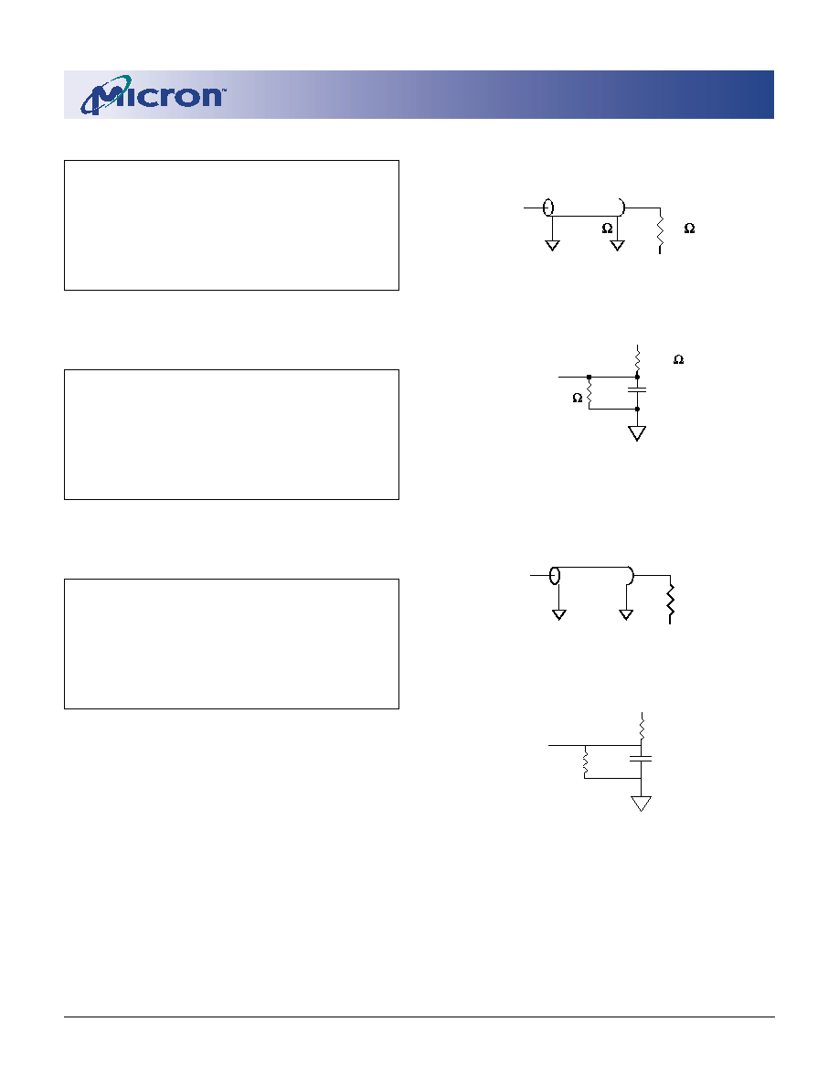
24
18Mb: 1 Meg x 18, 512K x 32/36 Flow-Through SyncBurst SRAM
Micron Technology, Inc., reserves the right to change products or specifications without notice.
MT58L1MY18F_C.p65 ≠ Rev. C, Pub. 9/01
©2001, Micron Technology, Inc.
18Mb: 1 MEG x 18, 512K x 32/36
FLOW-THROUGH SYNCBURST SRAM
ADVANCE
Figure 1
Q
50
V = 1.5V
Z = 50
O
T
Q
351
317
5pF
+3.3V
Figure 2
LOAD DERATING CURVES
Micron 1 Meg x 18, 512K x 32, and 512K x 36 SyncBurst
SRAM timing is dependent upon the capacitive loading
on the outputs.
Consult the factory for copies of I/O current versus
voltage curves.
3.3V V
DD
, 3.3V I/O AC TEST CONDITIONS
Input pulse levels ................... V
IH
= (V
DD
/2.2) + 1.5V
.................... V
IL
= (V
DD
/2.2) - 1.5V
Input rise and fall times ...................................... 1ns
Input timing reference levels ....................... V
DD
/2.2
Output reference levels ............................. V
DD
Q/2.2
Output load .............................. See Figures 1 and 2
Q
50
V = 1.25V
Z = 50
O
T
Figure 3
Q
225
225
5pF
+2.5V
Figure 4
3.3V V
DD
, 2.5V I/O AC TEST CONDITIONS
Input pulse levels ............... V
IH
= (V
DD
/2.64) + 1.25V
................ V
IL
= (V
DD
/2.64) - 1.25V
Input rise and fall times ...................................... 1ns
Input timing reference levels ..................... V
DD
/2.64
Output reference levels ................................ V
DD
Q/2
Output load .............................. See Figures 3 and 4
2.5V V
DD
, 2.5V I/O AC TEST CONDITIONS
Input pulse levels .................... V
IH
= (V
DD
/2) + 1.25V
..................... V
IL
= (V
DD
/2) - 1.25V
Input rise and fall times ...................................... 1ns
Input timing reference levels .......................... V
DD
/2
Output reference levels ................................... V
DD
/2
Output load .............................. See Figures 3 and 4
3.3V I/O Output Load Equivalents
2.5V I/O Output Load Equivalents
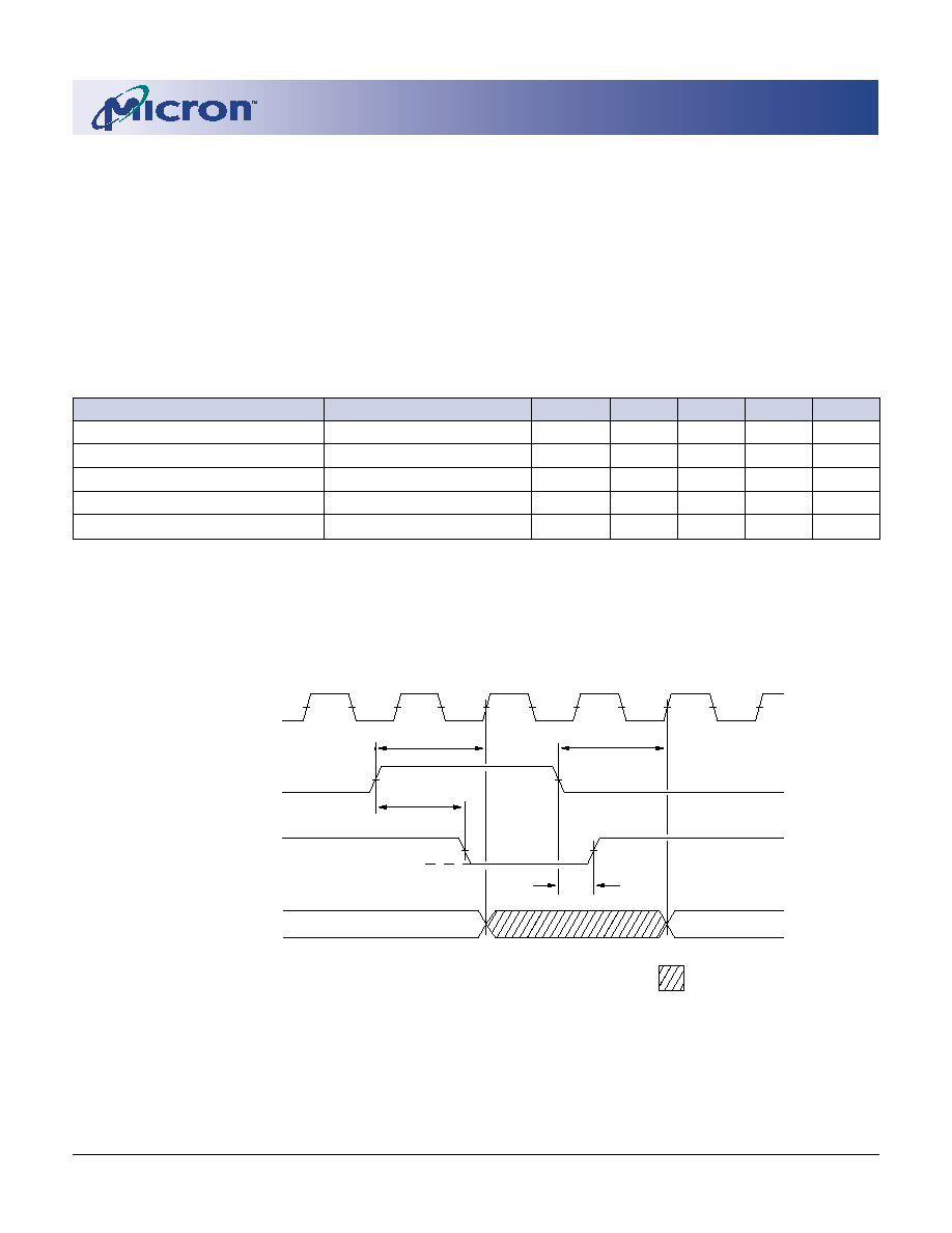
25
18Mb: 1 Meg x 18, 512K x 32/36 Flow-Through SyncBurst SRAM
Micron Technology, Inc., reserves the right to change products or specifications without notice.
MT58L1MY18F_C.p65 ≠ Rev. C, Pub. 9/01
©2001, Micron Technology, Inc.
18Mb: 1 MEG x 18, 512K x 32/36
FLOW-THROUGH SYNCBURST SRAM
ADVANCE
SNOOZE MODE
SNOOZE MODE is a low-current, "power-down" mode
in which the device is deselected and current is reduced to
I
SB
2Z
. The duration of SNOOZE MODE is dictated by the
length of time ZZ is in a HIGH state. After the device enters
SNOOZE MODE, all inputs except ZZ become gated in-
puts and are ignored.
ZZ is an asynchronous, active HIGH input that causes
the device to enter SNOOZE MODE. When ZZ becomes a
logic HIGH, I
SB
2Z
is guaranteed after the setup time
t
ZZ is
met. Any READ or WRITE operation pending when the
device enters SNOOZE MODE is not guaranteed to com-
plete successfully. Therefore, SNOOZE MODE must not
be initiated until valid pending operations are completed.
SNOOZE MODE ELECTRICAL CHARACTERISTICS
DESCRIPTION
CONDITIONS
SYMBOL
MIN
MAX
UNITS
NOTES
Current during SNOOZE MODE
ZZ
V
IH
I
SB
2Z
10
mA
ZZ active to input ignored
t
ZZ
t
KC
ns
1
ZZ inactive to input sampled
t
RZZ
t
KC
ns
1
ZZ active to snooze current
t
ZZI
t
KC
ns
1
ZZ inactive to exit snooze current
t
RZZI
0
ns
1
NOTE: 1. This parameter is sampled.
SNOOZE MODE WAVEFORM
tZZ
I
SUPPLY
CLK
ZZ
I
SB2
ALL INPUTS*
* Except ZZ
DON'T CARE
tZZI
tRZZ
tRZZI
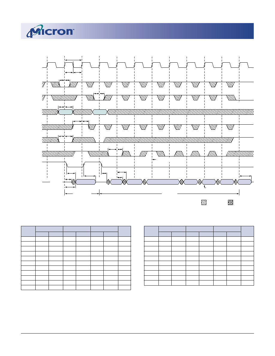
26
18Mb: 1 Meg x 18, 512K x 32/36 Flow-Through SyncBurst SRAM
Micron Technology, Inc., reserves the right to change products or specifications without notice.
MT58L1MY18F_C.p65 ≠ Rev. C, Pub. 9/01
©2001, Micron Technology, Inc.
18Mb: 1 MEG x 18, 512K x 32/36
FLOW-THROUGH SYNCBURST SRAM
ADVANCE
READ TIMING
3
tKC
tKL
CLK
ADSP#
tADSH
tADSS
ADDRESS
tKH
OE#
ADSC#
CE#
(NOTE 2)
tAH
tAS
A1
tCEH
tCES
Q
High-Z
tKQLZ
tKQX
tKQ
ADV#
tOEHZ
tKQ
Single READ
BURST
READ
tOEQ
tOELZ
tKQHZ
Burst wraps around
to its initial state.
tAAH
tAAS
tWH
tWS
tADSH
tADSS
Q(A2)
Q(A2 + 1)
Q(A2 + 2)
Q(A1)
Q(A2)
Q(A2 + 1)
Q(A2 + 2)
Q(A2 + 3)
A2
(NOTE 1)
ADV# suspends burst.
Deselect Cycle
(Note 4)
BWE#, GW#,
BWa#-BWd#
DON'T CARE
UNDEFINED
NOTE: 1. Q(A2) refers to output from address A2. Q(A2 + 1) refers to output from the next internal burst address following A2.
2. CE2# and CE2 have timing identical to CE#. On this diagram, when CE# is LOW, CE2# is LOW and CE2 is HIGH. When
CE# is HIGH, CE2# is HIGH and CE2 is LOW.
3. Timing is shown assuming that the device was not enabled before entering into this sequence.
4. Outputs are disabled
t
KQHZ after deselect.
-7.5
-8.5
-10
SYM
MIN
MAX
MIN
MAX
MIN
MAX
UNITS
t
AS
1.5
1.8
2.0
ns
t
ADSS
1.5
1.8
2.0
ns
t
AAS
1.5
1.8
2.0
ns
t
WS
1.5
1.8
2.0
ns
t
CES
1.5
1.8
2.0
ns
t
AH
0.5
0.5
0.5
ns
t
ADSH
0.5
0.5
0.5
ns
t
AAH
0.5
0.5
0.5
ns
t
WH
0.5
0.5
0.5
ns
t
CEH
0.5
0.5
0.5
ns
READ TIMING PARAMETERS
-7.5
-8.5
-10
SYM
MIN
MAX
MIN
MAX
MIN
MAX
UNITS
t
KC
8.8
10.0
15
ns
f
KF
113
100
66
MHz
t
KH
2.5
3.0
4.0
ns
t
KL
2.5
3.0
4.0
ns
t
KQ
7.5
8.5
10.0
ns
t
KQX
1.5
2.5
2.5
ns
t
KQLZ
1.5
2.5
2.5
ns
t
KQHZ
4.2
5.0
5.0
ns
t
OEQ
4.2
5.0
5.0
ns
t
OELZ
0
0
0
ns
t
OEHZ
4.2
5.0
5.0
ns
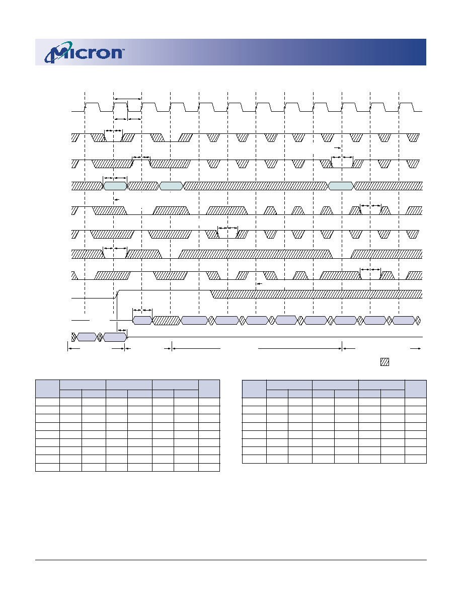
27
18Mb: 1 Meg x 18, 512K x 32/36 Flow-Through SyncBurst SRAM
Micron Technology, Inc., reserves the right to change products or specifications without notice.
MT58L1MY18F_C.p65 ≠ Rev. C, Pub. 9/01
©2001, Micron Technology, Inc.
18Mb: 1 MEG x 18, 512K x 32/36
FLOW-THROUGH SYNCBURST SRAM
ADVANCE
WRITE TIMING
NOTE: 1. D(A2) refers to output from address A2. D(A2 + 1) refers to output from the next internal burst address following A2.
2. CE2# and CE2 have timing identical to CE#. On this diagram, when CE# is LOW, CE2# is LOW and CE2 is HIGH. When
CE# is HIGH, CE2# is HIGH and CE2 is LOW.
3. OE# must be HIGH before the input data setup and held HIGH throughout the data hold time. This prevents input/
output data contention for the time period prior to the byte write enable inputs being sampled.
4. ADV# must be HIGH to permit a WRITE to the loaded address.
5. Full-width WRITE can be initiated by GW# LOW; or GW# HIGH and BWE#, BWa# and BWb# LOW for x18 device; or
GW# HIGH and BWE#, BWa#-BWd# LOW for x32 and x36 devices.
-7.5
-8.5
-10
SYM
MIN
MAX
MIN
MAX
MIN
MAX
UNITS
t
DS
1.5
1.8
2.0
ns
t
CES
1.5
1.8
2.0
ns
t
AH
0.5
0.5
0.5
ns
t
ADSH
0.5
0.5
0.5
ns
t
AAH
0.5
0.5
0.5
ns
t
WH
0.5
0.5
0.5
ns
t
DH
0.5
0.5
0.5
ns
t
CEH
0.5
0.5
0.5
ns
WRITE TIMING PARAMETERS
-7.5
-8.5
-10
SYM
MIN
MAX
MIN
MAX
MIN
MAX
UNITS
t
KC
8.8
10.0
15
ns
f
KF
113
100
66
MHz
t
KH
2.5
3.0
4.0
ns
t
KL
2.5
3.0
4.0
ns
t
OEHZ
4.2
5.0
5.0
ns
t
AS
1.5
1.8
2.0
ns
t
ADSS
1.5
1.8
2.0
ns
t
AAS
1.5
1.8
2.0
ns
t
WS
1.5
1.8
2.0
ns
tKC
tKL
CLK
ADSP#
tADSH
tADSS
ADDRESS
tKH
OE#
ADSC#
CE#
(NOTE 2)
tAH
tAS
A1
tCEH
tCES
Q
High-Z
ADV#
BURST READ
BURST WRITE
D(A2)
D(A2 + 1)
D(A2 + 1)
D(A1)
D(A3)
D(A3 + 1)
D(A3 + 2)
D(A2 + 3)
A2
A3
D
Extended BURST WRITE
D(A2 + 2)
Single WRITE
tADSH
tADSS
tADSH
tADSS
tOEHZ
tAAH
tAAS
tWH
tWS
tDH
tDS
(NOTE 3)
(NOTE 1)
(NOTE 4)
GW#
tWH
tWS
(NOTE 5)
BYTE WRITE signals are
ignored when ADSP# is LOW.
ADSC# extends burst.
ADV# suspends burst.
BWE#,
BWa#-BWd#
DON'T CARE
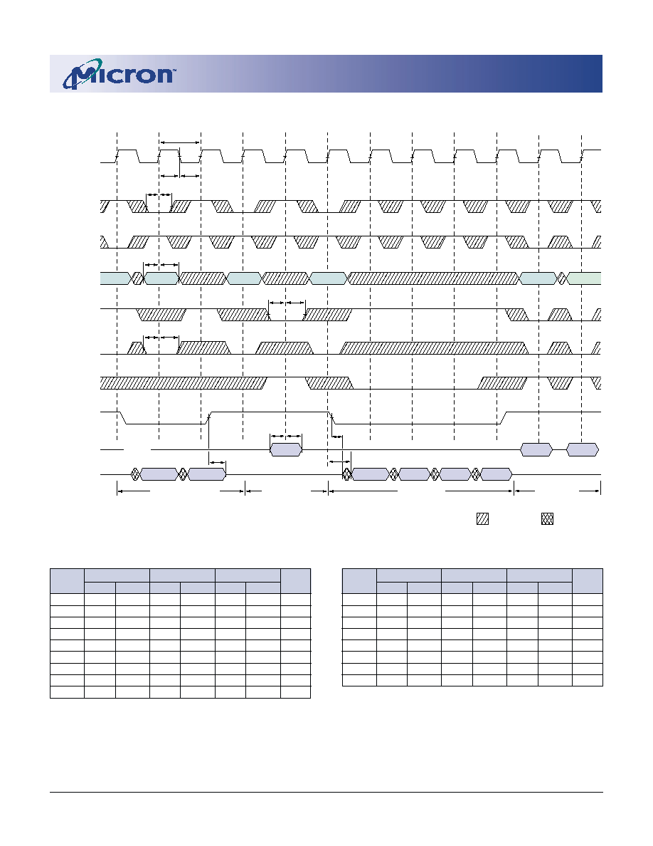
28
18Mb: 1 Meg x 18, 512K x 32/36 Flow-Through SyncBurst SRAM
Micron Technology, Inc., reserves the right to change products or specifications without notice.
MT58L1MY18F_C.p65 ≠ Rev. C, Pub. 9/01
©2001, Micron Technology, Inc.
18Mb: 1 MEG x 18, 512K x 32/36
FLOW-THROUGH SYNCBURST SRAM
ADVANCE
t
WS
1.5
1.8
2.0
ns
t
DS
1.5
1.8
2.0
ns
t
CES
1.5
1.8
2.0
ns
t
AH
0.5
0.5
0.5
ns
t
ADSH
0.5
0.5
0.5
ns
t
WH
0.5
0.5
0.5
ns
t
DH
0.5
0.5
0.5
ns
t
CEH
0.5
0.5
0.5
ns
READ/WRITE TIMING
3
NOTE: 1. Q(A4) refers to output from address A4. Q(A4 + 1) refers to output from the next internal burst address following A4.
2. CE2# and CE2 have timing identical to CE#. On this diagram, when CE# is LOW, CE2# is LOW and CE2 is HIGH. When
CE# is HIGH, CE2# is HIGH and CE2 is LOW.
3. The data bus (Q) remains in High-Z following a WRITE cycle unless an ADSP#, ADSC#, or ADV# cycle is performed.
4. GW# is HIGH.
5. Back-to-back READs may be controlled by either ADSP# or ADSC#.
READ/WRITE TIMING PARAMETERS
-7.5
-8.5
-10
SYM
MIN
MAX
MIN
MAX
MIN
MAX
UNITS
t
KC
8.8
10.0
15
ns
f
KF
113
100
66
MHz
t
KH
2.5
3.0
4.0
ns
t
KL
2.5
3.0
4.0
ns
t
KQ
7.5
8.5
10.0
ns
t
OELZ
0
0
0
ns
t
OEHZ
4.2
5.0
5.0
ns
t
AS
1.5
1.8
2.0
ns
t
ADSS
1.5
1.8
2.0
ns
-7.5
-8.5
-10
SYM
MIN
MAX
MIN
MAX
MIN
MAX
UNITS
tKC
tKL
CLK
ADSP#
tADSH
tADSS
ADDRESS
tKH
OE#
ADSC#
CE#
(NOTE 2)
tAH
tAS
A2
tCEH
tCES
Q
ADV#
Single WRITE
D(A3)
A3
A4
D
BURST READ
Back-to-Back READs
(NOTE 5)
High-Z
Q(A2)
Q(A4)
Q(A4+1)
Q(A4+2)
Q(A4+3)
tWH
tWS
tOEHZ
tDH
tDS
tKQ
tOELZ
(NOTE 1)
A1
A5
A6
D(A5)
D(A6)
Q(A1)
Back-to-Back
WRITEs
BWE#,
BWa#-BWd#
(NOTE 4)
DON'T CARE
UNDEFINED
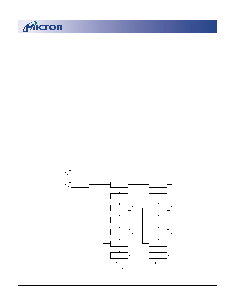
29
18Mb: 1 Meg x 18, 512K x 32/36 Flow-Through SyncBurst SRAM
Micron Technology, Inc., reserves the right to change products or specifications without notice.
MT58L1MY18F_C.p65 ≠ Rev. C, Pub. 9/01
©2001, Micron Technology, Inc.
18Mb: 1 MEG x 18, 512K x 32/36
FLOW-THROUGH SYNCBURST SRAM
ADVANCE
IEEE 1149.1 SERIAL BOUNDARY SCAN
(JTAG)
The SRAM incorporates a serial boundary scan test
access port (TAP). This port operates in accordance with
IEEE Standard 1149.1-1990 but does not have the set of
functions required for full 1149.1 compliance. These func-
tions from the IEEE specification are excluded because
their inclusion places an added delay in the critical speed
path of the SRAM. Note that the TAP controller functions
in a manner that does not conflict with the operation of
other devices using 1149.1 fully compliant TAPs. The TAP
operates using JEDEC-standard 2.5V I/O logic levels.
The SRAM contains a TAP controller, instruction
register, boundary scan register, bypass register, and ID
register.
DISABLING THE JTAG FEATURE
These pins can be left floating (unconnected), if the
JTAG function is not to be implemented. Upon power-up,
the device will come up in a reset state which will not
interfere with the operation of the device.
TEST ACCESS PORT (TAP)
TEST CLOCK (TCK)
The test clock is used only with the TAP controller. All
inputs are captured on the rising edge of TCK. All outputs
are driven from the falling edge of TCK.
TEST MODE SELECT (TMS)
The TMS input is used to give commands to the TAP
controller and is sampled on the rising edge of TCK. It is
allowable to leave this pin unconnected if the TAP is not
used. The pin is pulled up internally, resulting in a logic
HIGH level.
TEST DATA-IN (TDI)
The TDI pin is used to serially input information into
the registers and can be connected to the input of any of
the registers. The register between TDI and TDO is chosen
by the instruction that is loaded into the TAP instruction
register. For information on loading the instruction regis-
ter, see Figure 5. TDI is internally pulled up and can be
unconnected if the TAP is unused in an application. TDI is
connected to the most significant bit (MSB) of any regis-
ter. (See Figure 6.)
Figure 5
TAP Controller State Diagram
NOTE: The 0/1 next to each state represents the value of TMS at the rising edge of TCK.
TEST-LOGIC
RESET
RUN-TEST/
IDLE
SELECT
DR-SCAN
SELECT
IR-SCAN
CAPTURE-DR
SHIFT-DR
CAPTURE-IR
SHIFT-IR
EXIT1-DR
PAUSE-DR
EXIT1-IR
PAUSE-IR
EXIT2-DR
UPDATE-DR
EXIT2-IR
UPDATE-IR
1
1
1
0
1
1
0
0
1
1
1
0
0
0
0
0
0
0
0
0
1
0
1
1
0
1
0
1
1
1
1
0
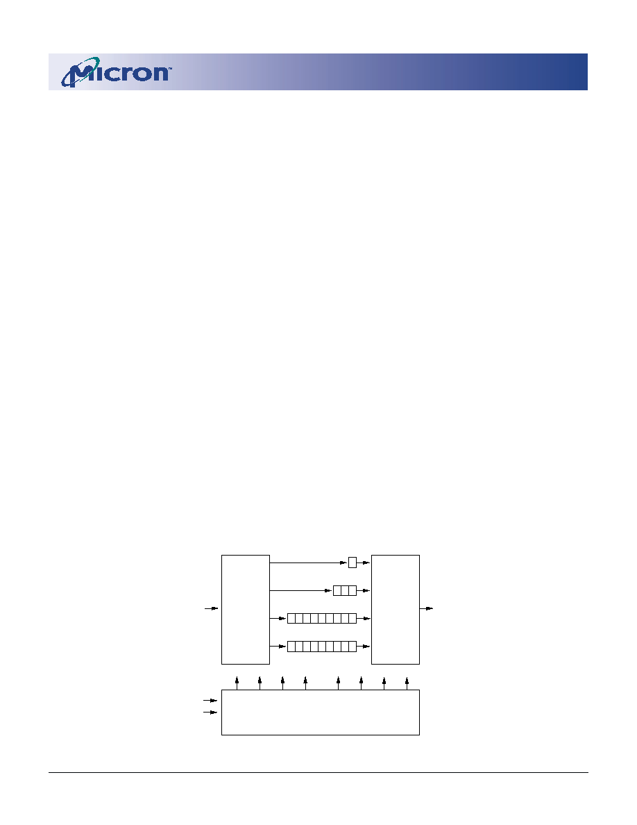
30
18Mb: 1 Meg x 18, 512K x 32/36 Flow-Through SyncBurst SRAM
Micron Technology, Inc., reserves the right to change products or specifications without notice.
MT58L1MY18F_C.p65 ≠ Rev. C, Pub. 9/01
©2001, Micron Technology, Inc.
18Mb: 1 MEG x 18, 512K x 32/36
FLOW-THROUGH SYNCBURST SRAM
ADVANCE
TEST DATA-OUT (TDO)
The TDO output pin is used to serially clock data-out
from the registers. The output is active depending upon
the current state of the TAP state machine. (See Figure 5.)
The output changes on the falling edge of TCK. TDO is
connected to the least significant bit (LSB) of any register.
(See Figure 6.)
PERFORMING A TAP RESET
A RESET is performed by forcing TMS HIGH (V
DD
) for
five rising edges of TCK. This RESET does not affect the
operation of the SRAM and may be performed while the
SRAM is operating.
At power-up, the TAP is reset internally to ensure that
TDO comes up in a High-Z state.
TAP REGISTERS
Registers are connected between the TDI and TDO
pins and allow data to be scanned into and out of the
SRAM test circuitry. Only one register can be selected at a
time through the instruction register. Data is serially
loaded into the TDI pin on the rising edge of TCK. Data is
output on the TDO pin on the falling edge of TCK.
INSTRUCTION REGISTER
Three-bit instructions can be serially loaded into the
instruction register. This register is loaded when it is placed
between the TDI and TDO pins as shown in Figure 5. Upon
power-up, the instruction register is loaded with the
IDCODE instruction. It is also loaded with the IDCODE
instruction if the controller is placed in a reset state as
described in the previous section.
When the TAP controller is in the Capture-IR state, the
two least significant bits are loaded with a binary "01"
pattern to allow for fault isolation of the board-level serial
test data path.
BYPASS REGISTER
To save time when serially shifting data through regis-
ters, it is sometimes advantageous to skip certain chips.
The bypass register is a single-bit register that can be
placed between the TDI and TDO pins. This allows data to
be shifted through the SRAM with minimal delay. The
bypass register is set LOW (V
SS
) when the BYPASS instruc-
tion is executed.
BOUNDARY SCAN REGISTER
The boundary scan register is connected to all the
input and bidirectional pins on the SRAM. The x36 con-
figuration has a 71-bit-long register, 67-bit-long regis-
ter, and the x18 configuration has a 52-bit-long regis-
ter.
The boundary scan register is loaded with the contents
of the RAM I/O ring when the TAP controller is in the
Capture-DR state and is then placed between the TDI and
TDO pins when the controller is moved to the Shift-DR
state. The EXTEST, SAMPLE/PRELOAD and SAMPLE Z
instructions can be used to capture the contents of the
I/O ring.
The Boundary Scan Order tables show the order in
which the bits are connected. Each bit corresponds to one
of the bumps on the SRAM package. The MSB of the
register is connected to TDI, and the LSB is connected to
TDO.
Bypass Register
0
Instruction Register
0
1
2
Identification Register
0
1
2
29
30
31
.
.
.
Boundary Scan Register*
0
1
2
.
.
x
.
.
.
Selection
Circuitry
Selection
Circuitry
TCK
TMS
TAP CONTROLLER
TDI
TDO
*x = 52 for the x18 configuration, x = 67 for the x32 configuration,
x = 71 for the x36 configuration.
Figure 6
TAP Controller Block Diagram

31
18Mb: 1 Meg x 18, 512K x 32/36 Flow-Through SyncBurst SRAM
Micron Technology, Inc., reserves the right to change products or specifications without notice.
MT58L1MY18F_C.p65 ≠ Rev. C, Pub. 9/01
©2001, Micron Technology, Inc.
18Mb: 1 MEG x 18, 512K x 32/36
FLOW-THROUGH SYNCBURST SRAM
ADVANCE
IDENTIFICATION (ID) REGISTER
The ID register is loaded with a vendor-specific, 32-bit
code during the Capture-DR state when the IDCODE com-
mand is loaded in the instruction register. The IDCODE is
hardwired into the SRAM and can be shifted out when the
TAP controller is in the Shift-DR state. The ID register has
a vendor code and other information described in the
Identification Register Definitions table.
TAP INSTRUCTION SET
OVERVIEW
Eight different instructions are possible with the three-
bit instruction register. All combinations are listed in the
Instruction Codes table. Three of these instructions are
listed as RESERVED and should not be used. The other
five instructions are described in detail below.
The TAP controller used in this SRAM is not fully com-
pliant to the 1149.1 convention because some of the man-
datory 1149.1 instructions are not fully implemented. The
TAP controller cannot be used to load address, data or
control signals into the SRAM and cannot preload the I/O
buffers. The SRAM does not implement the 1149.1 com-
mands EXTEST or INTEST or the PRELOAD portion of
SAMPLE/PRELOAD; rather, it performs a capture of the
I/O ring when these instructions are executed.
Instructions are loaded into the TAP controller during
the Shift-IR state when the instruction register is placed
between TDI and TDO. During this state, instructions are
shifted through the instruction register through the TDI
and TDO pins. To execute the instruction once it is shifted
in, the TAP controller needs to be moved into the Update-
IR state.
EXTEST
EXTEST is a mandatory 1149.1 instruction which is to
be executed whenever the instruction register is loaded
with all 0s. EXTEST is not implemented in this SRAM TAP
controller, and therefore this device is not compliant to
1149.1.
The TAP controller does recognize an all-0 instruction.
When an EXTEST instruction is loaded into the instruc-
tion register, the SRAM responds as if a SAMPLE/PRELOAD
instruction has been loaded. There is one difference be-
tween the two instructions. Unlike the SAMPLE/PRELOAD
instruction, EXTEST places the SRAM outputs in a High-Z
state.
IDCODE
The IDCODE instruction causes a vendor-specific, 32-
bit code to be loaded into the instruction register. It also
places the instruction register between the TDI and TDO
pins and allows the IDCODE to be shifted out of the device
when the TAP controller enters the Shift-DR state. The
IDCODE instruction is loaded into the instruction register
upon power-up or whenever the TAP controller is given a
test logic reset state.
SAMPLE Z
The SAMPLE Z instruction causes the boundary scan
register to be connected between the TDI and TDO pins
when the TAP controller is in a Shift-DR state. It also
places all SRAM outputs into a High-Z state.
SAMPLE/PRELOAD
SAMPLE/PRELOAD is a 1149.1 mandatory instruction.
The PRELOAD portion of this instruction is not imple-
mented, so the device TAP controller is not fully 1149.1-
compliant.
When the SAMPLE/PRELOAD instruction is loaded
into the instruction register and the TAP controller is in
the Capture-DR state, a snapshot of data on the inputs and
bidirectional pins is captured in the boundary scan regis-
ter.
The user must be aware that the TAP controller clock
can only operate at a frequency up to 10 MHz, while the
SRAM clock operates more than an order of magnitude
faster. Because there is a large difference in the clock
frequencies, it is possible that during the Capture-DR
state, an input or output will undergo a transition. The
TAP may then try to capture a signal while in transition
(metastable state). This will not harm the device, but there
is no guarantee as to the value that will be captured.
Repeatable results may not be possible.
To guarantee that the boundary scan register will cap-
ture the correct value of a signal, the SRAM signal must be
stabilized long enough to meet the TAP controller's cap-
ture setup plus hold time (
t
CS plus
t
CH). The SRAM clock
input might not be captured correctly if there is no way in
a design to stop (or slow) the clock during a SAMPLE/
PRELOAD instruction. If this is an issue, it is still possible
to capture all other signals and simply ignore the value of
the CK and CK# captured in the boundary scan register.
Once the data is captured, it is possible to shift out the
data by putting the TAP into the Shift-DR state. This places
the boundary scan register between the TDI and TDO
pins.
Note that since the PRELOAD part of the command is
not implemented, putting the TAP to the Update-DR state
while performing a SAMPLE/PRELOAD instruction will
have the same effect as the Pause-DR command.
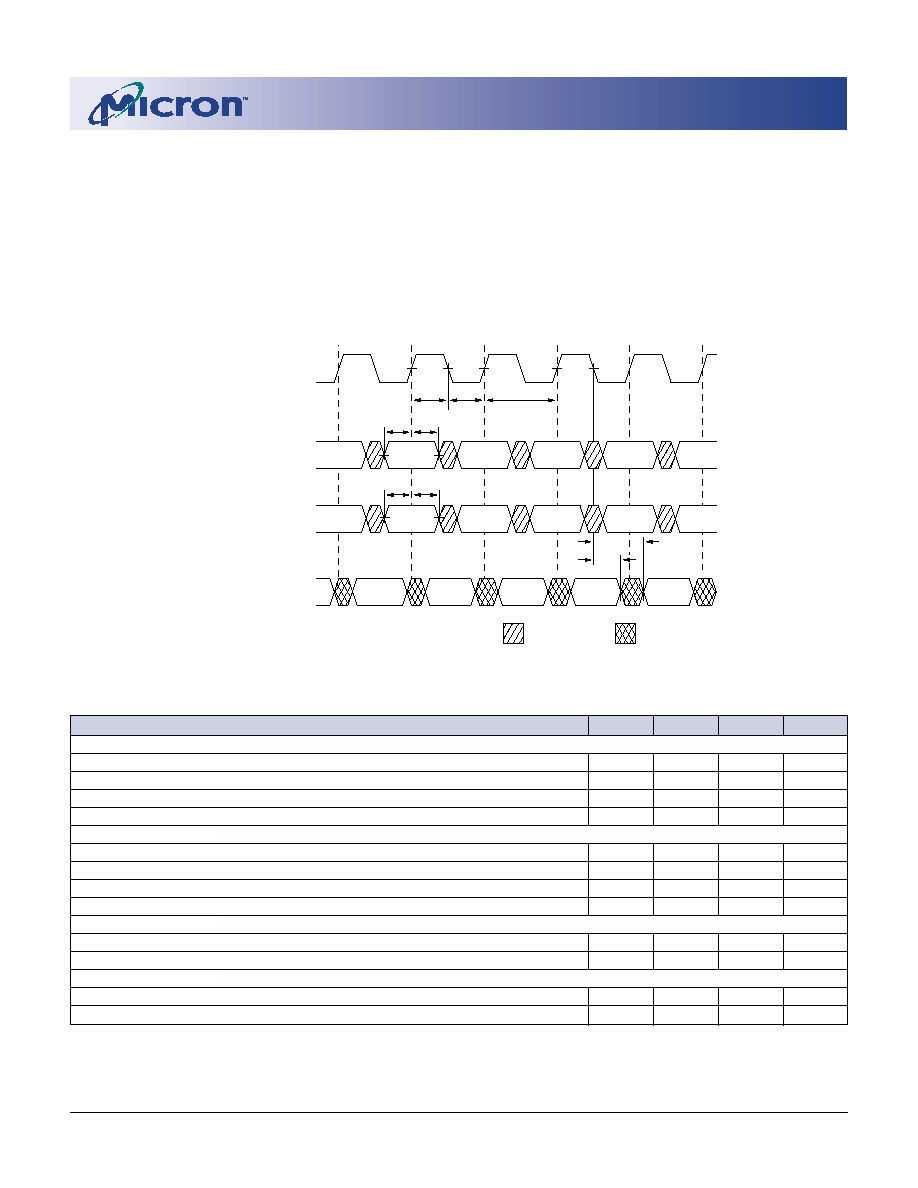
32
18Mb: 1 Meg x 18, 512K x 32/36 Flow-Through SyncBurst SRAM
Micron Technology, Inc., reserves the right to change products or specifications without notice.
MT58L1MY18F_C.p65 ≠ Rev. C, Pub. 9/01
©2001, Micron Technology, Inc.
18Mb: 1 MEG x 18, 512K x 32/36
FLOW-THROUGH SYNCBURST SRAM
ADVANCE
BYPASS
When the BYPASS instruction is loaded in the instruc-
tion register and the TAP is placed in a Shift-DR state, the
bypass register is placed between TDI and TDO. The ad-
vantage of the BYPASS instruction is that it shortens the
boundary scan path when multiple devices are connected
together on a board.
RESERVED
These instruction are not implemented but are re-
served for future use. Do not use these instructions.
t
TLTH
Test Clock
(TCK)
1
2
3
4
5
6
Test Mode Select
(TMS)
tTHTL
Test Data-Out
(TDO)
tTHTH
Test Data-In
(TDI)
tTHMX
tMVTH
tTHDX
tDVTH
tTLOX
tTLOV
DON'T CARE
UNDEFINED
TAP TIMING
TAP AC ELECTRICAL CHARACTERISTICS
(Notes 1, 2) (+20∫C
T
J
+100∫C; +2.4V V
DD
+2.6V)
DESCRIPTION
SYMBOL
MIN
MAX
UNITS
Clock
Clock cycle time
t
THTH
100
ns
Clock frequency
f
TF
10
MHz
Clock HIGH time
t
THTL
40
ns
Clock LOW time
t
TLTH
40
ns
Output Times
TCK LOW to TDO unknown
t
TLOX
0
ns
TCK LOW to TDO valid
t
TLOV
20
ns
TDI valid to TCK HIGH
t
DVTH
10
ns
TCK HIGH to TDI invalid
t
THDX
10
ns
Setup Times
TMS setup
t
MVTH
10
ns
Capture setup
t
CS
10
ns
Hold Times
TMS hold
t
THMX
10
ns
Capture hold
t
CH
10
ns
NOTE: 1.
t
CS and
t
CH refer to the setup and hold time requirements of latching data from the boundary scan register.
2. Test conditions are specified using the load in Figure 7.
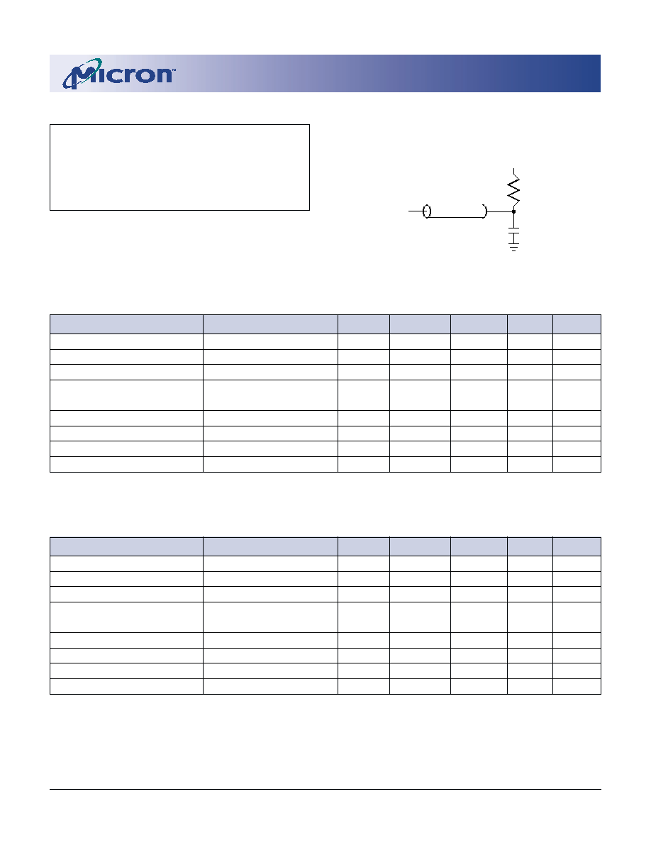
33
18Mb: 1 Meg x 18, 512K x 32/36 Flow-Through SyncBurst SRAM
Micron Technology, Inc., reserves the right to change products or specifications without notice.
MT58L1MY18F_C.p65 ≠ Rev. C, Pub. 9/01
©2001, Micron Technology, Inc.
18Mb: 1 MEG x 18, 512K x 32/36
FLOW-THROUGH SYNCBURST SRAM
ADVANCE
TAP AC TEST CONDITIONS
Input pulse levels ....................................... V
SS
to 2.5V
Input rise and fall times ......................................... 1ns
Input timing reference levels ............................. 1.25V
Output reference levels ..................................... 1.25V
Test load termination supply voltage ............... 1.25V
TDO
1.25V
20pF
Z = 50
O
50
Figure 7
TAP AC Output Load Equivalent
3.3V V
DD
, TAP DC ELECTRICAL CHARACTERISTICS AND OPERATING CONDITIONS
(+20∫C
T
J
+110∫C; +2.4V V
DD
+2.6V unless otherwise noted)
DESCRIPTION
CONDITIONS
SYMBOL
MIN
MAX
UNITS
NOTES
Input High (Logic 1) Voltage
V
IH
2.0
V
DD
+ 0.3
V
1, 2
Input Low (Logic 0) Voltage
V
IL
-0.3
0.8
V
1, 2
Input Leakage Current
0V
V
IN
V
DD
IL
I
-5.0
5.0
µA
Output Leakage Current
Output(s) disabled,
IL
O
-5.0
5.0
µA
0V
V
IN
V
DD
Q (DQx)
Output Low Voltage
I
OLC
= 100µA
V
OL
1
0.7
V
1
Output Low Voltage
I
OLT
= 2mA
V
OL
2
0.8
V
1
Output High Voltage
I
OHC
= -100µA
V
OH
1
2.9
V
1
Output High Voltage
I
OHT
= -2mA
V
OH
2
2.0
V
1
NOTE: 1. All voltages referenced to V
SS
(GND).
2. Overshoot:
V
IH
(AC)
V
DD
+ 1.5V for t
t
KHKH/2
Undershoot:
V
IL
(AC)
-0.5V for t
t
KHKH/2
Power-up:
V
IH
+2.6V and V
DD
2.4V and V
DD
Q
1.4V for t 200ms
During normal operation, V
DD
Q must not exceed V
DD
. Control input signals (such as LD#, R/W#, etc.) may not have
pulse widths less than
t
KHKL (MIN) or operate at frequencies exceeding
f
KF (MAX).
2.5V V
DD
, TAP DC ELECTRICAL CHARACTERISTICS AND OPERATING CONDITIONS
(+20∫C
T
J
+110∫C; +2.4V V
DD
+2.6V unless otherwise noted)
DESCRIPTION
CONDITIONS
SYMBOL
MIN
MAX
UNITS
NOTES
Input High (Logic 1) Voltage
V
IH
1.7
V
DD
+ 0.3
V
1, 2
Input Low (Logic 0) Voltage
V
IL
-0.3
0.7
V
1, 2
Input Leakage Current
0V
V
IN
V
DD
IL
I
-5.0
5.0
µA
Output Leakage Current
Output(s) disabled,
IL
O
-5.0
5.0
µA
0V
V
IN
V
DD
Q (DQx)
Output Low Voltage
I
OLC
= 100µA
V
OL
1
0.2
V
1
Output Low Voltage
I
OLT
= 2mA
V
OL
2
0.7
V
1
Output High Voltage
I
OHC
= -100µA
V
OH
1
2.1
V
1
Output High Voltage
I
OHT
= -2mA
V
OH
2
1.7
V
1
34
18Mb: 1 Meg x 18, 512K x 32/36 Flow-Through SyncBurst SRAM
Micron Technology, Inc., reserves the right to change products or specifications without notice.
MT58L1MY18F_C.p65 ≠ Rev. C, Pub. 9/01
©2001, Micron Technology, Inc.
18Mb: 1 MEG x 18, 512K x 32/36
FLOW-THROUGH SYNCBURST SRAM
ADVANCE
IDENTIFICATION REGISTER DEFINITIONS
INSTRUCTION FIELD
512K x 18
DESCRIPTION
REVISION NUMBER
xxxx
Reserved for version number.
(31:28)
DEVICE DEPTH
00111
Defines depth of 512K or 1Mb words.
(27:23)
DEVICE WIDTH
00011
Defines width of x18, x32, or x36 bits.
(22:18)
MICRON DEVICE ID
xxxxxx
Reserved for future use.
(17:12)
MICRON JEDEC ID
00000101100
Allows unique identification of SRAM vendor.
CODE (11:1)
ID Register Presence
1
Indicates the presence of an ID register.
Indicator (0)
INSTRUCTION CODES
INSTRUCTION
CODE
DESCRIPTION
EXTEST
000
Captures I/O ring contents. Places the boundary scan register between TDI and TDO.
Forces all SRAM outputs to High-Z state. This instruction is not 1149.1-compliant.
IDCODE
001
Loads the ID register with the vendor ID code and places the register between TDI
and TDO. This operation does not affect SRAM operations.
SAMPLE Z
010
Captures I/O ring contents. Places the boundary scan register between TDI and TDO.
Forces all SRAM output drivers to a High-Z state.
RESERVED
011
Do Not Use: This instruction is reserved for future use.
SAMPLE/PRELOAD
100
Captures I/O ring contents. Places the boundary scan register between TDI and TDO.
Does not affect SRAM operation. This instruction does not implement 1149.1
preload function and is therefore not 1149.1-compliant.
RESERVED
101
Do Not Use: This instruction is reserved for future use.
RESERVED
110
Do Not Use: This instruction is reserved for future use.
BYPASS
111
Places the bypass register between TDI and TDO. This operation does not affect
SRAM operations.
SCAN REGISTER SIZES
REGISTER NAME
BIT SIZE
Instruction
3
Bypass
1
ID
32
Boundary Scan
x18: 52
x32: 67
x36: 71
35
18Mb: 1 Meg x 18, 512K x 32/36 Flow-Through SyncBurst SRAM
Micron Technology, Inc., reserves the right to change products or specifications without notice.
MT58L1MY18F_C.p65 ≠ Rev. C, Pub. 9/01
©2001, Micron Technology, Inc.
18Mb: 1 MEG x 18, 512K x 32/36
FLOW-THROUGH SYNCBURST SRAM
ADVANCE
165-PIN FBGA BOUNDARY SCAN ORDER (x18)
28
GWE#
7B
29
CLK
6B
30
CE2#
6A
31
BWa#
5B
32
BWb#
4A
33
CE2
3B
34
CE#
3A
35
SA
2A
36
SA
2B
37
DQb
2D
38
DQb
2E
39
DQb
2F
40
DQb
2G
41
V
SS
1H
42
DQb
1J
43
DQb
1K
44
DQb
1L
45
DQb
1M
46
DQPb
1N
47
MODE (LBO#)
1R
48
SA
3P
49
SA
3R
50
SA
4P
51
SA
4R
52
SA1
6P
53
SA0
6R
FBGA BIT#
SIGNAL NAME
PIN ID
FBGA BIT#
SIGNAL NAME
PIN ID
1
SA
6N
2
SA
11P
3
SA
8P
4
SA
9R
5
SA
9P
6
SA
10R
7
SA
10P
8
SA
11R
9
SA
8R
10
DQa
10M
11
DQa
10L
12
DQa
10K
13
DQa
10J
14
ZZ
11H
15
DQa
11G
16
DQa
11F
17
DQa
11E
18
DQa
11D
19
DQPa
11C
20
SA
11A
21
SA
10B
22
SA
10A
23
ADV#
9A
24
ADSP#
9B
25
ADSC#
8A
26
OE# (G#)
8B
27
BWE#
7A

36
18Mb: 1 Meg x 18, 512K x 32/36 Flow-Through SyncBurst SRAM
Micron Technology, Inc., reserves the right to change products or specifications without notice.
MT58L1MY18F_C.p65 ≠ Rev. C, Pub. 9/01
©2001, Micron Technology, Inc.
18Mb: 1 MEG x 18, 512K x 32/36
FLOW-THROUGH SYNCBURST SRAM
ADVANCE
165-PIN FBGA BOUNDARY SCAN ORDER (x32)
35
CLK
6B
36
CE2#
6A
37
BWa#
5B
38
BWb#
5A
39
BWc#
4A
40
BWd#
4B
41
CE2
3B
42
CE#
3A
43
SA
2A
44
SA
2B
45
DQc
1D
46
DQc
1E
47
DQc
1F
48
DQc
1G
49
DQc
2D
50
DQc
2E
51
DQc
2F
52
DQc
2G
53
V
SS
1H
54
DQd
1J
55
DQd
1K
56
DQd
1L
57
DQd
1M
58
DQd
2J
59
DQd
2K
60
DQd
2L
61
DQd
2M
62
MODE (LBO#)
1R
63
SA
3P
64
SA
3R
65
SA
4P
66
SA
4R
67
SA1
6P
68
SA0
6R
FBGA BIT#
SIGNAL NAME
PIN ID
FBGA BIT#
SIGNAL NAME
PIN ID
1
SA
6N
2
SA
11P
3
SA
8P
4
SA
9R
5
SA
9P
6
SA
10R
7
SA
10P
8
SA
11R
9
SA
8R
10
DQa
11M
11
DQa
11L
12
DQa
11K
13
DQa
11J
14
DQa
10M
15
DQa
10L
16
DQa
10K
17
DQa
10J
18
ZZ
11H
19
DQb
11G
20
DQb
11F
21
DQb
11E
22
DQb
11D
23
DQb
10G
24
DQb
10F
25
DQb
10E
26
DQb
10D
27
SA
10B
28
SA
10A
29
ADV#
9A
30
ADSP#
9B
31
ADSC#
8A
32
OE# (G#)
8B
33
BWE#
7A
34
GW#
7B

37
18Mb: 1 Meg x 18, 512K x 32/36 Flow-Through SyncBurst SRAM
Micron Technology, Inc., reserves the right to change products or specifications without notice.
MT58L1MY18F_C.p65 ≠ Rev. C, Pub. 9/01
©2001, Micron Technology, Inc.
18Mb: 1 MEG x 18, 512K x 32/36
FLOW-THROUGH SYNCBURST SRAM
ADVANCE
165-PIN FBGA BOUNDARY SCAN ORDER (x36)
37
CLK
6B
38
CE2#
6A
39
BWa#
5B
40
BWb#
5A
41
BWc#
4A
42
BWd#
4B
43
CE2
3B
44
CE#
3A
45
SA
2A
46
SA
2B
47
NF/
DQPc
1C
48
DQc
1D
49
DQc
1E
50
DQc
1F
51
DQc
1G
52
DQc
2D
53
DQc
2E
54
DQc
2F
55
DQc
2G
56
V
SS
1H
57
DQd
1J
58
DQd
1K
59
DQd
1L
60
DQd
1M
61
DQd
2J
62
DQd
2K
63
DQd
2L
64
DQd
2M
65
NF/
DQPd
1N
66
MODE (LBO#)
1R
67
SA
3P
68
SA
3R
69
SA
4P
70
SA
4R
71
SA1
6P
72
SA0
6R
FBGA BIT#
SIGNAL NAME
PIN ID
FBGA BIT#
SIGNAL NAME
PIN ID
1
SA
6N
2
SA
11P
3
SA
8P
4
SA
9R
5
SA
9P
6
SA
10R
7
SA
10P
8
SA
11R
9
SA
8R
10
NF/
DQPa
11N
11
DQa
11M
12
DQa
11L
13
DQa
11K
14
DQa
11J
15
DQa
10M
16
DQa
10L
17
DQa
10K
18
DQa
10J
19
ZZ
11H
20
DQb
11G
21
DQb
11F
22
DQb
11E
23
DQb
11D
24
DQb
10G
25
DQb
10F
26
DQb
10E
27
DQb
10D
28
NF/
DQPb
11C
29
SA
10B
30
SA
10A
31
ADV#
9A
32
ADSP#
9B
33
ADSC#
8A
34
OE# (G#)
8B
35
BWE#
7A
36
GW#
7B
38
18Mb: 1 Meg x 18, 512K x 32/36 Flow-Through SyncBurst SRAM
Micron Technology, Inc., reserves the right to change products or specifications without notice.
MT58L1MY18F_C.p65 ≠ Rev. C, Pub. 9/01
©2001, Micron Technology, Inc.
18Mb: 1 MEG x 18, 512K x 32/36
FLOW-THROUGH SYNCBURST SRAM
ADVANCE
119-PIN PBGA BOUNDARY SCAN ORDER (x18)
27
CLK
4K
28
SA
6B
29
BWa#
5L
30
BWb#
3G
31
SA
2B
32
CE#
4E
33
SA
3A
34
SA
2A
35
DQb
1D
36
DQb
2E
37
DQb
2G
38
DQb
1H
39
V
SS
5R
40
DQb
2K
41
DQPb
1L
42
DQb
2M
43
DQb
1N
44
DQPb
2P
45
MODE (LBO#)
3R
46
SA
2C
47
SA
3C
48
SA
2R
49
SA
3T
50
SA1
4N
51
SA0
4P
BGA BIT#
SIGNAL NAME
PIN ID
BGA BIT#
SIGNAL NAME
PIN ID
1
SA
2T
2
SA
6R
3
SA
5T
4
SA
3B
5
SA
5B
6
SA
5C
7
SA
6C
8
DQa
7P
9
DQa
6N
10
DQa
6L
11
DQa
7K
12
ZZ
7T
13
DQa
6H
14
DQa
7G
15
DQa
6F
16
DQa
7E
17
DQPa
6D
18
SA
6T
19
SA
6A
20
SA
5A
21
ADV#
4G
22
ADSP
4A
23
ADSC#
4B
24
OE# (G#)
4F
25
BWE#
4M
26
GW#
4H

39
18Mb: 1 Meg x 18, 512K x 32/36 Flow-Through SyncBurst SRAM
Micron Technology, Inc., reserves the right to change products or specifications without notice.
MT58L1MY18F_C.p65 ≠ Rev. C, Pub. 9/01
©2001, Micron Technology, Inc.
18Mb: 1 MEG x 18, 512K x 32/36
FLOW-THROUGH SYNCBURST SRAM
ADVANCE
119-PIN PBGA BOUNDARY SCAN ORDER (x32)
34
SA
6B
35
BWa#
5L
36
BWb#
5G
37
BWc#
3G
38
BWd#
3L
39
SA
2B
40
CE#
4E
41
SA
3A
42
SA
2A
43
DQc
1E
44
DQc
2F
45
DQc
1G
46
DQc
2H
47
DQc
1D
48
DQc
2E
49
DQc
2G
50
DQc
1H
51
V
SS
5R
52
DQd
2K
53
DQd
1L
54
DQd
2M
55
DQd
1N
56
DQd
1P
57
DQd
1K
58
DQd
2L
59
DQd
2N
60
MODE (LBO#)
3R
61
SA
2C
62
SA
3C
63
SA
2R
64
SA
3T
65
SA1
4N
66
SA0
4P
BGA BIT#
SIGNAL NAME
PIN ID
BGA BIT#
SIGNAL NAME
PIN ID
1
SA
4T
2
SA
6R
3
SA
5T
4
SA
3B
5
SA
5B
6
SA
5C
7
SA
6C
8
DQa
7N
9
DQa
6M
10
DQa
7L
11
DQa
6K
12
DQa
7P
13
DQa
6N
14
DQa
6L
15
DQa
7K
16
ZZ
7T
17
DQb
6H
18
DQb
7G
19
DQb
6F
20
DQb
7E
21
DQb
6E
22
DQb
7H
23
DQb
7D
24
DQb
6G
25
SA
6A
26
SA
5A
27
ADV#
4G
28
ADSP#
4A
29
ADSC#
4B
30
OE# (G#)
4F
31
BWE#
4M
32
GW#
4H
33
CLK
4K
40
18Mb: 1 Meg x 18, 512K x 32/36 Flow-Through SyncBurst SRAM
Micron Technology, Inc., reserves the right to change products or specifications without notice.
MT58L1MY18F_C.p65 ≠ Rev. C, Pub. 9/01
©2001, Micron Technology, Inc.
18Mb: 1 MEG x 18, 512K x 32/36
FLOW-THROUGH SYNCBURST SRAM
ADVANCE
119-PIN PBGA BOUNDARY SCAN ORDER (x36)
36
SA
6B
37
BWa#
5L
38
BWb#
5G
39
BWc#
3G
40
BWd#
3L
41
SA
2B
42
CE#
4E
43
SA
3A
44
SA
2A
45
NF/
DQPc
2D
46
DQc
1E
47
DQc
2F
48
DQc
1G
49
DQc
2H
50
DQc
1D
51
DQc
2E
52
DQc
2G
53
DQc
1H
54
V
SS
5R
55
DQd
2K
56
DQd
1L
57
DQd
2M
58
DQd
1N
59
DQd
1P
60
DQd
1K
61
DQd
2L
62
DQd
2N
63
NF/
DQPd
2P
64
MODE (LBO#)
3R
65
SA
2C
66
SA
3C
67
SA
2R
68
SA
3T
69
SA1
4N
70
SA0
4P
BGA BIT#
SIGNAL NAME
PIN ID
BGA BIT#
SIGNAL NAME
PIN ID
1
SA
4T
2
SA
6R
3
SA
5T
4
SA
3B
5
SA
5B
6
SA
5C
7
SA
6C
8
NF/
DQPa
6P
9
DQa
7N
10
DQa
6M
11
DQa
7L
12
DQa
6K
13
DQa
7P
14
DQa
6N
15
DQa
6L
16
DQa
7K
17
ZZ
7T
18
DQb
6H
19
DQb
7G
20
DQb
6F
21
DQb
7E
22
DQb
6E
23
DQb
7H
24
DQb
7D
25
DQb
6G
26
NF/
DQPb
6D
27
SA
6A
28
SA
5A
29
ADV#
4G
30
ADSP#
4A
31
ADSC#
4B
32
OE# (G#)
4F
33
BWE#
4M
34
GW#
4H
35
CLK
4K
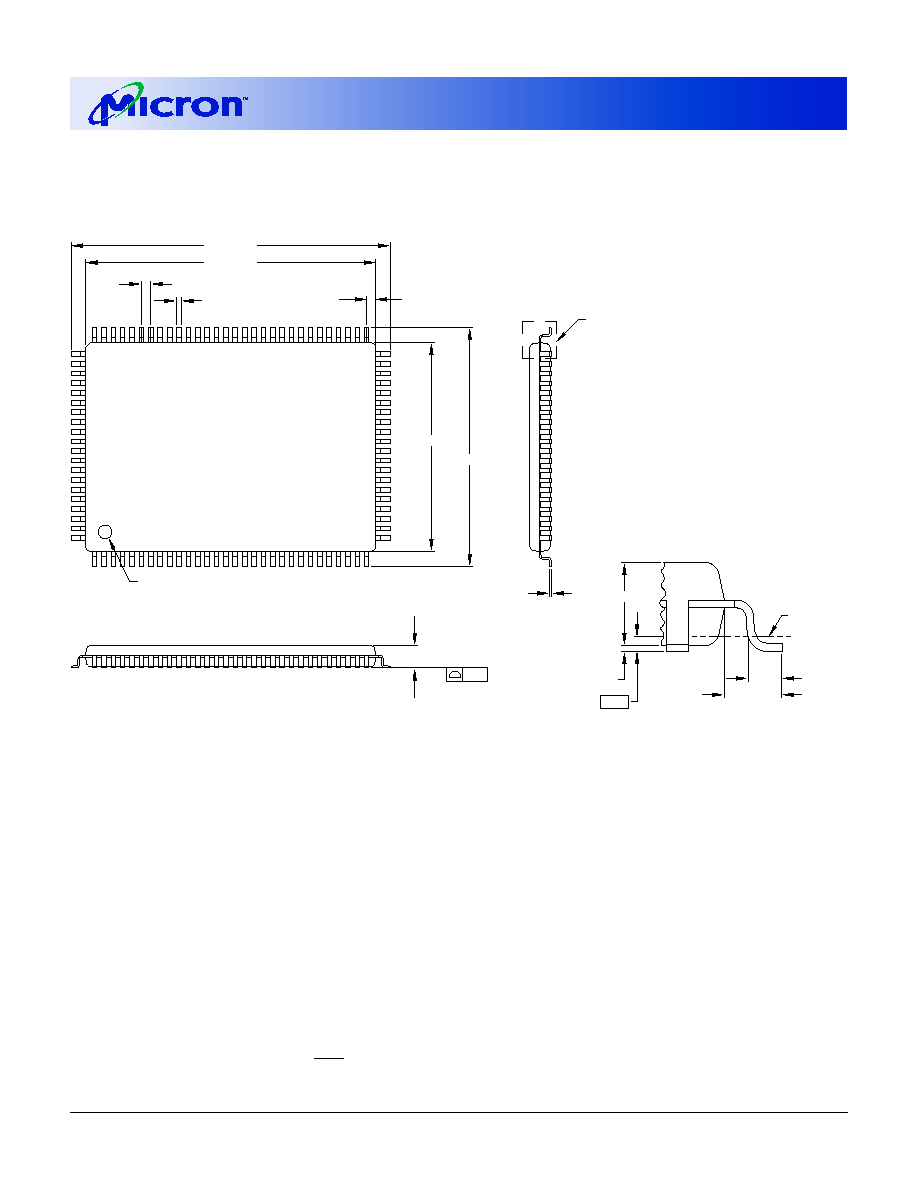
41
18Mb: 1 Meg x 18, 512K x 32/36 Flow-Through SyncBurst SRAM
Micron Technology, Inc., reserves the right to change products or specifications without notice.
MT58L1MY18F_C.p65 ≠ Rev. C, Pub. 9/01
©2001, Micron Technology, Inc.
18Mb: 1 MEG x 18, 512K x 32/36
FLOW-THROUGH SYNCBURST SRAM
ADVANCE
100-PIN PLASTIC TQFP (JEDEC LQFP)
14.00 ±0.10
1.40 ±0.05
16.00 ±0.20
0.10
+0.10
-0.05
0.15
+0.03
-0.02
22.10
+0.10
-0.20
0.32
+0.06
-0.10
20.10 ±0.10
0.65 TYP
0.62
1.60 MAX
DETAIL A
SEE DETAIL A
0.60 ±0.15
0.60 ±0.15
1.00 TYP
GAGE PLANE
0.10
0.10
PIN #1 ID
NOTE: 1. All dimensions in millimeters MAX or typical where noted.
MIN
2. Package width and length do not include mold protrusion; allowable mold protrusion is 0.25mm per side.
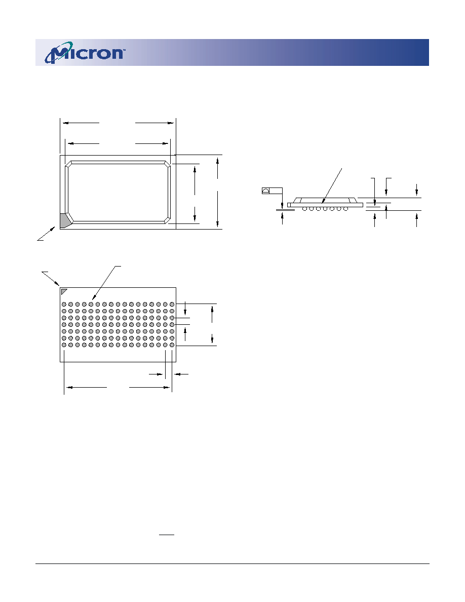
42
18Mb: 1 Meg x 18, 512K x 32/36 Flow-Through SyncBurst SRAM
Micron Technology, Inc., reserves the right to change products or specifications without notice.
MT58L1MY18F_C.p65 ≠ Rev. C, Pub. 9/01
©2001, Micron Technology, Inc.
18Mb: 1 MEG x 18, 512K x 32/36
FLOW-THROUGH SYNCBURST SRAM
ADVANCE
ÿ
7.62
20.32
19.94 ±0.10
11.94 ±0.10
1.27 (TYP)
1.27 (TYP)
0.60 ±0.10
2.40 MAX
0.90 ±0.10
14.00 ±0.10
22.00 ±0.20
A1 CORNER
A1 CORNER
(dimension applies to a
noncollapsed solder ball)
Substrate material:
BT resin laminate
0.15
SEATING PLANE
0.75 ±0.15
NOTE: 1. All dimensions in millimeters MAX or typical where noted.
MIN
2. Solder ball land pad is 0.6mm.
119-PIN BGA

43
18Mb: 1 Meg x 18, 512K x 32/36 Flow-Through SyncBurst SRAM
Micron Technology, Inc., reserves the right to change products or specifications without notice.
MT58L1MY18F_C.p65 ≠ Rev. C, Pub. 9/01
©2001, Micron Technology, Inc.
18Mb: 1 MEG x 18, 512K x 32/36
FLOW-THROUGH SYNCBURST SRAM
ADVANCE
165-PIN FBGA
NOTE: 1. All dimensions in millimeters MAX or typical where noted.
MIN
10.00
14.00
15.00 ±0.10
1.00
TYP
1.00
TYP
5.00 ±0.05
13.00 ±0.10
PIN A1 ID
PIN A1 ID
BALL A1
MOLD COMPOUND: EPOXY NOVOLAC
SUBSTRATE: PLASTIC LAMINATE
6.50 ±0.05
7.00 ±0.05
7.50 ±0.05
1.20 MAX
SOLDER BALL MATERIAL: EUTECTIC 63% Sn, 37% Pb
SOLDER BALL PAD: ÿ .33mm
SOLDER BALL DIAMETER REFERS
TO POST REFLOW CONDITION. THE
PRE-REFLOW DIAMETER IS ÿ 0.40
SEATING PLANE
0.85 ±0.075
0.12 C
C
165X ÿ 0.45
BALL A11
8000 S. Federal Way, P.O. Box 6, Boise, ID 83707-0006, Tel: 208-368-3900
E-mail: prodmktg@micron.com, Internet: http://www.micron.com, Customer Comment Line: 800-932-4992
Micron is a registered trademark and the Micron logo and M logo are trademarks of Micron Technology, Inc.
SyncBurst is a trademark and Micron is a registered trademark of Micron Technology, Inc.
Pentium is a registered trademark of Intel Corporation.

44
18Mb: 1 Meg x 18, 512K x 32/36 Flow-Through SyncBurst SRAM
Micron Technology, Inc., reserves the right to change products or specifications without notice.
MT58L1MY18F_C.p65 ≠ Rev. C, Pub. 9/01
©2001, Micron Technology, Inc.
18Mb: 1 MEG x 18, 512K x 32/36
FLOW-THROUGH SYNCBURST SRAM
ADVANCE
REVISION HISTORY
Rev. C, Pub. 9/01, ADVANCE ................................................................................................................................ Sept/01
∑ Removed Industrial Temperature references
∑ Changed I
DD
tables by splitting x18 and x32/36 configuration
∑ Changed NC references to NF
∑ Removed note "Not Recommended for New Design" from 119-pin FBGA
∑ Changed boundary scan order, 165-pin FBGA, x18 and x32/36
8P (SA) moved to bit #9 from bit #3
∑ Increased I
DD
table values
Rev. 2/01, ADVANCE ...................................................................................................................................................... Feb/24/01
∑ Added Industrial Temperature references
Rev. 1/01, ADVANCE ....................................................................................................................................................... Jan/10/01
∑ Added 165-pin FBGA 5ta6 Scan Order
∑ Added 119-pin PBGA package and references
Rev. 8/00, ADVANCE ...................................................................................................................................................... Aug/22/00
∑ Removed FBGA Part Marking Guide
Rev. 7/00, ADVANCE ........................................................................................................................................................ Aug/8/00
∑ Changed FBGA capacitance values
∑ C
I
; TYP 2.5 pF from 4 pF; MAX 3.5 pF from 5 pF
∑ C
O
; TYP 4 pF from 6 pF; MAX 5 pF from 7 pF
∑ C
CK
; TYP 2.5 pF from 5 pF; MAX 3.5 pF from 6 pF
Rev. 7/00, ADVANCE ..................................................................................................................................................... July/24/00
∑ Removed Industrial Temperature referencesJuly/24/00
Rev. 7/00, ADVANCE ..................................................................................................................................................... Jun/28/00
∑ Added 165-pin FBGA package
∑ Added FBGA part marking references
∑ Removed 119-pin PBGA and references
∑ Added note: "IT available for -8.5 and -10 speed grades"
Rev. 4/00, ADVANCE ...................................................................................................................................................... Apr/13/00
∑ Change pin 14 to NC from V
DD
∑ Added note: ZZ has internal pull-down
Rev. 3/00, ADVANCE ........................................................................................................................................................ Apr/6/00
∑ Updated Boundary Scan Order
Rev. 1/00, ADVANCE ....................................................................................................................................................... Jan/18/00
∑ Added ADVANCE status
Rev. 11/99, ADVANCE ................................................................................................................................................... Nov/11/99
∑ MT58L1MY18F
∑ Added BGA JTAG functionality