 | –≠–ª–µ–∫—Ç—Ä–æ–Ω–Ω—ã–π –∫–æ–º–ø–æ–Ω–µ–Ω—Ç: DMA2286 | –°–∫–∞—á–∞—Ç—å:  PDF PDF  ZIP ZIP |

DMA 2275,
DMA 2286
C/D/D2-MAC
Descrambler
Edition May 20, 1992
6251-330-1E
MICRONAS
INTERMETALL
MICRONAS

DMA 2275, DMA 2286
2
Contents
Page
Section
Title
4
1.
Introduction
4
1.1.
General Information
4
1.2.
Environment
5
2.
Chip Architecture
6
3.
Video Processor
6
3.1.
Code Converter
6
3.2.
Video Descrambler
6
3.3.
Interpolation Filter
6
3.4.
Clamping and Video Gate
7
4.
PRBS Generator
7
4.1.
Video PRBS Generator
7
4.2.
Packet PRBS Generator
7
4.3.
VBI Descrambler
8
5.
Line 625 Processor
8
5.1.
Majority Decision
8
5.2.
BCH Check
8
5.3.
Frame Counter Flywheel
8
5.4.
RTCI Detector
9
6.
Sound Processor
9
6.1.
The S Bus Interface and the S Bus
10
7.
Packet Processor
10
7.1.
Packet Acquisition
11
7.2.
Packet Descrambler
12
8.
Interface Processor
12
8.1.
Fast Processor
13
8.2.
IM Bus Interface
13
8.2.1.
IM Bus Addresses and Instructions
18
8.3.
DRAM Interface
19
8.4.
DRAM Memory Map
19
8.4.1.
Mode Register
20
8.4.2.
Pac1 Register
21
8.4.3.
Pac2 Register
23
8.4.4.
Coeff Register
24
8.4.5.
CW Register
25
8.4.6.
Error Buffer
26
8.4.7.
Packet Buffer
28
8.4.8.
Line 625 Buffer
29
8.4.9.
Scratch Buffer
29
8.5.
FP Memory Map

DMA 2275, DMA 2286
3
Contents, continued
Page
Section
Title
31
9.
Specifications
31
9.1.
Outline Dimensions
31
9.2.
Pin Connections
34
9.3.
Pin Configuration
34
9.4.
Pin Descriptions
35
9.5.
Pin Circuits
36
9.6.
Electrical Characteristics
36
9.6.1.
Absolute Maximum Ratings
37
9.6.2.
Recommended Operating Conditions
39
9.6.3.
Characteristics
40
9.6.4.
Sound DRAM Interface Characteristics
42
9.6.5.
Acquisition DRAM Interface Characteristics
44
9.6.6.
Waveforms
46
10.
References

DMA 2275, DMA 2286
4
The DMA 2275 and DMA 2286 C/D/D2≠MAC De-
scrambler
1. Introduction
1.1. General Information
The DMA 2275 is a digital real≠time descrambling pro-
cessor for the D2≠MAC/Packet system. Together with
the D2≠MAC/Packet decoder chip DMA 2271, it can be
used to build up a D2≠MAC/Packet conditional access
receiver.
The DMA 2286 is a digital real≠time descrambling pro-
cessor for the C/D/D2≠MAC/Packet system. Together
with the C/D/D2≠MAC/Packet decoder chip DMA 2281,
it can be used to build up a C/D/D2≠MAC/Packet condi-
tional access receiver.
The programmable VLSI circuits in CMOS technology
are housed in 68≠pin packages and contain on a single
silicon chip the following functions:
DMA 2275 and DMA 2286
≠ descrambling of MAC video signal
≠ interpolation of MAC video signal (aspect ratio 16:9)
≠ descrambling of MAC data packets
≠ descrambling of VBI≠teletext
≠ entitlement packet acquisition
≠ supplementary general purpose packet acquisition
≠ line 625 acquisition
≠ communication with external microprocessor via the
IM bus
DMA 2286 only
≠ one subframe sound processing C/D/D2≠MAC
1.2. Environment
Figures 1≠1 and 1≠2 show how the descrambler chips
DMA 2275 and DMA 2286 can be implemented into a
MAC conditional access receiver together with other cir-
cuits of ITT's DIGIT 2000 digital TV system. These re-
ceivers provide descrambling facility for one video ser-
vice and up to four audio or data services including
VBI≠teletext. It is important to notice that the DMA 2275
or DMA 2286 do not include any decryption or security
functions. These functions will be carried out by one or
more conditional access subsystems (CASS) which
communicate with the descrambler chip via the central
control unit (CCU) and the IM bus.
D2MAC
Baseband
Signal
CASS
VCU 2133
A/D Part
MCU 2600
NVM 3060
DRAM
DMA 2271
VCU 2133
D/A Part
AMU 2481
R
G
B
S1
S2
S3
S4
Fig. 1≠1: Block diagram for a stand≠alone D2≠MAC
decoder
TPU 2735
DRAM
DMA 2275
DRAM
CCU 3000
CASS
VCU 2133
A/D Part
MCU 2600
NVM 3060
DRAM
DMA 2281
VCU 2133
D/A Part
AMU 2481
R
G
B
S1
S2
S3
S4
TPU 2740
DRAM
DMA 2286
DRAM
CCU 3000
D/D2MAC
Baseband
Signal
DRAM
Fig. 1≠2: Block diagram for a stand≠alone D/D2≠
MAC decoder

DMA 2275, DMA 2286
5
2. Chip Architecture
Figure 2≠1 shows the architecture of the descrambling
chip DMA 2286. The DMA 2275 architecture is identical
to the that of the DMA 2286, except that the sound pro-
cessor is missing. The chips can be subdivided into sev-
eral functional blocks.
DMA 2275 and DMA 2286:
Video Processor
≠ descrambling, panning and interpolation of the video
signal
PRBS Generator
≠ delivers cut points and cipher streams
Line 625 Processor
≠ acquisition of service identification data and real time
control information
Packet Processor
≠ acquisition of entitlement packets, acquisition of gen-
eral purpose packets, selection of cipher stream, des-
crambling of data packets
Interface Processor
≠ management of internal and external data transfer
Timing Generator
≠ delivers internal chip timing
DMA 2286 only:
Sound Processor
≠ spectrum descrambling of data burst, packet deinter-
leaving (one subframe only), sound packet processing
(one subframe only)
Line 625 Proc.
3
Vdd
Vdd
GND
GND
Fig. 2≠1: Block diagram of the DMA 2286
PRBS Generator
Video Processor
Interface Processor
Timing
Generator
Sound
Proc.
Packet Processor
Code
Converter
Video
Descrambler
Interpolation
Filter
Clamping +
Video Gate
Video
PRBS
Generator
Packet
PRBS
Generator
Fast
Processor
IM Bus
Interface
DRAM
Interface
Timing
Generator
Packet
Acquisition
Line 625
Acquisition
Packet
Descrambler
Spectr. Descr.
Deinterleaver
Sound
Processing
Baseband
Addr
.
RAS
CAS
R/W
Data
IM Bus
Busy
Reset
M
Burst
Sync
DRAM
S Bus
Audio
Clock
8
8
8
8
Burst
Data
12
2
Packet
Data
Descrambl.
Packet
Data
Corrected
Packet
Data
VBI
Data
Baseband
8
8
8

DMA 2275, DMA 2286
6
3. Video Processor
The video processor consists of:
≠ Code Converter
≠ Video Descrambler
≠ Interpolation Filter
≠ Clamping and Video Gate
3.1. Code Converter
Input for the video processor is the digitized baseband
signal which may be delivered by the VCU 2133 in paral-
lel Gray code or by the UVC 3130 in simple binary code.
Therefore, a code converter from Gray to binary code is
intended. This converter can be disabled under software
control (bit 6 of video mode register) and can be
switched from 7 to 8 bit input (test bit TT6).
3.2. Video Descrambler
To make the transmitted video signal unintelligible, the
luma and/or chroma component are cut into two seg-
ments in the MAC encoder. These two segments are
then transposed. Task of the video descrambler is to re-
transpose the segments into their original waveform.
Three different video waveforms are possible:
≠ clear
≠ double≠cut component rotation
≠ single≠cut line rotation
The video descrambler has to cope with all these video
waveforms. In any case the output signal has a constant
delay of 1296 + 4 clock periods in order to avoid synchro-
nization problems during change of the video scram-
bling mode. For any video configurations not corre-
sponding to Fig. 3, part 2, p. 75 of ref. 1, the video
descrambler should be disabled by the software. The
signal is then passed through the descrambler unaf-
fected except for the delay of one line.
The baseband data burst signal passes the video des-
crambler through a special shift register, luma and chro-
ma rotation is done in within two video RAMs. The video
RAMs are subdivided into chroma and luma segments
which are organized as ringbuffer. The concerning ad-
dress counter is loaded every line with a start value de-
pending on the cut point (CPL or CPC) in case of scram-
bling, on the pan vector (PANV) in case of 16:9 aspect
ratio and in any case on an offset value which is pro-
grammable (FP register 33 and 34). The calculation of
the start address is done by the Fast Processor in real
time. The expansion of the compatible 4:3 part in case
of 16:9 aspect ratio is done by reading every third sam-
ple twice.
3.3. Interpolation Filter
If the compatible 4:3 part of a 16:9 picture is to be pro-
cessed (see Fig. 7, part 2, p. 79 of ref. 1), only this part
of the luma and chroma component is read out of the vid-
eo memory (262 chroma samples, 523 luma samples).
An interpolation filter is then used to regain the number
of samples expected by the DMA 2271 or DMA 2281
(349 chroma samples, 697 luma samples). The sam-
pling rate ratio is 4:3. The filter function is defined by a
set of 16 coefficients, which are programmable. Down-
load of these coefficients into the interpolation filter is a
one shot function triggered by software (bit 4 of vid-
eo_mode register).
The interpolation is not influenced by the video scram-
bling method, because the output signal of the video
memory appears unscrambled. The position of the com-
patible 4:3 part is programmable so that user panning is
possible. The panning can also be controlled by the
broadcaster when sending real time pan vectors in line
625. The selection of these two panning modes is done
by bit 7 of the scram_mode registers.
The high frequency losses in the interpolation filter can
be partly compensated with a peaking filter. Low peaking
increases the signal level about 6 dB at 5 MHz, high
peaking increases the signal level about 10 dB at 5 MHz.
Peaking is controlled with bit 0 and 1 in the video_mode
register.
Alternatively the interpolation and peaking filter can be
used for baseband filtering. It is then enabled not only
during active video, but also during the data burst and
VBI transmission. The filter coefficients have to be
changed for this application.
3.4. Clamping and Video Gate
The DC level of the analog baseband signal is controlled
by the clamping circuit of the DMA 2271 or DMA 2281
decoder chip which measures the clamping period of
each line. The line store in the video descrambler of the
DMA 2275 or DMA 2286 would cause a line delay within
the clamping control loop with all corresponding prob-
lems.
Therefore, the line store of the descrambler chip is by-
passed during the clamping period to avoid the line
delay. The position of the clamping bypass within the line
can be programmed in steps of 99 clock cycles (bit 3≠0
in mac_mode register). Clamp position `0' would be lo-
cated after the first subframe of a D≠MAC signal. Clamp
position `1' is the default specified in ref 1. The clamp by-
pass is automatically disabled in line 625 and line 1.
Finally, a video gate is provided to switch the luminance
component to black and the chrominance component to
zero in case of denied access to the video service. This
gate can be used in country by country control (CbCC)
applications to black out special programs under soft-
ware control (bit 5 of video_mode register).

DMA 2275, DMA 2286
7
4. PRBS Generator
The PRBS generator delivers pseudo random binary se-
quences to descramble the video signal, packet data,
and VBI data. It consists of:
≠ Video PRBS Generator
≠ Packet PRBS Generator
4.1. Video PRBS Generator
The Video PRBS generator delivers the cut points for the
luma and chroma component as two bytes per line (CPL
and CPC). These two bytes are calculated in the PRBS
2 generator described in detail in Fig. 4, part 6, p. 205
and Fig. 3, appendix to part 6, p. 309 of ref. 1.
The PRBS 2 generator is clocked 16 times at the begin-
ning of each line in a way that the cut points are available
before start of the vision signal. The PRBS 2 generator
is loaded with a 60 bit video initialization word (VIW) at
the beginning of each frame. The video initialization
word is a combination of the 8 bit frame counter (FCNT)
and a 60 bit video control word (VCW) which is either one
of the local control words (LCW_even and LCW_odd) or
one of the video control words received from the CASS
(VCW_even and VCW_odd).
The selection of even or odd control words is done with
the LSB of the conditional access frame counter
(CAFCNT). CAFCNT and FCNT are delivered by the
line 625 processor. All control words (including the local
control words) are read out of the control word registers
of the external acquisition DRAM. These registers must
be defined by CCU software, which gets control words
from the CASS and initializes the local control words
with all bits set to `1'.
4.2. Packet PRBS Generator
The packet PRBS generator delivers the descrambling
sequence for four different data channels which may
carry sound or teletext or any other data service. The se-
quence is used to descramble the 720 useful data bits
(after packet header and PT≠byte) of packets carrying
a scrambled service component.
The packet PRBS generator consists of four PRBS 1
generators and four PRBS 3 generators described in de-
tail in Fig. 3, part 6, p. 203, Fig. 5, part 6, p. 207, Fig. 2,
appendix to part 6, p. 308 and Fig. 4, appendix to part 6,
p. 310 of ref. 1.
The four data initialization words (DIW) for the PRBS 1
generators are derived in the same way as in the video
PRBS generator and are loaded at the beginning of each
frame. Each PRBS 1 generator is then clocked 61 times
before receiving the next data packet and the serial out-
put, called packet initialization word (PIW), is loaded into
the PRBS 3 generator.
The actual descrambling sequence is generated in one
of the PRBS 3 generators which is selected by the pack-
et recognition each time a scrambled packet arrives.
Channel 1 of the packet recognition selects the PRBS 3
generator which is loaded from the PRBS 1 generator
initialized with DCW1 and so on.
4.3. VBI Descrambler
Although there is no specification of VBI descrambling
in ref. 1, the DMA 2275 or DMA 2286 provide means of
descrambling VBI data in a simple manner.
The PRBS 1 generator for channel 4 can be used to des-
cramble 2≠4 PSK demodulated or duobinary decoded
data in the VBI (e.g. VBI≠teletext). In this case the PRBS
1 generator will be clocked with 10.125 MHz (D2≠MAC)
or 20.25 MHz (C/D≠MAC) and its serial output is directly
used to descramble the VBI data burst. The VBI_PRBS
starts with bit 117 and stops after bit 648 (D2≠MAC) or
bit 1296 (D≠MAC) of each data burst of the VBI. The VBI
is defined from line 1 to 22 and line 311 to 334 inclusive.
Due to the fast processor software (see Fig. 8≠1), the
PRBS 1 generator can only be loaded in line 7. This
means that the VBI descrambler operates from line 1 to
line 6 with the data initialization word (DIW) of the pre-
vious frame. During line 7 the VBI data output (pin 20)
is unpredictable.
The delay between data burst input (pin 19) and des-
crambled VBI data output (pin 20) is 4 clock periods.

DMA 2275, DMA 2286
8
5. Line 625 Processor
The line 625 processor is loaded via the data burst input.
Line 625 is identified by checking the sync pulse of the
data burst input. The normal sync pulse covers only 6
bits of the line synchronization word (LSW), the sync
pulse of line 625 covers 102 bits of the frame synchroni-
zation data (FSD) and is directly followed by:
≠
5 bit
≠
71 bit
≠ 470 bit
UDT
SDF
RDF
unified data time
static data frame
repeated data frame
546 bit
line 625 data
In case of C≠MAC or D≠MAC the 546 bits of UDT, SDF
and RDF are interleaved with PRBS data. The PRBS
data are discarded by using a clock divider so that the
clock frequency for the line 625 processor is unique for
C≠, D≠ and D2≠MAC (10.125 MHz). UDT, SDF and the
error corrected TDMCTL data are stored into the exter-
nal acquisition DRAM (see figure "Line 625 Buffer") and
are updated every frame.
The line 625 processor consists of:
≠ Majority Decision
≠ BCH Check
≠ Frame Counter Flywheel
≠ RTCI Detector
5.1. Majority Decision
The RDF consists of five successive identical 94 bit data
blocks transmitting time division multiplex control
(TDMCTL) information. The fivefold repetition is used by
a 3 of 5 majority decision including the BCH suffix.
5.2. BCH Check
SDF and TDMCTL are each protected by a 14 bit BCH
suffix. The BCH check is only used for error detection.
BCH check for the TDMCTL is done after majority deci-
sion. The complete SDF (71 bit) or TDMCTL (94 bit) in-
formation is stored into DRAM together with two error
flags SDF_Error and TDM_Error indicating the result of
the BCH check.
5.3. Frame Counter Flywheel
The 8 bit frame counter (FCNT) is used in conjunction
with the PRBS generators of the descrambling system.
The correct acquisition of FCNT is essential to maintain
a scrambled service. Therefore, a flywheel technique is
used in a way that a free running frame counter is syn-
chronized from time to time with the received FCNT in
line 625. In this case even the loss of several line 625
data will not disturb the service acquisition.
The CAFCNT LSB is used to select even and odd control
words and allows frame accurate switching from one
phase to the other. Therefore, a similar flywheel tech-
nique is used to protect this LSB. In fact, the internal
CAFCNT LSB is the 9th bit of the free running frame
counter and is synchronized by the actually transmitted
CAFCNT LSB after a majority decision over several
frames.
5.4. RTCI Detector
A special TDMCID code in the TDMCTL indicates the
presence of real time control information (RTCI) trans-
mitted instead of TDMS and LINKS. TDMCID = `81'
(hex) is defined to signal the transmission of real time
panning information.
The pan vector PANV is needed for panning the 4:3 por-
tion of a 16:9 picture. In this case the 63 bits of TDMS
and LINKS are substituted with 56 bits of PANV. PANV
is organized in seven bytes giving the pan vector for
seven consecutive frames starting from the second
frame after transmission. Each byte of PANV defines in
2's complement format the offset of the 4:3 portion from
the center position (see Fig. 7, part 2, p. 79 of ref. 1).
After detection of TDMCID = `81' (hex) the following
seven bytes are stored in a FIFO which is read out once
a frame with one frame delay. If the FIFO is empty the
last byte will be repeated until a new pan vector is re-
ceived. The TDMCTL transmitting the pan vector will be
stored into the line 625 buffer like any other TDMCTL in-
formation.
If user panning is selected by software, the pan vector
inside TDMCID will be ignored and a user defined pan
vector will be used instead, allowing the user to pan the
picture himself. In any case the recently transmitted pan
vector in line 625 is stored in the pan output register to
allow the software to make a smooth return between dif-
ferent pan positions.

DMA 2275, DMA 2286
9
6. Sound Processor
The DMA 2286 contains an additional sound processor,
which is loaded via the data burst input. The sound pro-
cessor consists of:
≠ spectrum descrambler
≠ deinterleaver
≠ sound processing
≠ S Bus interface
These blocks are identical to the sound processing
blocks of the DMA 2281 (see ref. 2). Both sound proces-
sors are able to decode 4 sound channels out of one
single subframe. The subframe position is program-
mable to allow full channel data reception.
On the DMA 2286 the output of the deinterleaver is inter-
nally fed to the packet descrambler and the des-
crambled packets are going back to the sound proces-
sor.
The sound processor needs a separate external
64 k x 1 bit DRAM, which is independent from the acqui-
sition DRAM and is not accessible by software.
6.1. The S Bus Interface and the S Bus
The S bus has been designed to connect the digital
sound output of the DMA 2271 or DMA 2281 MAC De-
coder or the MSP 2400 NICAM Demodulator/Decoder to
audio≠processing ICs such as the AMU 2481 Audio Mix-
er or the ACP 2371 Audio Processor etc., and to connect
these ICs one to the other. The S bus is a unidirectional,
digital bus which transmits the sound information in one
direction only, so that it is not necessary to solve priority
problems on the bus.
The S bus consists of the three lines: S≠Clock, S≠Ident,
and S≠Data. The DMA 2271, DMA 2281 or the MSP
2400 generates the signals S≠Clock and S≠Ident, which
control the data transfer to and between the various pro-
cessors which follow the DMA 2271, DMA 2281 or the
MSP 2400. For this, the S≠Clock and S≠Ident inputs of
all processors in the system are connected to the S≠
Clock and S≠Ident outputs of the DMA 2271, DMA 2281
or the MSP 2400. S≠Data output of the DMA 2271, DMA
2281 or MSP 2400 is connected to the S≠Data input of
the next following AMU, the AMU's S≠Data output is
connected to the ACP's S≠Data input and so on.
The sound information is transmitted in frames of 64 bits,
divided into four successive 16≠bit samples. Each sam-
ple represents one sound channel. The timing of a com-
plete transmission of four samples is shown in Fig. 9≠13,
the times are specified under "Recommended Operat-
ing Conditions". The transmission starts with the LSB of
the first sample. The S≠Clock signal is used to write the
data into the receiver's input register. the S≠Ident signal
marks the end of one frame of 64 bits and is used as latch
pulse for the input register. The repetition rate of S≠Ident
pulses is identical to the sampling rate of the D/D2≠MAC
or NICAM sound signal; thus it is possible to transfer four
sound channels simultaneously.
The S bus interface of the DMA 2286 mainly consists of
an output register, 64≠bit wide. The timing to write bit by
bit is supplied by the Audio≠Clock signal. In the case of
an S≠Ident pulse, the contents of the output register are
written to the S≠Data output.
The S_Bus_Data line of the DMA 2286 can be con-
nected to that of the DMA 2281 if only one audio proces-
sor AMU 2481 is available. In this case each S_Bus
channel of both DMA chips can be enabled or disabled
under software control.

DMA 2275, DMA 2286
10
7. Packet Processor
The packet processor is loaded via the scrambled pack-
et data input with packets of one subframe delivered by
the DMA 2271 or DMA 2281 and additionally has an in-
ternal connection to the deinterleaver of the DMA 2286
for packets of the other subframe. Packet data on these
lines are already spectrum descrambled and deinter-
leaved. The packet header and the PT byte have already
been corrected. The transmission of each packet starts
with a `0' bit followed by 751 bit packet data with a unique
bit rate of 10.125 MHz (for C≠, D≠ and D2≠MAC).
To avoid simultaneous reception of two packets from dif-
ferent subframes, the packet output of the DMA 2286
has to be delayed in reference to the packet output of the
DMA 2281. This can be done with the CD bit in IM_Bus
register 197.
The packet processor consists of:
≠ Packet Acquisition
≠ Packet Descrambler
7.1. Packet Acquisition
Task of the packet acquisition is to select specific pack-
ets out of the packet multiplex. In case of C≠ or D≠MAC
packets can be located in one or two subframes, there-
fore, the packet selection will be repeated in the second
subframe if necessary. The selected packets can be er-
ror corrected if needed and are stored into packet buff-
ers which are located in the acquisition DRAM.
Due to timing conflicts with the line 625 acquisition, it is
not possible to acquire packets in the last (82nd) packet
slot of each subframe.
Additionally, all packets of both subframes are available
on a separate output pin (corrected packet data output),
only that the selected packets are replaced by their error
corrected equivalents.
The most common application of the packet acquisition
will be the selection of the following packets:
≠ `0' packets
≠ EMM packets
≠ ECM packets
≠ BI packets
≠ 2nd level teletext packets
≠ general purpose data packets
The `0' packets are forming the service identification (SI)
channel. The first thing the receiver software has to do
is to monitor the SI channel and to configure the receiver
according to the SI information. `0' packets are either
hamming protected (H[8,4]) or golay protected (Golay
[24,12]). The SI channel is subdivided into 16 data
groups which can be identified by the data group (TG)
byte immediately following the PT byte of the packet
header.
The EMM and ECM packets are essentially carrying en-
cryption keys and control words. Their packet addresses
are indicated by the LISTX, ACMM and ACCM parame-
ters of the service identification channel. EMM packets
can be addressed to a single customer or a group of cus-
tomers by means of an address extension field of up to
36 bit, immediately following the PT byte. EMM and
ECM packets are highly error protected (Golay [24,12]
or Hamming [8,4]).
BI packets are carrying additional interpretation data re-
lated to sound packets with the same packet address.
They are selected by their PT byte (`00' or `3F'). BI pack-
ets are not error corrected.
Second level teletext packets can be selected to do
Golay [24,12] correction. They are available then on the
corrected packet data output which can be connected to
the teletext processor TPU 2740.
Every selected packet is CRC checked regardless of
packet type and error protection. The CRC check is
done over the full range of 720 bit and does not change
any packet data. CRC check, Golay [24,12] and Ham-
ming [8,4] error correction is done in real time, i.e. with
10.125 MHz. In case of packets with Golay [24,12] error
protection, the protection bits will be removed before
storing these packets into the packet buffer. the packet
length is therefore reduced from 96 bytes (full length
packet) to 48 bytes (half length packets), doubling the
possible number of packets in the related packet buffer.
The result of CRC check and the number of uncorrect-
able Golay or Hamming codes per packet is indicated in
a special packet error buffer which holds up to 16 error
bytes for every packet buffer. In case of full length pack-
ets, only every second entry of the error buffer is used.
Every selected packet is stored into the external acquisi-
tion DRAM of the descrambler chip. The DRAM includes
8 independent packet buffers, each offering the data ca-
pacity to store 8 full length packets or 16 half length
packets. The packet buffers can be read out by software
at any time and in any sequence. There are two ways to
use these packet buffers. One is the "standard" buffer
application where the buffer is automatically closed
when it is filled up with packets. The buffer must then be
reopened by software to start packet acquisition again.
The second way is the "ring" buffer application where the
packet buffer is always open and the oldest packets in
the buffer are overwritten by the next incoming packets.
Each packet buffer can be monitored by reading its buff-
er status. The buffer status is located in the FP memory
and includes a buffer pointer (bit 4≠0) which indicates
the position where the next packet will be stored in num-
bers of half length packets. In ring buffer application this
pointer runs modulo 16 and in standard buffer applica-
tion the pointer stops at 16.

DMA 2275, DMA 2286
11
The buffer application (standard/ring) can be defined
with bit 5 in the buffer status register. Bit 7 allows to close
or reopen the buffer under software control. Bit 6 defines
the buffer increment. that means whether the buffer will
store full length (96 byte) packets or half length (48 byte)
packets.
Each of the 8 packet buffer is attached to a program-
mable packet filter which selects specific packets out of
the packet multiplex depending on packet address (PA),
continuity index (CI), packet type (PT) and packet ad-
dress extension (PAE). The packet address extension
can be used to select EMM packets by their specific cus-
tomer address (UCA, SCA, CCA) or to select ECM pack-
ets by command identification (CI or to select the data
group type (TG) of `0' packets. This selection is done af-
ter error correction.
Each of the 8 packet filter is controlled by a set of regis-
ters located in the acquisition DRAM and programmable
by software. The `packet address base' (PAB) registers
define the 10 bit packet address and the continuity in-
dex. The `packet address extension' (PAE) registers de-
fine up to 36 bit of the address extension field. The `pack-
et selection control' (PSC) registers define how packets
will be selected, error corrected and linked together.
The software should take care of conflicts like program-
ming different packet filters with the same conditions.
There must be at least one difference in the combination
of packet address, continuity index, packet type, and
packet location. Otherwise the result of the packet selec-
tion will be undefined.
If packet link is activated, the first packet meeting all pro-
grammed conditions is defined as sync packet. Selec-
tion of continuation packets is done according to the
packet link status. In case of CI link, the continuity index
of following packets will be ignored. In case of PT link,
the packet type selection is changed to PT2. a special bit
in the buffer status indicates if this procedure has been
activated by the first sync packet. The packets are then
stored into the packet buffer in the same order as they
are transmitted. The choice of packet link is independent
from the choice of buffer application.
Depending on the page select bit in the PSC register the
packet address extension is checked in every packet or
only in the sync packet. To select linked EMM packets by
customer address this bit should be `0', to select linked
`0' packets by data group type this bit should be `1'.
7.2. Packet Descrambler
Main task of the packet descrambler is to detect those
sound or data packets that have to be descrambled.
Four different packet addresses can be recognized. Af-
ter detection of such a packet the concerning PRBS 3
generator is selected and produces an output sequence
of 720 bit to descramble the packet data. The PT≠Byte
of each selected packet is decoded to disable the PRBS
3 generator output in case of BI packets (`00' or `3F').
The packet descrambler can be switched to "automatic"
operation. In this mode the 4 center bits of the packet ad-
dress are ignored by the packet address comparator.
In case of C≠ or D≠MAC, packets carrying one digital
component can be inserted in one or both subframes,
therefore the packet recognition will be repeated in the
second subframe if necessary.
Because the packet header is not scrambled, the packet
recognition has about 20 clock cycles to compare the
packet address before start of the descrambling se-
quence. Therefore there is only a 4 clock cycle delay be-
tween packet input and output.
Additionally, a packet gate is provided to remove pack-
ets form the packet output in case of denied access to
that particular service. These packets are not physically
removed ≠ only the 720 bits after the packet header are
set to `1'.
Any other packet not selected by the packet recognition
passes through the packet descrambler unaffected but
with a delay of 4 clock periods.
The packet recognition is controlled by a set of registers
located in the acquisition DRAM and programmable by
software. The `scrambled packet address' (SPA) regis-
ters define the 10 bit packet address and the `scrambled
packet status' (SPS) registers define packet location
and status.
The software should take care of conflicts like program-
ming different SPA and SPS registers in the combination
of packet address and packet location. Otherwise, the
result of the packet recognition will be undefined.

DMA 2275, DMA 2286
12
8. Interface Processor
The interface processor consists of:
≠ Fast Processor
≠ IM Bus Interface
≠ DRAM Interface
8.1. Fast Processor
The fast processor (FP) is a RISC≠type 12 bit microcon-
troller built in CMOS technology. The maximum clock
frequency of 40 MHz and the internal architecture that
allows parallel ALU operation and data transfer to or
from internal RAM, make it applicable for very high
speed tasks, such as control and parameter calculation
in digital signal processors.
The FP is embedded in the DMA 2275 or DMA 2286 with
256 x 12 bit RAM and 2K x 20 bit ROM and runs with
20.25 MHz. The FP performs the following tasks:
≠ data transfer to and from DRAM interface
≠ data transfer to and from IM Bus interfaces
≠ support of packet acquisition
≠ support of line 625 acquisition
≠ initialization of PRBS generators
≠ control of video descrambler
≠ control of interpolation filter
Fig. 8≠1 shows roughly when the different FP tasks are
executed within a frame period.
In normal operation the FP will not be directly accessed
from outside, that means that the CCU software will not
see another processor on the descrambling chip but
only a set of registers and buffers which are located ei-
ther in the acquisition DRAM or in the FP internal
memory. The CCU can access both memories via IM
Bus.
Changing any register in the DRAM memory by CCU
software will not effect the descrambler hardware im-
mediately. The FP will read or update the DRAM
memory only on frame boundaries, i.e. from line 622 to
line 7 inclusive. Changing registers in the FP memory by
CCU software will effect the descrambler hardware im-
mediately.
line_sync
prbs2
manager
line_625_store
line_sync
prbs2
manager
vcw_update
pab_update
line_sync
prbs2
manager
dcw1_update
dcw2_update
line_sync
prbs2
manager
dcw3_update
dcw4_update
line_sync
prbs2
manager
cw_conversion
line_sync
prbs2
manager
psc_update
line_sync
prbs2
manager
prbs_init
prbs2_init
enable_imbus
enable_packet_sync
line_sync
prbs2
packet acquisition
imbus
packet_sync
packet_read
pae_comparator
buffer_manager
packet_link
packet_store
packet_error
line_sync
prbs2
manager
pae_low_update
disable_imbus
disable_packet_sync
line_sync
prbs2
manager
pae_high_update
line_sync
prbs2
manager
mode_update
coeff_update
line_
sync
line_625_sync
Fig. 8≠1: Task manager
Line
1
2
3
4
5
6
7
8
622
623
624
625

DMA 2275, DMA 2286
13
8.2. IM Bus Interface
The INTERMETALL Bus (IM Bus for short) was de-
signed to control the DIGIT 2000 ICs by the CCU Central
Control Unit. Via this bus the CCU can write data to the
ICs or read data from them. This means the CCU acts
as a master, whereas all controlled ICs have purely
slave status.
The IM bus consists of three lines for the signals Ident
(ID), Clock (CL) and Data (D). The clock frequency
range is 50 Hz to 1 MHz. Ident and clock are unidirec-
tional from the CCU to the slave ICs, Data is bidirection-
al. Bidirectionality is achieved by using open≠drain out-
puts. The 2.5 ... 1 kOhm pull≠up resistor common to all
outputs must be connected externally.
The timing of a complete IM Bus transaction is shown in
Fig. 9≠12. In the non≠operative state the signals of all
three bus lines are High. To start a transaction the CCU
sets the ID signal to Low level, indicating an address
transmission, and sets the CL signal to Low level, as well
as to switch the first bit on the Data line. Then eight ad-
dress bits are transmitted, beginning with the LSB. Data
takeover in the slave ICs occurs at the positive edge of
the clock signal. At the end of the address byte the ID sig-
nal switches to High, initiating the address comparison
in the slave circuits. In the addressed slave, the IM bus
interface switches over to Data read or write, because
these functions are correlated to the address. Also con-
trolled by the address the CCU now transmits eight or
sixteen clock pulses, and accordingly one or two bytes
of data are written into the addressed IC or read out from
it, beginning with the LSB.
The completion of the bus transaction is signalled by a
short Low state pulse of the ID signal. This initiates the
storing of the transferred data.
For future software compatibility, the CCU must write a
zero into all bits not used at present. Reading undefined
or unused bits, the CCU must adopt "don't" care behav-
ior.
8.2.1. IM Bus Addresses and Instructions
On the DMA 2275 or DMA 2286 the IM bus registers
5≠10 are used to transfer data to and from the acquisi-
tion DRAM. This is done by subaddressing. Each data
transfer is preceded by the transfer of the extension ad-
dress highbyte and the read or write address lowbyte.
The subsequent data is written to or read from the
DRAM according to the preceding address command.
The DRAM address is then incremented internally to
prepare for the next data transfer (auto address incre-
ment). The status register is used to synchronize the
data transfer between CCU and the descrambler in
terms of handshaking. For this purpose the CCU has to
read the busy bit and has to wait until this bit is cleared.
Reading the busy bit can be done with a normal IM bus
read access which takes 16 IM Bus clock cycles or by
checking the IM Bus busy signal at pin 47 which delivers
the busy bit as a physical signal.
The same IM Bus registers can be used to transfer data
to and from the FP internal memory. Loading the write
address register (6) with an 8 bit FP address and setting
bit 10 at the same time writes the 12 bit content of the ex-
tension address register (5) into the FP RAM. Loading
the read address register (7) with an 8 bit FP address
and setting bit 10 at the same time starts transfer of 12
bit FP data into the data (8) and status (9) register. The
8 LSBs are copied into the data register in normal order
and the 4 MSBs are copied into the extension data of the
status register but in reversed order.
The DMA 2286 carries a second set of IM Bus registers,
which are used to control the sound processing. These
IM Bus registers are a copy of the registers of the DMA
2281 with identical functions and addresses (194≠198,
203≠206 and 208≠210). The CCU selects the IM Bus
registers of the descrambler chip by writing `1' into the
chip select register 198. This disables all parallel IM Bus
registers of the decoder chip except the chip select reg-
ister. Writing `0' into the chip select register disables all
IM Bus registers of the descrambler chip, except the
subaddressing registers 5≠10 and the chip select regis-
ter 198.

DMA 2275, DMA 2286
14
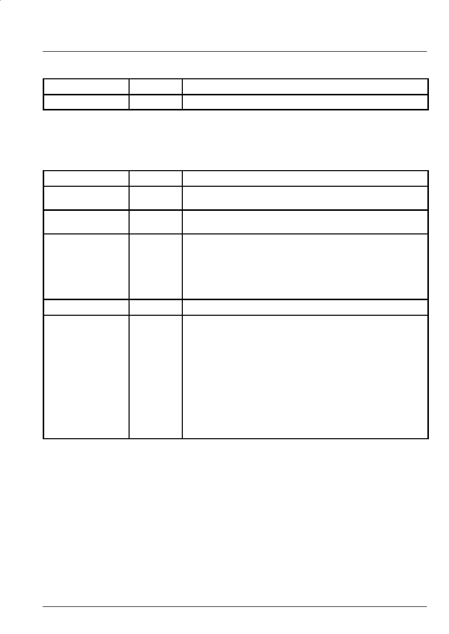
Table 8≠1: Data transfer between CCU and DMA 2275/2286
Addr.
No.
Bit
No.
Direct.
MSB
15
14
13
12
11
10
9
8
7
6
5
4
3
2
1
0
LSB
5
6
7
8
9
10
203
194
195
196
197
198
204
205
206
208
209
210
W
W
W
R/W
R
W
W
W
W
W
W
W
W
W
R
R
R
R
0
0
0
0
0
EXA
Extension Address
0
0
0
0
0
WRA
Write Address
0
0
0
0
0
RDA
Read Address
this is an 8 bit register
this is an 8 bit register
0
DAT
Data
0
0
0
0
0
EXD
Extension Data
BUS
Busy
RRQ
Read
Request
WRQ
Write
Request
0
TT15
0
TT14
0
TT13
0
TT12
0
TT11
0
TT10
0
TT9
0
TT8
0
TT7
0
TT6
0
TT5
0
TT4
0
TT3
0
TT2
0
TT1
0
TT0
S
C1M
Channel Mode
HQ
H
L
0
C1U
Mode
Update
0
C1E
Channel
Enable
0
C1A
Channel Packet Address
S
C2M
Channel Mode
HQ
H
L
0
C2U
Mode
Update
0
C2E
Channel
Enable
0
C2A
Channel Packet Address
S
C3M
Channel Mode
HQ
H
L
0
C3U
Mode
Update
1
C3E
Channel
Enable
82
C3A
Channel Packet Address
S
C4M
Channel Mode
HQ
H
L
0
C4U
Mode
Update
0
C4E
Channel
Enable
0
C4A
Channel Packet Address
106
SFS
Subframe Select
1
DRS
Data
Rate
Select
0
AUM
Auto
Mode
1
CD
Chip
Defin.
0
0
0
0
0
0
0
0
0
0
0
0
0
0
0
0
0
CS
Chip
Select
0
DSB
Disable
S Bus
0
P0C
P0
Clear
0
P0R
P0
Reset
0
DGT
Data Group Type
12
SBE
S Bus Enable
0
TT15
0
TT14
0
TT13
0
TT12
0
TT11
0
TT10
0
TT9
0
TT8
0
TT7
0
TT6
0
TT5
0
TT4
0
TT3
0
TT2
0
TT1
0
TT0
0
C3S
Status
0
C4S
0
P0S
0
C2S
0
C1S
0
0
0
BER
Bit Error Rate
S
C4L
Coding Law CH4
HQ
H
L
S
C3L
Coding Law CH3
HQ
H
L
S
C2L
Coding Law CH2
HQ
H
L
S
C1L
Coding Law CH1
HQ
H
L
PSH
Packet 0 Syndrom High Byte
PSL
Packet 0 Syndrom Low Byte
PDH
Packet 0 Data High Byte
PDL
Packet 0 Data Low Byte
Bit must be set to zero for write registers (W) and are
don't care for read registers (R)

DMA 2275, DMA 2286
15
Table 8≠2: IM Bus register of DMA 2275/2286
Address
Label
Bit No.
Function
5
EXA
0≠11
extension address
6
WRA
0≠11
write address
bit 10: test option 2
1 = write (EXA) into fp_ram, address = (WRA)
7
RDA
0≠11
read address
bit 10: test option 2
1 = read fp_ram into DAT and EXA, address = (RDA)
bit 11: test option 1
1 = causes fp_jump to (EXA)
8
DAT
0≠7
data (from dram or fp_ram)
9
WRQ
RRQ
BUS
EXD
0
1
2
3≠6
write request
read request
imbus busy
1 = imbus interface busy
extension data
4 msb of fp_data, but in reverse order
10
TT0
TT1
TT2
TT3
TT4
TT5
TT6
TT7
TT8
TT9
TT10
TT11
TT12
TT13
TT14
TT15
0
1
2
3
4
5
6
7
8
9
10
11
12
13
14
15
for test only
bypass line memory
for test only
for test only
for test only
for test only
gray decoder input 0 = 7 bit
1 = 8 bit
for test only
for test only
for test only
for test only
for test only
for test only
for test only
for test only
for test only

DMA 2275, DMA 2286
16
Table 8≠3: IM Bus register of the DMA 2286
Address
Label
Bit No.
Function
203
C1A
C1E
C1U
C1M
0≠9
10
11
12≠15
channel 1 packet address
channel 1 packet selection enable
channel 1 mode update
channel 1 mode
194
see register 203
channel 2
195
see register 203
channel 3
196
see register 203
channel 4
197
SFS
CD
AUM
DRS
0≠10
13
14
15
subframe select
SFS = sample number of the first bit in the selected subframe
examples:
DRS = 1,
first subframe
SFS = 7
DRS = 1,
second subframe SFS = 106
DRS = 0,
first subframe
SFS = 14
chip definition
0 = DMA 2271/2281
undelayed packet output of sound proc.
1 = DMA 2286
packet output delayed by 128
µ
s
auto mode
0 = auto mode off
1 = sound coding in packet header
data rate select
0 = 10.125 Mb/s
D2 MAC
1 = 20.25 Mb/s
C/D MAC
198
CS
14, 15
chip select
0 = imbus of DMA 2271/2281 active
1 = imbus of DMA 2286 active
204
SBE
DGT
P0R
P0C
DSB
0≠3
4≠7
8
9
10
s_bus enable, each bit enables one s_bus channel
data group type selection
packet 0 reset
1: select first byte in packet 0 buffer (first byte = data group type DGT)
packet 0 clear
1: enable packet 0 buffer to store next packet 0
disable s_bus data output (pin 66)
0 = enabled
1 = high impedance
linear/nicam
hamming/parity protection
high/medium quality
stereo/mono
channel 1 enable
channel 2 enable
channel 3 enable
channel 4 enable

DMA 2275, DMA 2286
17
Table 8≠3, continued
Address
Label
Bit No.
Function
205
T0
T1
T2
T3
T4
T5
T6
T7
T8
T9
T10
T11
T12
T13
T14
T15
0
1
2
3
4
5
6
7
8
9
10
11
12
13
14
15
for test only
for test only
for test only
for test only
for test only
for test only
enable packet descrambler
for test only
disable error concealment
for test only
for test only
for test only
for test only
for test only
for test only
for test only
206
BER
C1S
C2S
C3S
C4S
P0S
0≠7
10
11
12
13
14
bit error rate:
number of erroneous bits of 82 packet headers within one frame,
detected by the golay decoder
status of sound signal selected by C1A
0: sound signal is inactive or interrupted
1: sound signal is present
status of sound signal selected by C2A
0: sound signal is inactive or interrupted
1: sound signal is present
status of sound signal selected by C3A
0: sound signal is inactive or interrupted
1: sound signal is present
status of sound signal selected by C4A
0: sound signal is inactive or interrupted
1: sound signal is present
status of packet 0 buffer
0: packet 0 selected by DGT not received
1: packet 0 received
208
C1L
C2L
C3L
C4L
0≠3
4≠7
8≠11
12≠15
coding law of sound signal selected by C1A
coding law of sound signal selected by C2A
coding law of sound signal selected by C3A
coding law of sound signal selected by C4A
L =
0: companded law
1: linear law
H =
0: first level protection
1: second level protection
HQ = 0: medium quality sound
1: high quality sound
S =
0: monophonic sound
1: stereophonic sound

DMA 2275, DMA 2286
18
Table 8≠3, continued
Address
Label
Bit No.
Function
209
PSL
PSH
0≠7
8≠15
packet 0 syndrom low byte
packet 0 syndrom high byte
PSL + PSH = 0:
packet 0 received without error
PSL + PSH > 0:
packet 0 received with error
210
PDL
PDH
0≠7
8≠15
packet 0 data low byte
packet 0 data high byte
8.3. DRAM Interface
The data transfer between descrambler chip and acqui-
sition DRAM interface controlled by the FP. The external
64 k x 1 bit DRAM has to store the following data
streams:
≠ line 625
28 byte/40ms
5600 bit/s
≠ packet bus
2 x 96 byte/448
µ
s
3430000 bit/s
≠ IM bus
500000 bit/s
The 1 bit DRAM interface offers a maximum data rate of
5.0625 Mbit/s by using four 20.25 MHz cycles for one
page mode read or write access. A 150 ns DRAM fulfills
the access time requirements. Fig. 9≠14 shows the
DRAM interface waveform. Refresh of the DRAM is con-
trolled by the FP, which starts a number of refresh cycles
within every line. An 8 bit refresh is performed to allow
the use of 256 Kbit DRAMs.
The acquisition DRAM is used on one side to store re-
ceived packet data and line 625 information needed by
the CCU and the conditional access subsystem (CASS)
and on the other side to store control information needed
by the descrambler chip (e.g. control words, filter coeffi-
cients, packet addresses etc.). Therefore, the descram-
bler chip does not include special IM bus registers ex-
cept those for subaddressing and sound processing (on
the DMA 2286 only).
The upper end of the DRAM address space can be used
as a scratch buffer for the CCU software. This DRAM
area is also refreshed and will never be used by the des-
crambler chip.

DMA 2275, DMA 2286
19
8.4. DRAM Memory Map
8.4.1. Mode Register
Name
Address
Function
mode_register
0000
6*8 bit
access_mode
0000
8 bit
bit 0: video cond. access
(0 = free / 1 = conditional)
bit 1: data1 cond. access
(0 = free / 1 = conditional)
bit 2: data2 cond. access
(0 = free / 1 = conditional)
bit 3: data3 cond. access
(0 = free / 1 = conditional)
bit 4: data4 cond. access
(0 = free / 1 = conditional)
bit 5: not used
bit 6: not used
bit 7: not used
video_mode
0008
8 bit
bit 0: peaking select
(0 = low / 1 = high)
bit 1: peaking
(1 = on)
bit 2: baseband filter
(1 = on)
bit 3: interpol. filter
(1 = on)
bit 4: load coeff
(1 = now)
bit 5: black out
(1 = on)
bit 6: gray decoder
(1 = on)
bit 7: line delay
(1 = off)
scram_mode
0010
8 bit
bit 0: video descrambling
(0 = on)
bit 1: video rotation
(0 = double / 1 = single)
bit 2: aspect ratio
(0 = 4:3 / 1 = 16:9)
bit 3: vbi descrambling
(1 = on)
bit 4: coeff clock
(1 = on)
bit 5: not used
bit 6: not used
bit 7: user panning
(1 = on)
mac_mode
0018
8 bit
bit 3≠0:
clamp position
bit 4:
clamp bypass
(1 = on)
bit 5:
freq select
(0 = 50 Hz / 1 = 60 Hz)
bit 6:
decoder sync
(1 = locked)
bit 7:
mac select
(0 = d2 / 1 = d)
pan_vector
0020
8 bit
bit 7≠0:
user pan vector
(2's complement)
pan_output
0028
8 bit
bit 7≠0:
pan vector output
(2's complement)
Edition: June 12, 1992
6251≠330≠1E

DMA 2275, DMA 2286
20
Mode Register
0000H
0008H
0010H
0018H
0020H
0028H
Access_mode < 7≠0 >
Video_mode < 7≠0 >
Scram_mode < 7≠0 >
Mac_mode < 7≠0 >
Pan_vector < 7≠0 >
Pan_output < 7≠0 >
address
bit
7
6
4
3
2
1
0
5
8.4.2. Pac1 Register
Name
Address
Function
pac1_register
0100
12*8 bit
spa_reg
0100
4*2*8 bit
bit 9≠0:
packet address
sps_reg
0140
4*8 bit
bit 0:
packet descrambling (1 = on)
bit 2,1:
packet location
(01 = 1st subframe)
(10 = 2nd subframe)
(00 = both subframes)
(11 = both subframes)
bit 3:
packet remove
(1 = on)
bit 4:
automode
(1 = on)
SPA Register
0100H
0108H
0110H
0118H
0120H
0128H
SPA1 < 9, 8 >
SPA3 < 7≠0 >
address
bit
7
6
4
3
2
1
0
5
SPA4 < 7≠0 >
SPA2 < 7≠0 >
SPA1 < 7≠0 >
SPA2 < 9, 8 >
SPA3 < 9, 8 >
SPA4 < 9, 8 >
0130H
0138H
SPS Register
0140H
0148H
0150H
0158H
SPS1 < 4≠0 >
SPS2 < 4≠0 >
SPS3 < 4≠0 >
SPS4 < 4≠0 >
7
6
4
3
2
1
0
5
address
bit

DMA 2275, DMA 2286
21
8.4.3. Pac2 Register
Name
Address
Function
pac2_register
0160
72*8 bit
pab_reg
0160
8*2*8 bit
bit 9≠0:
packet address
bit 10,11: continuity index
pae_reg
01e0
8*5*8 bit
bit 35≠0: packet address extension
psc_reg
0320
8*2*8 bit
bit 0:
packet acquisition
(1 = 0)
bit 2,1:
packet location
(01 = 1st subframe)
(10 = 2nd subframe)
(00 = both subframes)
(11 = both subframes)
bit 3:
cont. index select
(1 = on)
bit 6≠4:
packet type select
(000 = ignore packet type)
(001 = select F8 or 00)
(010 = select C7 or 3F)
(110 = select F8)
(101 = select C7)
(100 = select 00)
(111 = select 3F)
bit 8,7:
packet protection
(00 = not protected)
(01 = 8 byte Hamming [8,4])
(10 = full Hamming [8,4])
(11 = Golay [24,12])
bit 11≠9: packet addr. extens.
(000 = ignore pack. extension)
(001 = select1lsb of CI)
(010 = select 4bit of TG)
(011 = select 7msb of CI)
(100 = select 8bit of CI)
(101 = select 12 bit of CCA)
(110 = select 24bit of SCA
(111 = select 36bit of UCA)
bit 13,12: packet link
(00 = no packet link)
(01 = link by PT)
(10 = link by CI)
(11 = not defined)
bit 14:
pae select
(0 = in every packet)
(1 = in sync packet only)

DMA 2275, DMA 2286
22
PAB Register
0160H
0168H
0170H
0178H
0180H≠01d8H
PAB1 < 11≠8 >
PAB2 < 11≠8 >
7
6
4
3
2
1
0
5
PAB1 < 7≠0 >
PAB2 < 7≠0 >
PAB3 ≠ PAB8
address
bit
PAE Register
01e0H
01e8H
01f0H
01f8H
0200H
0208H≠0228H
PAE1 < 7≠0 >
PAE1 < 15≠8 >
PAE1 < 23≠16 >
PAE1 < 35≠32 >
7
6
4
3
2
1
0
5
0230H≠0250H
0258H≠0278H
0280H≠02a0H
02a8H≠02c8H
02d0H≠02f0H
02f8H≠0318H
PAE1 < 31≠24 >
PAE2 < 35≠0 >
PAE4 < 35≠0 >
PAE5 < 35≠0 >
PAE6 < 35≠0 >
PAE7 < 35≠0 >
PAE8 < 35≠0 >
PAE3 < 35≠0 >
address
bit
PSC Register
0320H
0328H
0330H
0338H
0340H≠0398H
PSC1 < 14≠8 >
PSC2 < 14≠8 >
7
6
4
3
2
1
0
5
PSC1 < 7≠0 >
PSC2 < 7≠0 >
PSC3 ≠ PSC8
address
bit

DMA 2275, DMA 2286
23
8.4.4. Coeff Register
Name
Address
Function
coeff_register
0400
16*8 bit
a3_coeff
a2_coeff
a1_coeff
a0_coeff
b3_coeff
b2_coeff
b1_coeff
b0_coeff
c3_coeff
c2_coeff
c1_coeff
c0_coeff
d3_coeff
d2_coeff
d1_coeff
d0_coeff
0400
0408
0410
0418
0420
0428
0430
0438
0440
0448
0450
0458
0460
0468
0470
0478
bit 5≠0:
6 bit integer value
(5)
bit 5≠0:
6 bit integer value
(13)
bit 5≠0:
6 bit integer value
(0)
bit 5≠0:
6 bit integer value
(1)
bit 5≠0:
6 bit integer value
(38)
bit 5≠0:
6 bit integer value
(46)
bit 5≠0:
6 bit integer value
(0)
bit 5≠0:
6 bit integer value
(25)
bit 5≠0:
6 bit integer value
(38)
bit 5≠0:
6 bit integer value
(25)
bit 5≠0:
6 bit integer value
(0)
bit 5≠0:
6 bit integer value
(46)
bit 5≠0:
6 bit integer value
(5)
bit 5≠0:
6 bit integer value
(1)
bit 5≠0:
6 bit integer value
(0)
bit 5≠0:
6 bit integer value
(13)
Coeff Register
0400H
0408H
0410H
0418H
0420H
0428H
A3_coeff < 5≠0 >
A2_coeff < 5≠0 >
A1_coeff < 5≠0 >
A0_coeff < 5≠0 >
B3_coeff < 5≠0 >
B2_coeff < 5≠0 >
7
6
4
3
2
1
0
5
B1_coeff < 5≠0 >
B0_coeff < 5≠0 >
C3_coeff < 5≠0 >
C2_coeff < 5≠0 >
C1_coeff < 5≠0 >
C0_coeff < 5≠0 >
D3_coeff < 5≠0 >
D2_coeff < 5≠0 >
D1_coeff < 5≠0 >
D0_coeff < 5≠0 >
0430H
0438H
0440H
0448H
0450H
0458H
0460H
0468H
0470H
0478H
address
bit

DMA 2275, DMA 2286
24
8.4.5. CW Register
Name
Address
Function
cw_register
0600
96*8 bit
lcw_even
lcw_odd
vcw_even
vcw_odd
dcw1_even
dcw1_odd
dcw2_even
dcw2_odd
dcw3_even
dcw3_odd
dcw4_even
dcw4_odd
0600
0640
0680
06c0
0700
0740
0780
07c0
0800
0840
0880
08c0
8*8 bit local control word
8*8 bit local control word
8*8 bit video control word
8*8 bit video control word
8*8 bit data control word
8*8 bit data control word
8*8 bit data control word
8*8 bit data control word
8*8 bit data control word
8*8 bit data control word
8*8 bit data control word
8*8 bit data control word
0800H≠0838H
CW Register
0600H
0608H≠0630H
0638H
0640H
0648H≠0670H
0678H
LCW_even < 7≠0 >
LCW_even < 55≠8 >
LCW_even < 59≠56 >
LCW_odd < 55≠8 >
7
6
4
3
2
1
0
5
0680H
0688H≠06b0H
06b8H
06c0H
06c8H≠06f0H
06f8H
LCW_odd < 7≠0 >
LCW_odd < 59≠56 >
VCW_even < 55≠8 >
VCW_even < 59≠56 >
VCW_odd < 7≠0 >
DCW1_even < 59≠0 >
VCW_odd < 59≠56 >
VCW_even < 7≠0 >
DCW1_odd < 59≠0 >
DCW2_even < 59≠0 >
DCW2_odd < 59≠0 >
DCW3_even < 59≠0 >
DCW3_odd < 59≠0 >
DCW4_even < 59≠0 >
DCW4_odd < 59≠0 >
VCW_odd < 55≠8 >
0700H≠0738H
0740H≠0778H
0780H≠07b8H
07c0H≠07f8H
0840H≠0878H
0880H≠08b8H
08c0H≠08f8H
address
bit

DMA 2275, DMA 2286
25
8.4.6. Error Buffer
Name
Address
Function
error_buffer
0c00
8*16*8 bit
buf1_error
buf2_error
buf3_error
buf4_error
buf5_error
buf6_error
buf7_error
buf8_error
0c00
0c80
0d00
0d80
0e00
0e80
0f00
0f80
16*8 bit
16*8 bit
16*8 bit
16*8 bit
16*8 bit
16*8 bit
16*8 bit
16*8 bit
bit 5≠0:
error_num
bit 6:
crc error
(1 = error)
bit 7:
not defined
0c80H≠0cf8H
Error Buffer
0c00H
0c08H
0c10H
0c18H
0c20H
0c28H
Pack1_error < 7≠0 >
Pack2_error < 7≠0 >
Pack3_error < 7≠0 >
Pack5_error < 7≠0 >
7
6
4
3
2
1
0
5
0c30H
0c38H
0c40H
0c48H
0c50H
0c58H
Pack4_error < 7≠0 >
Pack6_error < 7≠0 >
Pack8_error < 7≠0 >
Pack9_error < 7≠0 >
Pack10_error < 7≠0 >
Pack13_error < 7≠0 >
Pack12_error < 7≠0 >
Pack7_error < 7≠0 >
Pack14_error < 7≠0 >
Pack15_error < 7≠0 >
Pack16_error < 7≠0 >
Buf2 Error
Buf3≠8 Error
Pack11_error < 7≠0 >
0c60H
0c68H
0c70H
0c78H
0d00H≠0fffH
address
bit

DMA 2275, DMA 2286
26
8.4.7. Packet Buffer
Name
Address
Function
packet_buf
1000
6144*8 bit
packet_buf1
packet_buf2
packet_buf3
packet_buf4
packet_buf5
packet_buf6
packet_buf7
packet_buf8
1000
2800
4000
5800
7000
8800
a000
b800
8*96*8 bit
8*96*8 bit
8*96*8 bit
8*96*8 bit
8*96*8 bit
8*96*8 bit
8*96*8 bit
8*96*8 bit
11b8H
48 Byte Packet Buffer
1000H
1008H
1010H
1018H
1020H
1028H
7
6
4
3
2
1
0
5
1030H
1038H
1040H≠1178H
1180H
1188H
1190H
1198H
11a0H
11a8H
11b0H
11c0H≠12f8H
1300H≠27f8H
PA < 7≠0 >
CI
Packet Type
Packet Data < 15≠8 >
Packet Data < 7≠0 >
Packet Data < 23≠16 >
Packet Data < 39≠32 >
Packet Data < 359≠40 >
Packet Type
Packet Data < 31≠24 >
CI
Packet 3≠16
PA < 9, 8 >
PA < 7≠0 >
PA < 9, 8 >
Packet Data < 15≠8 >
Packet Data < 7≠0 >
Packet Data < 23≠16 >
Packet Data < 39≠32 >
Packet Data < 359≠40 >
Packet Data < 31≠24 >
address
bit

DMA 2275, DMA 2286
27
1320H
96 Byte Packet Buffer
1000H
1008H
1010H
1018H
1020H
1028H
7
6
4
3
2
1
0
5
1030H
1038H
1040H≠12e0H
12e8H
12f0H
12f8H
1300H
1308H
1310H
1318H
1328H
1330H
PA < 7≠0 >
CI
Packet Type
Packet Data < 15≠8 >
Packet Data < 7≠0 >
Packet Data < 23≠16 >
Packet Data < 39≠32 >
Packet Data < 719≠40 >
Packet Data < 31≠24 >
CI
PA < 9, 8 >
PA < 9, 8 >
Packet Data < 7≠0 >
Packet Data < 23≠16 >
Packet Data < 39≠32 >
Packet Data < 719≠40 >
Packet Data < 31 ≠24 >
1338H
1340H≠15e0H
15e8H
15f0H
15f8H
1600H≠27f8H
Packet 3≠8
Packet Data < 15≠8 >
Packet Type
PA < 7≠0 >
address
bit

DMA 2275, DMA 2286
28
8.4.8. Line 625 Buffer
Name
Address
Function
line_625_buf
d000
28*8 bit
d080H
Line 625 Buffer
d000H
d008H
d010H
d018H
d020H
d028H
LINKS
UDT
CHID < 15≠8 >
7
6
4
3
2
1
0
5
d030H
d038H
d040H
d048H
d050H
d058H
CHID < 7≠0 >
SDFSCR
CAFCNT < 7≠0 >
CAFCNT < 15≠8 >
CAFCNT < 19≠16 >
BCH < 13≠8 >
BCH < 7≠0 >
MVSCG
SDF
FCNT
UDF
TDMCID
TDMS < 7≠0 >
Unallocated
d060H
d068H
d070H
d078H
d088H
d090H
d098H
d0a0H
d0a8H
d0b0H
d0b8H
d0c0H
d0c8H
d0d0H
d0d8H
TDMS < 15≠8 >
TDMS < 23≠16 >
TDMS < 47≠40 >
TDMS < 39≠32 >
TDMS < 55≠48 >
TDMS < 61≠56 >
TDM
BCH < 7≠0 >
BCH < 13≠8 >
TDMS < 31≠24 >
_Err
_Err
address
bit
DMA 2275, DMA 2286
29
8.4.9. Scratch Buffer
Name
Address
Function
scratch_buf
e000
1024*8 bit
8.5. FP Memory Map
Name
Address
Function
frame_count
line_count
019
020
12 bit
fcnt flywheel
12 bit
line counter
chroma_offset
luma_offset
033
034
12 bit
2's complement
12 bit
2's complement
pan_fifo
036
037
038
039
040
041
042
8 bit
2's complement
(fifo output)
8 bit
2's complement
8 bit
2's complement
8 bit
2's complement
8 bit
2's complement
8 bit
2's complement
8 bit
2's complement
(fifo input)
packet_count
091
12 bit
packet counter
buf1_status
buf2_status
buf3_status
buf4_status
buf5_status
buf6_status
buf7_status
buf8_status
248
249
250
251
252
253
254
255
12 bit
12 bit
12 bit
12 bit
12 bit
12 bit
12 bit
12 bit
bit 4≠0:
buffer pointer
bit 5:
buffer appl.
(0 = standard/1 = ring)
bit 6:
buffer inc.
(0 = 96 byte/1 = 48 byte)
bit 7:
buffer enable
(0 = close/1 = open)
bit 8:
link status
(1 = active)
bit 11≠9: not used

DMA 2275, DMA 2286
30
…………………………………………………
…………………………………………………
…………………………………………………
…………………………………………………
…………………………………………………
…………………………………………………
…………………………………………………
…………………………………………………
…………………………………………………
…………………………………………………
…………………………………………………
FP Memory
19
20
33
34
Frame_count
Line_count
Luma_offset
7
6
4
3
2
1
0
5
91
248
249
250
251
Chroma_offset
Buf1_status < 8≠0 >
Buf2_status < 8≠0 >
Buf5_status < 8≠0 >
Buf4_status < 8≠0 >
Packet_count
Buf6_status < 8≠0 >
Buf7_status < 8≠0 >
Buf8_status < 8≠0 >
Buf3_status < 8≠0 >
252
253
254
255
8
9
11
10
address
bit
…………………………………………………
…………………………………………………
…………………………………………………
36≠42
Pan_fifo
…………………………………………………
…………………………………………………
…………………………………………………
…………………………………………………

DMA 2275, DMA 2286
31
9. Specifications
9.1. Outline Dimensions
Fig. 9≠1: DMA 2275/2286 in 68≠pin PLCC package
Weight approx. 4.5 g,
Dimensions in mm
9.2. Pin Connections
Pin Nr.
Signal Name
DMA 2275
Signal Name
DMA 2286
I/O
Symbol
1
Leave Vacant
Sound RAM Data
Input/Output
SDIO
2
Leave Vacant
Sound RAM Address A0
Output
SA0
3
Leave Vacant
Sound RAM Address A1
Output
SA1
4
Leave Vacant
Sound RAM Address A2
Output
SA2
5
Leave Vacant
Sound RAM Address A3
Output
SA3
6
Leave Vacant
Sound RAM Address A4
Output
SA4
7
Leave Vacant
Sound RAM Read/Write
Output
SR/W
8
Leave Vacant
Sound RAM RAS
Output
SRAS
9
Leave Vacant
Sound RAM Address A5
Output
SA5
10
Leave Vacant
Sound RAM Address A6
Output
SA6
11
Leave Vacant
Sound RAM Address A7
Output
SA7
12
IM Bus Clock
Input
IMC
13
IM Bus Ident
Input
IMI
14
IM Bus Data
Input/Output
IMD
15
Reset
Input
RES
16
M Main Clock
Input
MCLK
17
Burst Sync
Input
BSYNC
18
Leave Vacant

DMA 2275, DMA 2286
32
Pin Connections, continued
Pin Nr.
Signal Name
DMA 2275
Signal Name
DMA 2286
I/O
Symbol
19
Burst Data
Input
BDAT
20
VBI Data
Output
VBIDAT
21
Corrected Packet Data
Output
CPDAT
22
Packet Data
Input
PDAT
23
Descrambled Packet Data
Output
DPDAT
24
Baseband B0
Output
BO0
25
Baseband B1
Output
BO1
26
Baseband B2
Output
BO2
27
Baseband B3
Output
BO3
28
Baseband B4
Output
BO4
29
Baseband B5
Output
BO5
30
Baseband B6
Output
BO6
31
Baseband B7
Output
BO7
32
Ground
Supply
GND
33
Ground
Test Output
GND
34
Ground
Test Output
GND
35
Ground
Test Input
GND
36
Ground
Test Input
GND
37
Leave Vacant
38
Supply Voltage, +5 V
Supply
VSUP
39
Baseband B7
Input
BI7
40
Baseband B6
Input
BI6
41
Baseband B5
Input
BI5
42
Baseband B4
Input
BI4
43
Baseband B3
Input
BI3
44
Baseband B2
Input
BI2
45
Baseband B1
Input
BI1
46
Baseband B0
Input
BI0
47
IM Bus Busy
Output
IMBUS
48
Ground
Test Input
GND
49
Acq. RAM CAS
Output
ACAS

DMA 2275, DMA 2286
33
Pin Connections, continued
Pin Nr.
Signal Name
DMA 2275
Signal Name
DMA 2286
I/O
Symbol
50
Acq. RAM Data
Output
ADIO
51
Acq. RAM Address A0
Output
AA0
52
Acq. RAM Address A1
Output
AA1
53
Acq. RAM Address A2
Output
AA2
54
Acq. RAM Address A3
Output
AA3
55
Acq. RAM Address A4
Output
AA4
56
Acq. RAM Read/Write
Output
AR/W
57
Acq. RAM RAS
Output
ARAS
58
Acq. RAM Address A5
Output
AA5
59
Acq. RAM Address A6
Output
AA6
60
Acq. RAM Address A7
Output
AA7
61
Ground
Supply
GND
62
Ground
Test Input
GND
63
Supply Voltage, +5 V
Supply
VSUP
64
Leave Vacant
S_Bus Ident
Input
SBI
65
Leave Vacant
Audio Clock
Input
ACLK
66
Leave Vacant
S_Bus Data
Output
SBD
67
Leave Vacant
68
Leave Vacant
Sound RAM CAS
Output
SCAS
Note: Symbols for pin numbers 1 to 11, 64 to 66 and 68 are valid only for DMA 2286.

DMA 2275, DMA 2286
34
9.3. Pin Configuration
Fig. 9≠2: DMA 2286 in 68≠pin PLCC package
7
8
9
10
11
12
13
14
15
16
17
29 30 31 32 33 34 35 36 37 38 39
18
19
20
21
22
23
24
25
26
27 28
6
5
4
3
2
1
44
43
42
41
40
68 67 66 65 64 63 62 61
45
46
47
48
49
50
51
52
53
54
55
56
57
58
59
60
SDIO
SA0
SA1
SA2
SA3
SA4
SA5
SA6
SA7
IMC
IMI
IMD
BSYNC
MCLK
BDAT
VBIDAT
CPDAT
PDAT
DPDAT
BO0
BO1
BO2
BO3
BO4
BO5
BO6
BO7
GND
GND
GND
GND
GND
VSUP
BI7
BI6
BI5
BI4
BI3
BI2
BI1
BI0
IMBUS
GND
ADIO
AA0
AA1
AA2
AA3
AA4
AA5
AA6
AA7
GND
SBD
SBI
SR/W
SRAS
RES
ACLK
VSUP
GND
SCAS
AR/W
ARAS
ACAS
DMA 2286
9.4. Pin Descriptions
Pin 1 ≠ Sound RAM Data Input/Output (Fig. 9≠8)
Pin 1 serves as output for writing sound data into the ex-
ternal sound RAM and as input for reading sound data
from that RAM.
Pins 2 to 6 and 9 to 11 ≠ Sound RAM Address A0 to A7
Output (Fig. 9≠11)
These pins are used for addressing the external sound
RAM.
Pin 7 ≠ Sound RAM Read/Write Output (Fig. 9≠11)
By means of this output the external sound RAM is
switched to the read or write mode as required.
Pin 8 ≠ Sound RAM Row Address Select Output (Fig.
9≠11)
This pin supplies the Row Address Select signal (RAS)
to the external sound RAM.
Pins 12, 13 and 14 ≠ IM Bus Connection (Figs. 9≠3 and
9≠7)
These pins connect the DMA 2275/2286 to the IM bus.
Via the IM bus the DMA 2275/2286 communicates with
the CCU Central Control Unit.
Pin 15 ≠ Reset Input (Fig. 9≠6)
Pin 15 is used for hardware reset. Reset is actuated at
Low level, and at High level the DAM 2275/2286 is ready
for operation.
Pin 16 ≠
M Main Clock Input (Fig. 9≠5)
By means of this input, the DMA 2275/2286 receives the
required main clock signal of 20.25 MHz form the MCU
2600 Clock Generator IC.
Pin 17 ≠ Burst Sync Input (Fig. 9≠3)
By means of this input, the DMA 2275/2286 receives the
required burst sync pulse from the DMA 2271/2281. This
sync pulse is used both as line sync and frame sync.
Pin 19 ≠ Burst Data Input (Fig. 9≠3)
By means of this input, the DMA 2275/2286 receives the
decoded burst data of each line from the DMA
2271/2281.
Pin 20 ≠ VBI Data Output (Fig. 9≠11)
This pin supplies the descrambled burst data of each
line. This signal may serve as an input signal for the TPU
2735 Teletext Processor.
Pin 21 ≠ Corrected Packet Data Output (Fig. 9≠11)
This pin supplies descrambled and error corrected pack-
ets from two subframes required by external teletext or
other data processors.
Pin 22 ≠ Packet Data Input (Fig. 9≠3)
Via this pin, the DMA 2275/2286 receives packets of
one subframe from pin 55 of the DMA 2271/2281. These
packets are already de≠interleaved, with golay≠cor-
rected header and error≠corrected PT byte.
Pin 23 ≠ Descrambled Packet Data Output (Fig. 9≠11)
This pin supplies descrambled sound packets from one
subframe to pin 56 of the DMA 2271/2281.
Pins 24 to 31 ≠ Baseband B0 to B7 Output (Fig. 9≠11)
Via these pins, the DMA 2275/2286 delivers the digital
baseband signal including the descrambled video signal
to the DMA 2271/2281, where it is decoded into luma,
chroma and sound signals.
Pins 32 to 26 and 48, 61 and 62 ≠ Ground
These pins must be connected to the negative (ground)
of the supply voltage.

DMA 2275, DMA 2286
35
Pins 38 and 63 ≠ Supply Voltage
These pins must be connected to the positive supply
voltage.
Pins 39 to 46 ≠ Baseband B7 to B0 Input (Fig. 9≠4)
Via these pins,the DMA 2275/2286 receives the digi-
tized baseband signal coming either from the VCU 2133
Video Codec in a 7≠bit parallel Gray code or from any
other A/D converter in 8≠bit parallel binary code.
Pin 47 ≠ IM Bus Busy Output (Fig. 9≠11)
This pin supplies a signal which indicates that the IM bus
interface of the DMA 2275/2286 is busy. As long as this
pin delivers a High level signal there should be no IM bus
transfer to or from the DMA 2275/2286.
Pin 49 ≠ Acq. RAM Column Address Select Output (Fig.
9≠10)
This pin supplies the Column Address select signal
(CAS) to the external acquisition RAM.
Pin 50 ≠ Acq. RAM Data Input/Output (Fig. 9≠8)
Pin 50 serves as output for writing data into the external
acquisition RAM and as input for reading data from that
RAM.
Pins 51 to 55 and 58 to 60 ≠ Acq. RAM Address A0 to A7
Output (Fig. 9≠10)
These pins are used for addressing the external acquisi-
tion RAM.
Pin 56 ≠ Acq. RAM Read/Write Output (Fig. 9≠10)
By means of this output the external acquisition RAM is
switched to the read or write mode as required.
Pin 57 ≠ Acq. RAM Row Address Select Output (Fig.
9≠10)
This pin supplies the Row Address Select signal (RAS)
to the external acquisition RAM.
Pin 64 ≠ S Bus Ident Input (Fig. 9≠3)
Via this input, the DMA 2286 receives the ident signal of
the serial 3≠line S bus from the DMA 2281.
Pin 65 ≠ Audio Clock Input (Fig. 9≠5)
By means of this input, the DMA 2286 receives the re-
quired audio clock signal of 18.432 MHz from the DMA
2281.
Pin 66 ≠ S Bus Data Output (Fig. 9≠9)
This pin supplies the digital sound signal to the AMU
2481 Audio Mixer and can be connected to the S Bus
Data output of the DMA 2281. Only one S Bus Data out-
put should be activated for one S Bus sound channel.
Pin 68 ≠ Sound RAM Column Address Select Output
(Fig. 9≠11)
This pin supplies the Column Address Select signal
(CAS) to the external sound RAM.
9.5. Pin Circuits
The following figures schematically show the circuitry at
the various pins. The integrated protection structures
are not shown. The letter "P" means P≠channel, the let-
ter "N" N≠channel.
P
N
V
SUP
GND
Fig. 9≠3:
Input Pins 12, 13, 17, 19,
22 and 64
P
P
N
N
V
SUP
GND
BIAS
Fig. 9≠4:
Input Pins 39 to 46
P
N
P
N
GND
V
SUP
Fig. 9≠5:
Input Pins16 and 65
N
P
P
P
N
N
V
SUP
GND
Fig. 9≠6:
Input Pin 15
P
N
N
V
SUP
Fig. 9≠7:
Input/Output Pin 14
GND

DMA 2275, DMA 2286
36
Fig. 9≠8:
Input/Output Pins
1 and 50
P
P
N
N
V
SUP
GND
V
SUP
GND
N
Fig. 9≠9:
Output Pin 66
P
N
V
SUP
GND
Fig. 9≠10:
Output Pins 49, 51 to 60
P
N
V
SUP
GND
Fig. 9≠11:
Output Pins 2 to 11, 20,
21, 23 to 31, 47 and 68
9.6. Electrical Characteristics
All voltages are referred to ground.
9.6.1. Absolute Maximum Ratings
Symbol
Parameter
Pin No.
Min.
Max.
Unit
T
A
Ambient Operating Temperature
≠
0
65
∞
C
T
S
Storage Temperature
≠
≠40
+125
∞
C
V
SUP
Supply Voltage
38, 63
≠
6
V
V
I
Input Voltage, all Inputs
≠
≠0.3 V
V
SUP
≠
V
O
Output Voltage, all Outputs
≠
≠0.3 V
V
SUP
≠
I
O
Output Current, all Outputs
≠
≠10
+10
mA

DMA 2275, DMA 2286
37
9.6.2. Recommended Operating Conditions
Symbol
Parameter
Pin No.
Min.
Typ.
Max.
Unit
T
A
Ambient Operating Temperature
≠
0
≠
65
∞
C
V
SUP
Supply Voltage
38, 63
4.75
5.0
5.25
V
V
IMIL
IM Bus Input Low Voltage
12 to 14
≠
≠
0.8
V
V
IMIH
IM Bus Input High Voltage
2.0
≠
≠
V
R
ext
External Pull≠Up Resistor
1.0
≠
≠
k
f
I
I IM Bus Clock Frequency
0.05
≠
1000
kHz
t
IM1
I Clock Input Delay Time
after IM Bus Ident Input
0
≠
≠
ns
t
IM2
I Clock Input Low Pulse Time
500
≠
≠
ns
t
IM3
I Clock Input High Pulse Time
500
≠
≠
ns
t
IM4
I Clock Input Setup Time
before Ident Input High
0
≠
≠
ns
t
IM5
I Clock Input Hold Time
after Ident Input High
250
≠
≠
ns
t
IM6
I Clock Input Setup Time
before Ident End≠Pulse Input
1.0
≠
≠
µ
s
t
IM7
IM Bus Data Input Delay Time
after
I Clock Input
0
≠
≠
ns
t
IM8
IM Bus Data Input Setup Time
before
I Clock Input
0
≠
≠
ns
t
IM9
IM Bus Data Input Hold Time
after
I Clock Input
0
≠
≠
ns
t
IM10
IM Bus Ident End≠Pulse Low Time
1.0
≠
≠
µ
s
V
REIL
Reset Input Low Voltage
15
≠
≠
0.8
V
V
REIH
Reset Input High Voltage
2.0
≠
≠
V
t
REIL
Reset Input Low Time
2
≠
≠
µ
s
V
MIDC
M Clock Input D.C. Voltage
16
1.5
≠
3.5
V
V
MIAC
M Clock Input A.C. Voltage (p≠p)
0.8
≠
2.5
V
t
MIH
t
MIL
M Clock Input
High/Low Ratio
0.9
1.0
1.1
≠
t
MIHL
M Clock Input
High/Low Transition Time
≠
≠
0.15
f
M
s
f
M
M Clock Input Frequency
≠
20.25
≠
MHz

DMA 2275, DMA 2286
38
Recommended Operating Conditions, continued
Symbol
Parameter
Pin No.
Min.
Typ.
Max.
Unit
V
BBIL
Burst Bus Input Low Voltage
17, 19
≠
≠
0.8
V
V
BBIH
Burst Bus Input High Voltage
2.0
≠
≠
V
V
PDIL
Packet Data Input Low Voltage
22
≠
≠
0.8
V
V
PDIH
Packet Data Input High Voltage
2.0
≠
≠
V
V
BIL
Baseband Input Low Voltage
39 to 46
≠
≠
2.2
V
V
BIH
Baseband Input High Voltage
2.8
≠
≠
V
t
BIS
Baseband Input Setup Time
before falling edge of MCLK
39 to 46,
16
15
≠
50
ns
t
BIH
Baseband Input Hold Time
after falling edge of MCLK
0
≠
≠
ns
V
SIIL
S Bus Ident Input Low Voltage
64
≠
≠
0.4
V
V
SIIH
S Bus Ident Input High Voltage
2.0
≠
≠
V
t
SIIL
S Bus Ident Input Low Time
150
≠
≠
ns
V
AIDC
A Clock Input D.C. Voltage
65
1.5
≠
3.5
V
V
AIAC
A Clock Input A.C. Voltage (p≠p)
0.8
≠
2.5
V
t
AH
t
AL
A Clock Input
High/Low Ratio
0.9
1.0
1.1
≠
t
A
A Clock Input
High/Low Transition Time
≠
≠
0.15
f
A
s
f
A
A Clock Input Frequency
≠
18.432
≠
MHz

DMA 2275, DMA 2286
39
9.6.3. Characteristics at T
A
= 0 to 65
∞
C, V
SUP
= 4.75 to 5.25 V, f
M
= 20.25 MHz
Symbol
Parameter
Pin No.
Min.
Typ.
Max.
Unit
Test Conditions
I
SUP
Supply Current
38, 63
≠
120
160
mA
V
IMDOL
IM Bus Data Output
Low Voltage
14
≠
≠
0.4
V
I
IMO
= 5 mA
I
IMDOH
IM Bus Data Output
High Current
≠
≠
10
µ
A
V
IMO
= 5 V
t
IM8
IM Bus Data Output Setup Time
before IM Bus Clock Input
14, 12
0
≠
500
ns
t
IM9
IM Bus Data Output Hold Time
after IM Bus Clock Input
0
≠
≠
ns
V
VDOL
VBI Data Output Low Voltage
20
≠
≠
0.4
V
I
L
= 1.6 mA
V
VDOH
VBI Data Output High Voltage
2.4
≠
≠
V
≠I
L
= 0.1 mA
t
VDOT
VBI Data Output Transition Time
≠
≠
10
ns
C
L
= 10 pF
t
VDOD
VBI Data Output Delay Time
after falling edge of MCLK
20, 16
≠
0
≠
ns
V
PDOL
Packet Data Output Low Voltage
21, 23
≠
≠
0.4
V
I
L
= 1.6 mA
V
PDOH
Packet Data Output High Voltage
2.4
≠
≠
V
≠I
L
= 0.1 mA
t
PDOT
Packet Data Output
Transition Time
≠
≠
10
ns
C
L
= 10 pF
t
PDOD
Packet Data Output Delay Time
after rising edge of MCLK
21, 23,
16
≠
0
≠
ns
V
BOL
Baseband Output Low Voltage
24 to 31
≠
≠
0.4
V
I
L
= 1.6 mA
V
BOH
Baseband Output High Voltage
2.4
≠
≠
V
I
L
= ≠0.1 mA
t
BOT
Baseband Output
Transition Time
≠
≠
10
ns
C
L
= 10 pF
t
BOD
Baseband Output Delay Time
after falling edge of MCLK
24 to
31, 16
≠
20
≠
ns
V
IBOL
IM Bus Busy Output Low Voltage
47
≠
≠
0.4
V
I
L
= 1.6 mA
V
IBOH
IM Bus Busy Output
High Voltage
2.4
≠
≠
V
≠I
L
= 0.1 mA
t
IBOT
IM Bus Busy Output
Transition Time
≠
≠
10
ns
C
L
= 10 pF
V
SDOL
S Bus Data Output Low Voltage
66
≠
≠
0.3
V
I
SO
= 8 mA
I
SDOH
S Bus Data Output High Current
≠
≠
10
µ
A
V
SO
= 5 V
t
SDOD
S Bus Data Output Delay Time
after falling edge of ACLK
66, 65
≠
20
≠
ns

DMA 2275, DMA 2286
40
9.6.4. Sound DRAM Interface Characteristics at T
A
= 0 to 65
∞
C, V
SUP
= 4.75 to 5.25 V, f
A
= 18.432 MHz
Symbol
Parameter
Pin No.
Min.
Typ.
Max.
Unit
Test Conditions
V
DIL
RAM Data Input Low Voltage
1
≠
≠
0.8
V
V
DIH
RAM Data Input High Voltage
2.0
≠
≠
V
V
DOL
RAM Data Output Low Voltage
≠
≠
0.4
V
I
DO
= 1.6 mA
V
DOH
RAM Data Output High Voltage
2.4
≠
≠
V
≠I
DO
= 0.1 mA
t
DT
RAM Data Output
Transition Time
3
≠
10
ns
C
L
= 10 pF
t
DIS
RAM Data Input Setup Time
before CAS Output High
1, 8, 68
0
≠
75
ns
t
DIH
RAM Data Input Hold Time
after CAS Output High
0
≠
33
ns
t
DHR
RAM Data Output Hold Time
after RAS Output Low
140
≠
≠
ns
t
DS
RAM Data Output Setup Time
before CAS Output Low
20
≠
≠
ns
t
DH
RAM Data Output Hold Time
after CAS Output Low
80
≠
≠
ns
V
AOL
RAM Address Output
Low Voltage
2 to 6,
9 to 11
≠
≠
0.4
V
I
AO
= 1.6 mA
V
AOH
RAM Address Output
High Voltage
2.4
≠
≠
V
≠I
AO
= 0.1 mA
t
AT
RAM Address Output
Transition Time
3
≠
10
ns
C
L
= 10 pF
t
RAH
Row Address Output Hold Time
after RAS Output Low
2 to 6,
9 to 11,
8 68
22
≠
≠
ns
t
ASR
Row Address Output Setup
Time before RAS Output Low
8, 68
30
≠
≠
ns
t
AR
Column Address Output Hold
Time after RAS Output Low
125
≠
≠
ns
t
CAH
Column Address Output Hold
Time after CAS Output Low
70
≠
≠
ns
t
ASC
Column Address Output Setup
Time before CAS Output Low
10
≠
≠
ns
V
RASOL
RAS Output Low Voltage
8
≠
≠
0.4
V
I
RASO
= 1.6 mA
V
RASOH
RAS Output High Voltage
2.4
≠
≠
V
≠I
RASO
= 0.1 mA
t
RAST
RAS Output Transition Time
3
≠
10
ns
C
L
= 10 pF
t
RAS
RAS Output Low Pulsewidth
125
≠
3000
ns
t
RP
RAS Output Precharge Time
130
≠
≠
ns

DMA 2275, DMA 2286
41
Sound DRAM Interface Characteristics, continued
Symbol
Parameter
Pin No.
Min.
Typ.
Max.
Unit
Test Conditions
V
CASOL
CAS Output Low Voltage
68
≠
≠
0.4
V
I
CASO
= 1.6 mA
V
CASOH
CAS Output High Voltage
2.4
≠
≠
V
≠I
CASO
= 0.1 mA
t
CAST
CAS Output Transition Time
3
≠
10
ns
C
L
= 10 pF
t
CP
CAS Output Precharge Time
70
≠
≠
ns
t
CAS
CAS Output Low Pulsewidth
95
≠
150
ns
t
PC
Page Mode Cycle Time
170
≠
≠
ns
t
RSH
RAS Output Hold Time after
CAS Output Low
8, 68
110
≠
≠
ns
t
RCD
CAS Output Delay Time after
RAS Output
45
≠
≠
ns
t
CSH
CAS Output Hold Time after
RAS Output Low
170
≠
≠
ns
t
CRP
CAS Output Precharge Time
before RAS Output Low
150
≠
≠
ns
V
WOL
WRITE Output Low Voltage
7
≠
≠
0.4
V
I
WO
= 1.6 mA
V
WOH
WRITE Output High Voltage
2.4
≠
≠
V
≠I
WO
= 0.1 mA
t
WT
WRITE Output Transition Time
3
≠
10
ns
C
L
= 10 pF
t
CWL
WRITE Output Low before CAS
Output High
7, 8, 68
180
≠
≠
ns
t
WCH
WRITE Output Hold Time
after CAS Output Low
80
≠
≠
ns
t
RCH
WRITE Output Hold Time
after CAS Output High
50
≠
≠
ns
t
RRH
WRITE Output Hold Time
after RAS Output High
20
≠
≠
ns

DMA 2275, DMA 2286
42
9.6.5. Acquisition DRAM Interface Characteristics at T
A
= 0 to 65
∞
C, V
SUP
= 4.75 to 5.25 V, f
M
= 20.25 MHz
Symbol
Parameter
Pin No.
Min.
Typ.
Max.
Unit
Test Conditions
V
DIL
RAM Data Input Low Voltage
50
≠
≠
0.8
V
V
DIH
RAM Data Input High Voltage
2.0
≠
≠
V
V
DOL
RAM Data Output Low Voltage
≠
≠
0.4
V
I
DO
= 1.6 mA
V
DOH
RAM Data Output High Voltage
2.4
≠
≠
V
≠I
DO
= 0.1 mA
t
DT
RAM Data Output
Transition Time
3
≠
10
ns
C
L
= 10 pF
t
DIS
RAM Data Input Setup Time
before CAS Output High
50, 49,
57
≠
≠
50
ns
t
DIH
RAM Data Input Hold Time
after CAS Output High
25
≠
45
ns
t
DHR
RAM Data Output Hold Time
after RAS Output Low
250
≠
≠
ns
t
DS
RAM Data Output Setup Time
before CAS Output Low
40
≠
≠
ns
t
DH
RAM Data Output Hold Time
after CAS Output Low
130
≠
≠
ns
V
AOL
RAM Address Output
Low Voltage
51 to 55,
58 to 60
≠
≠
0.4
V
I
AO
= 1.6 mA
V
AOH
RAM Address Output
High Voltage
2.4
≠
≠
V
≠I
AO
= 0.1 mA
t
AT
RAM Address Output
Transition Time
3
≠
10
ns
C
L
= 10 pF
t
RAH
Row Address Output Hold Time
after RAS Output Low
51 to 55,
58 to 60,
49 57
60
≠
≠
ns
t
ASR
Row Address Output Setup
Time before RAS Output Low
49, 57
100
≠
≠
ns
t
AR
Column Address Output Hold
Time after RAS Output Low
80
≠
≠
ns
t
CAH
Column Address Output Hold
Time after CAS Output Low
50
≠
≠
ns
t
ASC
Column Address Output Setup
Time before CAS Output Low
20
≠
≠
ns
V
RASOL
RAS Output Low Voltage
57
≠
≠
0.4
V
I
RASO
= 1.6 mA
V
RASOH
RAS Output High Voltage
2.4
≠
≠
V
≠I
RASO
= 0.1 mA
t
RAST
RAS Output Transition Time
3
≠
10
ns
C
L
= 10 pF
t
RAS
RAS Output Low Pulsewidth
≠
1600
≠
ns
t
RP
RAS Output Precharge Time
100
≠
≠
ns

DMA 2275, DMA 2286
43
Acquisition DRAM Interface Characteristics, continued
Symbol
Parameter
Pin No.
Min.
Typ.
Max.
Unit
Test Conditions
V
CASOL
CAS Output Low Voltage
49
≠
≠
0.4
V
I
CASO
= 1.6 mA
V
CASOH
CAS Output High Voltage
2.4
≠
≠
V
≠I
CASO
= 0.1 mA
t
CAST
CAS Output Transition Time
3
≠
10
ns
C
L
= 10 pF
t
CP
CAS Output Precharge Time
80
≠
≠
ns
t
CAS
CAS Output Low Pulsewidth
90
≠
110
ns
t
PC
Page Mode Cycle Time
200
≠
≠
ns
t
RSH
RAS Output Hold Time after
CAS Output Low
49, 57
75
≠
≠
ns
t
RCD
CAS Output Delay Time after
RAS Output
75
≠
≠
ns
t
CSH
CAS Output Hold Time after
RAS Output Low
170
≠
≠
ns
t
CRP
CAS Output Precharge Time
before RAS Output Low
200
≠
≠
ns
V
WOL
WRITE Output Low Voltage
56
≠
≠
0.4
V
I
WO
= 1.6 mA
V
WOH
WRITE Output High Voltage
2.4
≠
≠
V
≠I
WO
= 0.1 mA
t
WT
WRITE Output Transition Time
3
≠
10
ns
C
L
= 10 pF
t
CWL
WRITE Output Low before
CAS Output High
56, 49,
57
275
≠
≠
ns
t
WCH
WRITE Output Hold Time
after CAS Output Low
125
≠
≠
ns
t
RCH
WRITE Output Hold Time
after CAS Output High
20
≠
≠
ns
t
RRH
WRITE Output Hold Time
after RAS Output High
25
≠
≠
ns

DMA 2275, DMA 2286
44
H
L
H
L
H
L
Ident
Clock
Data
1
2
3
4
6
7
8
9
10
11
12
13
16
or 24
LSB
Address
MSB LSB
Data
MSB
A
B
C
Section A
Section B
Section C
H
L
Data
H
L
Clock
H
L
Ident
Address LSB
Address MSB
Data MSB
5
t
IM1
t
IM3
t
IM2
t
IM7
t
IM8
t
IM9
t
IM4
t
IM5
t
IM6
t
IM10
Fig. 9≠12: IM bus waveforms
9.6.6. Waveforms
H
L
H
L
H
L
S≠Ident
S≠Clock
S≠Data
16 Bit Sound 1
A
Section A
Section B
H
L
S≠Data
H
L
S≠Clock
H
L
S≠Ident
LSB of Sound 1
MSB of Sound 4
16 Bit Sound 2
16 Bit Sound 3
16 Bit Sound 4
64 Clock Cycles
B
t
S1
t
S2
t
S4
t
S5
t
S3
t
S6
Fig. 9≠13: S bus waveforms

DMA 2275, DMA 2286
45
t
CWL
t
AR
t
CSH
t
PC
t
RAS
t
WCH
t
RRH
t
RP
t
RCH
t
CRP
t
CP
t
CAS
t
RCD
t
ASR
t
RAH
t
ASC
t
CAH
t
DS
t
DH
t
DHR
t
DIS
t
DIH
t
RSH
ROW ADDR.
COLUMN ADDR. 0
COLUMN ADDRESS 1
COLUMN ADDRESS 14
ROW ADDR.
VALID DATA
VALID DATA
VALID DATA
VALID DATA
VALID DATA
VALID DATA
V
OH
V
OL
WE
V
OH
V
OL
RAS
V
OH
V
OL
CAS
V
OH
V
OL
DRAM
ADDR.
V
OH
V
OL
DOUT
V
OH
V
OL
DIN
Fig. 9≠14: DRAM waveform

DMA 2275, DMA 2286
46
10. References
1. Specification of the systems of the MAC/packet fami-
ly. EBU Technical Document 3258≠E, Oct. 1986.
2. Data Sheet
DMA 2271, DMA 2281
C/D/D2≠MAC Decoder
ITT Semiconductors

DMA 2275, DMA 2286
47

DMA 2275, DMA 2286
MICRONAS INTERMETALL
48
MICRONAS INTERMETALL GmbH
Hans-Bunte-Strasse 19
D-79108 Freiburg (Germany)
P.O. Box 840
D-79008 Freiburg (Germany)
Tel. +49-761-517-0
Fax +49-761-517-2174
E-mail: docservice@intermetall.de
Internet: http://www.intermetall.de
Printed in Germany
by Simon Druck GmbH & Co., Freiburg (5/92)
Order No. 6251-330-1E
All information and data contained in this data sheet are with-
out any commitment, are not to be considered as an offer for
conclusion of a contract nor shall they be construed as to
create any liability. Any new issue of this data sheet invalidates
previous issues. Product availability and delivery dates are ex-
clusively subject to our respective order confirmation form; the
same applies to orders based on development samples deliv-
ered. By this publication, MICRONAS INTERMETALL GmbH
does not assume responsibility for patent infringements or
other rights of third parties which may result from its use.
Reprinting is generally permitted, indicating the source. How-
ever, our prior consent must be obtained in all cases.