 | –≠–ª–µ–∫—Ç—Ä–æ–Ω–Ω—ã–π –∫–æ–º–ø–æ–Ω–µ–Ω—Ç: HAL56x | –°–∫–∞—á–∞—Ç—å:  PDF PDF  ZIP ZIP |
HAL556, HAL560,
HAL566
Two-Wire Hall Effect
Edition Aug. 3, 2000
6251-425-2DS
MICRONAS
MICRONAS
Sensor Family

HAL55x, HAL56x
2
Micronas
Contents
Page
Section
Title
3
1.
Introduction
3
1.1.
Features
3
1.2.
Family Overview
4
1.3.
Marking Code
4
1.4.
Operating Junction Temperature Range
4
1.5.
Hall Sensor Package Codes
4
1.6.
Solderability
5
2.
Functional Description
6
3.
Specifications
6
3.1.
Outline Dimensions
6
3.2.
Dimensions of Sensitive Area
6
3.3.
Positions of Sensitive Areas
7
3.4.
Absolute Maximum Ratings
7
3.5.
Recommended Operating Conditions
8
3.6.
Electrical Characteristics
9
3.7.
Magnetic Characteristics Overview
12
4.
Type Descriptions
12
4.1.
HAL 556
14
4.2.
HAL 560
16
4.3.
HAL 566
18
5.
Application Notes
18
5.1.
Application Circuit
18
5.2.
Extended Operating Conditions
18
5.3.
Start-up Behavior
19
5.4.
Ambient Temperature
19
5.5.
EMC and ESD
20
6.
Data Sheet History

HAL55x, HAL56x
3
Micronas
Two-Wire Hall Effect Sensor Family
in CMOS technology
Release Notes: Revision bars indicate significant
changes to the previous edition.
1. Introduction
This sensor family consists of different two-wire Hall
switches produced in CMOS technology. All sensors
change the current consumption depending on the ex-
ternal magnetic field and require only two wires between
sensor and evaluation circuit. The sensors of this family
differ in the magnetic switching behavior and switching
points.
The sensors include a temperature-compensated Hall
plate with active offset compensation, a comparator, and
a current source. The comparator compares the actual
magnetic flux through the Hall plate (Hall voltage) with
the fixed reference values (switching points). According-
ly, the current source is switched on (high current
consumption) or off (low current consumption).
The active offset compensation leads to constant mag-
netic characteristics in the full supply voltage and tem-
perature range. In addition, the magnetic parameters
are robust against mechanical stress effects.
The sensors are designed for industrial and automotive
applications and operate with supply voltages from 4 V
to 24 V in the junction temperature range from ≠40
∞
C up
to 170
∞
C. All sensors are available in the SMD-package
SOT-89B and in the leaded version TO-92UA.
1.1. Features:
≠ current output for two-wire applications
≠ junction temperature range from ≠40
∞
C up to 170
∞
C.
≠ operates from 4 V to 24 V supply voltage
≠ operates with static magnetic fields and dynamic mag-
netic fields up to 10 kHz
≠ switching offset compensation at typically 145 kHz
≠ overvoltage and reverse-voltage protection
≠ magnetic characteristics are robust against mechani-
cal stress effects
≠ constant magnetic switching points over a wide supply
voltage range
≠ the decrease of magnetic flux density caused by rising
temperature in the sensor system is compensated by
a built-in negative temperature coefficient of the mag-
netic characteristics
≠ ideal sensor for applications in extreme automotive
and industrial environments
≠ EMC corresponding to DIN 40839
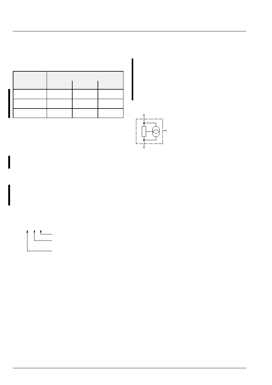
1.2. Family Overview
The types differ according to the mode of switching and
the magnetic switching points.
Type
Switching
Behavior
Sensitivity
see
Page
556
unipolar
very high
12
560
unipolar
inverted
low
14
566
unipolar
inverted
very high
16
Unipolar Switching Sensors:
The sensor turns to high current consumption with the
magnetic south pole on the branded side of the package
and turns to low consumption if the magnetic field is
removed. The sensor does not respond to the magnetic
north pole on the branded side.
Unipolar Inverted Switching Sensors:
The sensor turns to low current consumption with the
magnetic south pole on the branded side of the package
and turns to high consumption if the magnetic field is
removed. The sensor does not respond to the magnetic
north pole on the branded side.
HAL55x, HAL56x
4
Micronas
1.3. Marking Code
All Hall sensors have a marking on the package surface
(branded side). This marking includes the name of the
sensor and the temperature range.
Type
Temperature Range
A
K
E
HAL556
556A
556K
556E
HAL560
560A
560K
560E
HAL566
566A
566K
566E
1.4. Operating Junction Temperature Range
The Hall sensors from Micronas are specified to the chip
temperature (junction temperature T
J
).
A: T
J
= ≠40
∞
C to +170
∞
C
K: T
J
= ≠40
∞
C to +140
∞
C
E: T
J
= ≠40
∞
C to +100
∞
C
Note: Due to the high power dissipation at high current
consumption, there is a difference between the ambient
temperature (T
A
) and junction temperature. Please refer
section 5.4. on page 19 for details.
1.5. Hall Sensor Package Codes
Type: 556, 560, or 566
HAL XXXPA-T
Temperature Range: A, K, or E
Package: SF for SOT-89B
UA for TO-92UA
Type: 556
Package: TO-92UA
Temperature Range: T
J
= ≠40
∞
C to +100
∞
C
Example: HAL 556UA-E
Hall sensors are available in a wide variety of packaging
versions and quantities. For more detailed information,
please refer to the brochure: "Ordering Codes for Hall
Sensors".
1.6. Solderability
all packages: according to IEC68-2-58
During soldering reflow processing and manual rework-
ing, a component body temperature of 260
∞
C should not
be exceeded.
Components stored in the original packaging should
provide a shelf life of at least 12 months, starting from the
date code printed on the labels, even in environments as
extreme as 40
∞
C and 90% relative humidity.
Fig. 1≠1: Pin configuration
GND
2
1
V
DD
NC
3
HAL55x, HAL56x
5
Micronas
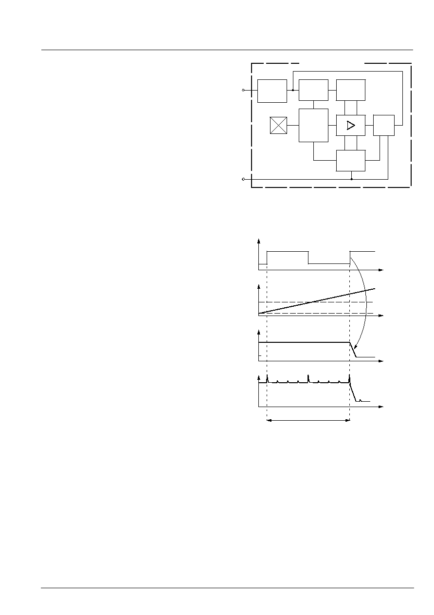
2. Functional Description
The HAL 55x, HAL 56x two-wire sensors are monolithic
integrated circuits which switch in response to magnetic
fields. If a magnetic field with flux lines perpendicular to
the sensitive area is applied to the sensor, the biased
Hall plate forces a Hall voltage proportional to this field.
The Hall voltage is compared with the actual threshold
level in the comparator. The temperature-dependent
bias increases the supply voltage of the Hall plates and
adjusts the switching points to the decreasing induction
of magnets at higher temperatures.
If the magnetic field exceeds the threshold levels, the
current source switches to the corresponding state. In
the low current consumption state, the current source is
switched off and the current consumption is caused only
by the current through the Hall sensor. In the high current
consumption state, the current source is switched on
and the current consumption is caused by the current
through the Hall sensor and the current source. The
built-in hysteresis eliminates oscillation and provides
switching behavior of the output signal without bounc-
ing.
Magnetic offset caused by mechanical stress is com-
pensated for by using the "switching offset compensa-
tion technique". An internal oscillator provides a two-
phase clock. In each phase, the current is forced through
the Hall plate in a different direction, and the Hall voltage
is measured. At the end of the two phases, the Hall volt-
ages are averaged and thereby the offset voltages are
eliminated. The average value is compared with the
fixed switching points. Subsequently, the current con-
sumption switches to the corresponding state. The
amount of time elapsed from crossing the magnetic
switching level to switching of the current level can vary
between zero and 1/f
osc
.
Shunt protection devices clamp voltage peaks at the
V
DD
-pin together with external series resistors. Reverse
current is limited at the V
DD
-pin by an internal series
resistor up to ≠15 V. No external protection diode is
needed for reverse voltages ranging from 0 V to ≠15 V.
Fig. 2≠1: HAL 55x, HAL 56x block diagram
Temperature
Dependent
Bias
Switch
Hysteresis
Control
Comparator
Current
Source
V
DD
1
Clock
Hall Plate
GND
2
HAL 55x, HAL 56x
Reverse
Voltage &
Overvoltage
Protection
t
I
DDlow
I
DD
1/f
osc
= 6.9
µ
s
I
DDhigh
B
B
OFF
f
osc
t
t
t
I
DD
t
B
ON
Fig. 2≠2: Timing diagram (example: HAL 56x)