
HAL621, HAL629
Hall Effect Sensor Family
6251-109-4E
Edition Feb. 5, 2001
6251-504-2DS
MICRONAS
MICRONAS
MICRONAS
MICRONAS
MICRONAS

HAL62x
2
Micronas
Contents
Page
Section
Title
3
1.
Introduction
3
1.1.
Features
3
1.2.
Family Overview
4
1.3.
Marking Code
4
1.3.1.
Special Marking of Prototype Parts
4
1.4.
Operating Junction Temperature Range
4
1.5.
Hall Sensor Package Codes
4
1.6.
Solderability
5
2.
Functional Description
6
3.
Specifications
6
3.1.
Outline Dimensions
6
3.2.
Dimensions of Sensitive Area
6
3.3.
Positions of Sensitive Areas
7
3.4.
Absolute Maximum Ratings
7
3.5.
Recommended Operating Conditions
8
3.6.
Electrical Characteristics
9
3.7.
Magnetic Characteristics Overview
12
4.
Type Descriptions
12
4.1.
HAL 621
14
4.2.
HAL 629
16
5.
Application Notes
16
5.1.
Ambient Temperature
16
5.2.
Start-up Behavior
16
5.3.
EMC
16
6.
Data Sheet History

HAL62x
3
Micronas
Hall Effect Sensor Family
in CMOS technology
Release Notes: Revision bars indicate significant
changes to the previous edition.
1. Introduction
The HAL 62x family consists of different Hall switches
produced in CMOS technology. All sensors include a
temperature-compensated Hall plate with active offset
compensation, a filter, a comparator, and an open-drain
output transistor. The comparator compares the actual
magnetic flux through the Hall plate (Hall voltage) with
the fixed reference values (switching points). According-
ly, the output transistor is switched on or off. The sensors
of this family differ in their magnetic characteristics.
All sensors contain an enhanced internal signal proces-
sing for very high repeatability requirements of the out-
put signal. These sensors are the optimal solution for
CAM and crank sensor applications.
The active offset compensation leads to magnetic pa-
rameters which are robust against mechanical stress ef-
fects. In addition, the magnetic characteristics are
constant in the full supply voltage and temperature
range.
The sensors are designed for industrial and automotive
applications and operate with supply voltages from
4.2 V to 24 V in the ambient temperature range from
≠40
∞
C up to 150
∞
C.
All sensors are available in the SMD-package (SOT-89B)
and in the leaded version (TO-92UA).
1.1. Features:
≠ switching offset compensation at typically 360 kHz
≠ signal processing with chopper stabilized filter
≠ operates from 4.2 V to 24 V supply voltage
≠ operates with static magnetic fields and dynamic mag-
netic fields up to 15 kHz
≠ overvoltage protection at all pins
≠ reverse-voltage protection at V
DD
-pin
≠ magnetic characteristics are robust against mechani-
cal stress effects
≠ short-circuit protected open-drain output by thermal
shut down
≠ constant switching points over a wide supply voltage
range
≠ ideal sensor for applications in extreme automotive
and industrial environments
≠ EMC and ESD optimized design
1.2. Family Overview
The types differ according to the magnetic flux density
values for the switching points and the mode of switch-
ing.
Type
Switching
Behavior
Sensitivity
see
Page
621
bipolar
very high
12
629
unipolar
medium
14
Note: The HAL 629 is the improved successor of the
HAL 628 with the same magnetic characteristics.
Bipolar Switching Sensors:
The output turns low with the magnetic south pole on the
branded side of the package and turns high with the
magnetic north pole on the branded side. The output
state is not defined for all sensors if the magnetic field is
removed again. Some sensors will change the output
state and some sensors will not.
Unipolar Switching Sensors:
The output turns low with the magnetic south pole on the
branded side of the package and turns high if the mag-
netic field is removed. The sensor does not respond to
the magnetic north pole on the branded side.

HAL62x
4
Micronas
1.3. Marking Code
All Hall sensors have a marking on the package surface
(branded side). This marking includes the name of the
sensor and the temperature range.
Type
Temperature Range
A
K
E
HAL 621
621A
621K
621E
HAL 629
629A
629K
629E
1.3.1. Special Marking of Prototype Parts
Prototype parts are coded with an underscore beneath
the temperature range letter on each IC. They may be
used for lab experiments and design-ins but are not in-
tended to be used for qualification tests or as production
parts.
1.4. Operating Junction Temperature Range
The Hall sensors from Micronas are specified to the chip
temperature (junction temperature T
J
).
A: T
J
= ≠40
∞
C to +170
∞
C
K: T
J
= ≠40
∞
C to +140
∞
C
E: T
J
= ≠40
∞
C to +100
∞
C
The relationship between ambient temperature (T
A
) and
junction temperature is explained in section 5.1. on page
16.
1.5. Hall Sensor Package Codes
Type: 62x
HAL XXXPA-T
Temperature Range: A, K, or E
Package: SF for SOT-89B
UA for TO-92UA
Type: 629
Package: TO-92UA
Temperature Range: T
J
= ≠40
∞
C to +100
∞
C
Example: HAL 629UA-E
Hall sensors are available in a wide variety of packaging
versions and quantities. For more detailed information,
please refer to the brochure: "Ordering Codes for Hall
Sensors".
1.6. Solderability
all packages: according to IEC68-2-58
During soldering reflow processing and manual rework-
ing, a component body temperature of 260
∞
C should not
be exceeded.
Components stored in the original packaging should
provide a shelf life of at least 12 months, starting from the
date code printed on the labels, even in environments as
extreme as 40
∞
C and 90% relative humidity.
OUT
GND
3
2
1
V
DD
Fig. 1≠1: Pin configuration
HAL62x
5
Micronas
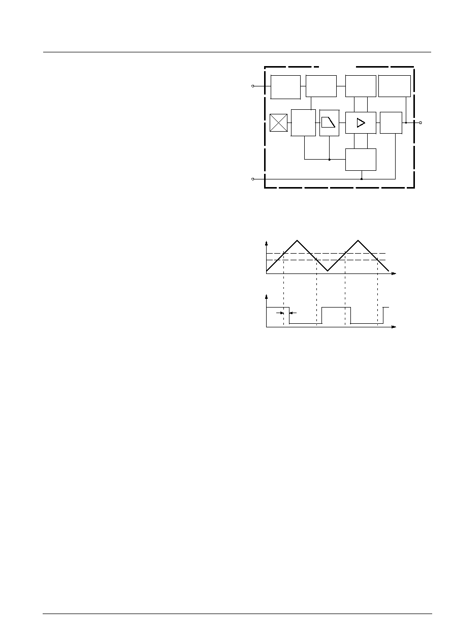
2. Functional Description
The HAL 62x sensors are monolithic integrated circuits
which switch in response to magnetic fields. If a magnet-
ic flux perpendicular to the sensitive area is applied to
the sensor, the Hall plate generates a Hall voltage pro-
portional to this field.
The total voltage which appears at the Hall plate is in-
fluenced by offset voltages (e. g. caused by mechanical
stress). This offset voltage is compensated for by cyclic
commutation of the connections for current flow and
voltage measurement which makes the switching offset
compensation technique possible. Therefore, an inter-
nal oscillator provides a clock. The output voltage of the
switched Hall plate contains the Hall voltage as a DC or
low frequency signal and the offset voltage as an AC sig-
nal at the chopper frequency. The following chopper sta-
bilized low-pass filter supresses the offset voltage and
the output signal is the offset compensated Hall voltage.
The following comparator block compares this offset
compensated Hall voltage with the defined switching
points. The output transistor is switched on when the
magnetic field becomes larger than the operating point
B
ON
. It remains in this state as long as the magnetic field
does not fall below the release point B
OFF
. If the magnet-
ic field falls below B
OFF
, the transistor is switched off until
the magnetic field once again exceeds B
ON
. The built-in
hysteresis eliminates oscillation.
According to the principle of the circuit, there is a fixed
delay time t
delay
of typical 25
m
s from crossing the mag-
netic thresholds to the switching of the output (see Fig.
2≠2).
The temperature-dependent bias regulates the supply
voltage of the Hall plates and adjusts the switching
points to the decreasing induction of magnets at higher
temperatures.
The output is short circuit protected by limiting high cur-
rents and by sensing overtemperature. Shunt protection
devices clamp voltage peaks at the Output-pin and V
DD
-
pin together with external series resistors. Reverse cur-
rent is limited at the V
DD
-pin by an internal series resistor
up to ≠15 V. No external reverse protection diode is
needed at the V
DD
-pin for reverse voltages ranging from
0 V to ≠15 V.
Temperature
Dependent
Bias
Switch
Hysteresis
Control
Comparator
Output
V
DD
1
OUT
3
Clock
Hall Plate
GND
2
HAL 62x
Fig. 2≠1: HAL 62x block diagram
Short Circuit &
Overvoltage
Protection
Reverse
Voltage &
Overvoltage
Protection
LP
Fig. 2≠2: Timing diagram
B
B
ON
V
O
t
t
B
OFF
t
delay

HAL62x
6
Micronas
3. Specifications
3.1. Outline Dimensions
Fig. 3≠1:
Plastic Small Outline Transistor Package
(SOT-89B)
Weight approximately 0.035 g
Dimensions in mm
4.55
1.7
min.
0.25
2.55
0.4
0.4
0.4
1.5
3.0
0.06
±
0.04
branded side
SPGS0022-5-A3/2E
y
1
2
3
4
±
0.2
0.15
0.3
2
0.2
sensitive area
top view
1.15
3.2. Dimensions of Sensitive Area
0.12 mm x 0.12 mm
3.3. Positions of Sensitive Areas
SOT-89B
TO-92UA
x
center of
the package
center of
the package
y
0.975 mm nominal
1.0 mm nominal
Fig. 3≠2:
Plastic Transistor Single Outline Package
(TO-92UA)
Weight approximately 0.12 g
Dimensions in mm
0.75
±
0.2
3.1
±
0.2
0.55
branded side
0.36
0.8
0.3
45
∞
y
14.0
min.
1.27
1.27
2.54
1
2
3
0.42
4.06
±
0.1
3.05
±
0.1
0.48
SPGS7002-9-A/2E
0.4
sensitive area
1.5
Note: For all package diagrams, a mechanical tolerance
of
±
0.05 mm applies to all dimensions where no tolerance
is explicitly given.
An improvement of the TO-92UA package with reduced
tolerances will be introduced end of 2001.

HAL62x
7
Micronas
3.4. Absolute Maximum Ratings
Symbol
Parameter
Pin No.
Min.
Max.
Unit
V
DD
Supply Voltage
1
≠15
28
1)
V
≠V
P
Test Voltage for Supply
1
≠24
2)
≠
V
≠I
DD
Reverse Supply Current
1
≠
50
1)
mA
I
DDZ
Supply Current through
Protection Device
1
≠200
3)
200
3)
mA
V
O
Output Voltage
3
≠0.3
28
1)
V
I
O
Continuous Output On Current
3
≠
50
1)
mA
I
Omax
Peak Output On Current
3
≠
250
3)
mA
I
OZ
Output Current through
Protection Device
3
≠200
3)
200
3)
mA
T
S
Storage Temperature Range
5)
≠65
150
∞
C
T
J
Junction Temperature Range
≠40
≠40
150
170
4)
∞
C
1)
as long as T
J
max
is not exceeded
2)
with a 220
series resistance at pin 1 (see Fig. 4≠9)
3)
t < 2 ms
4)
t < 1000h
5)
Components stored in the original packaging should provide a shelf life of at least 12 months, starting from the
date code printed on the labels, even in environments as extreme as 40
∞
C and 90% relative humidity.
Stresses beyond those listed in the "Absolute Maximum Ratings" may cause permanent damage to the device. This
is a stress rating only. Functional operation of the device at these or any other conditions beyond those indicated in the
"Recommended Operating Conditions/Characteristics" of this specification is not implied. Exposure to absolute maxi-
mum ratings conditions for extended periods may affect device reliability.
3.5. Recommended Operating Conditions
Symbol
Parameter
Pin No.
Min.
Max.
Unit
V
DD
Supply Voltage
1
4.2
24
V
I
O
Continuous Output On Current
3
0
20
mA
V
O
Output Voltage
(output switched off)
3
0
24
V

HAL62x
8
Micronas
3.6. Electrical Characteristics at T
J
= ≠40
∞
C to +170
∞
C , V
DD
= 4.2 V to 24 V, as not otherwise specified in Conditions
Typical Characteristics for T
J
= 25
∞
C and V
DD
= 12 V
Symbol
Parameter
Pin No.
Min.
Typ.
Max.
Unit
Conditions
I
DD
Supply Current
1
3.6
4.5
5.4
mA
T
J
= 25
∞
C
I
DD
Supply Current over
Temperature Range
1
2.2
4.5
7.2
mA
V
DDZ
Overvoltage Protection
at Supply
1
≠
28.5
32.5
V
I
DD
= 25 mA ,
T
J
= 25
∞
C,
t = 20 ms
V
OZ
Overvoltage Protection at Output
3
≠
28
32.5
V
I
OH
= 25 mA ,
T
J
= 25
∞
C,
t = 20 ms
V
OL
Output Voltage
3
≠
160
280
mV
I
OL
= 20 mA, T
J
= 25
∞
C
V
OL
Output Voltage over
Temperature Range
3
≠
160
400
mV
I
OL
= 20 mA
I
OH
Output Leakage Current
3
≠
0.01
0.1
µ
A
Output switched off,
T
J
= 25
∞
C, V
OH
24 V
I
OH
Output Leakage Current over
Temperature Range
3
≠
≠
10
µ
A
Output switched off,
T
J
150
∞
C, V
OH
24 V
f
osc
Internal Oscillator
Chopper Frequency
≠
≠
360
≠
kHz
T
J
= 25
∞
C
t
d
Delay Time between Switching
Threshold
D
B and Edge of Out-
put over Temperature Range
≠
≠
25
≠
µ
s
B > B
ON
+ 4 mT or
B < B
OFF
≠ 4 mT
t
en(O)
Enable Time of Output after
Setting of V
DD
3
≠
30
70
µ
s
V
DD
= 12 V
B > B
ON
+ 2 mT or
B < B
OFF
≠ 2 mT
t
r
Output Rise Time
3
≠
0.07
0.4
µ
s
V
DD
= 12 V, R
L
= 820 Ohm,
C
L
= 20 pF
t
f
Output Fall Time
3
≠
0.05
0.4
µ
s
V
DD
= 12 V, R
L
= 820 Ohm,
C
L
= 20 pF
R
thJSB
case
SOT-89B
Thermal Resistance Junction
to Substrate Backside
≠
≠
150
200
K/W
Fiberglass Substrate
30 mm x 10 mm x 1.5mm,
pad size see Fig. 3≠3
R
thJA
case
TO-92UA
Thermal Resistance Junction
to Soldering Point
≠
≠
150
200
K/W

HAL62x
9
Micronas
3.7. Magnetic Characteristics Overview at T
J
= ≠40
∞
C to +170
∞
C, V
DD
= 4.2 V to 24 V,
Typical Characteristics for V
DD
= 12 V
Magnetic flux density values of switching points.
Positive flux density values refer to the magnetic south pole at the branded side of the package.
Sensor
Parameter
On point B
ON
Off point B
OFF
Hysteresis B
HYS
Unit
Switching Type
T
J
Min.
Typ.
Max.
Min.
Typ.
Max.
Min.
Typ.
Max.
HAL 621
≠40
∞
C
≠1
1.2
4
≠3
≠0.7
2
1
1.9
3
mT
bipolar
25
∞
C
≠1
1.4
4
≠3
≠0.6
2
1
2
3
mT
170
∞
C
≠1
1.6
4
≠3
≠0.4
2
1
1.9
3
mT
HAL 629
≠40
∞
C
14.5
17.6
20.5
12.5
15.7
20
1
1.9
3
mT
unipolar
25
∞
C
14
17
20
12
15
19
1
2
3
mT
170
∞
C
11.5
15.6
19.2
10
13.7
17.2
1
1.9
3
mT
Note: For detailed descriptions of the individual types, see pages 12 and following.
Fig. 3≠3: Recommended pad size SOT-89B
Dimensions in mm
5.0
2.0
2.0
1.0

HAL62x
10
Micronas
≠15
≠10
≠5
0
5
10
15
20
≠15≠10 ≠5 0
5
10 15 20 25 30 35 V
mA
V
DD
I
DD
T
A
= ≠40
∞
C
T
A
= 25
∞
C
T
A
=100
∞
C
25
HAL 62x
Fig. 3≠4: Typical supply current
versus supply voltage
T
A
=170
∞
C
0
1
2
3
4
5
6
7
1
2
3
4
5
6
7 V
mA
V
DD
I
DD
HAL 62x
Fig. 3≠5: Typical supply current
versus supply voltage
T
A
= ≠40
∞
C
T
A
= 25
∞
C
T
A
=100
∞
C
T
A
=170
∞
C
0
1
2
3
4
5
6
7
≠50
0
50
100
150
200
∞
C
mA
T
A
I
DD
V
DD
= 4.2 V
V
DD
= 12 V
V
DD
= 24 V
HAL 62x
Fig. 3≠6: Typical supply current
versus ambient temperature
0
50
100
150
200
250
300
350
400
≠50
0
50
100
150
200
∞
C
mV
T
A
V
OL
HAL 62x
Fig. 3≠7: Typical output low voltage
versus ambient temperature
I
O
= 20 mA
V
DD
= 4.2 V
V
DD
= 12 V
V
DD
= 24 V

HAL62x
11
Micronas
0
50
100
150
200
250
300
350
400
0
5
10
15
20
25
30 V
mV
V
DD
V
OL
I
O
= 20 mA
HAL 62x
Fig. 3≠8: Typical output low voltage
versus supply voltage
T
A
= ≠40
∞
C
T
A
= 25
∞
C
T
A
=100
∞
C
T
A
=170
∞
C
0
50
100
150
200
250
300
350
400
3.5
4.0
4.5
5.0
5.5
6.0 V
mV
V
DD
V
OL
I
O
= 20 mA
HAL 62x
Fig. 3≠9: Typical output low voltage
versus supply voltage
T
A
= ≠40
∞
C
T
A
= 25
∞
C
T
A
=100
∞
C
T
A
=170
∞
C
15
20
25
30
35 V
m
A
V
OH
I
OH
T
A
= ≠40
∞
C
T
A
= 170
∞
C
T
A
= 150
∞
C
T
A
= 100
∞
C
T
A
= 25
∞
C
10
≠6
10
≠5
10
≠4
10
≠3
10
≠2
10
≠1
10
0
10
1
10
2
10
3
10
4
HAL 62x
Fig. 3≠10: Typical output leakage current
versus output voltage
≠50
0
50
100
150
200
∞
C
µ
A
T
A
I
OH
10
≠5
10
≠4
10
≠3
10
≠2
10
≠1
10
0
10
1
10
2
HAL 62x
Fig. 3≠11: Typical output leakage current
versus ambient temperature
V
O
= 24 V

HAL621
12
Micronas
4. Type Description
4.1. HAL 621
The HAL 621 is a very sensitive bipolar switching sensor
(see Fig. 4≠1).
The output turns low with the magnetic south pole on the
branded side of the package and turns high with the
magnetic north pole on the branded side. The output
state is not defined for all sensors if the magnetic field is
removed again. Some sensors will change the output
state and some sensors will not.
For correct functioning in the application, the sensor re-
quires both magnetic polarities (north and south) on the
branded side of the package.
Magnetic Features:
≠ switching type: bipolar
≠ very high sensitivity
≠ typical B
ON
: 1.4 mT at room temperature
≠ typical B
OFF
: ≠0.6 mT at room temperature
≠ operates with static magnetic fields and dynamic mag-
netic fields up to 15 kHz
Applications
The HAL 621 is the optimal sensor for all applications
with alternating magnetic signals and weak magnetic
amplitude at the sensor position such as:
≠ applications with large airgap or weak magnets,
≠ rotating speed measurement,
≠ crank shaft sensors,
≠ CAM shaft sensors, and
≠ magnetic encoders.
Fig. 4≠1: Definition of magnetic switching points for
the HAL 621
B
HYS
Output Voltage
0
B
OFF
B
ON
V
OL
V
O
B
Magnetic Characteristics at T
J
= ≠40
∞
C to +170
∞
C, V
DD
= 4.2 V to 24 V,
Typical Characteristics for V
DD
= 12 V
Magnetic flux density values of switching points.
Positive flux density values refer to the magnetic south pole at the branded side of the package.
Parameter
On point B
ON
Off point B
OFF
Hysteresis B
HYS
Magnetic Offset B
OFFSET
Unit
T
J
Min.
Typ.
Max.
Min.
Typ.
Max.
Min.
Typ.
Max.
Min.
Typ.
Max.
≠40
∞
C
≠1
1.2
4
≠3
≠0.7
2
1
1.9
3
0.2
mT
25
∞
C
≠1
1.4
4
≠3
≠0.6
2
1
2
3
0.4
mT
100
∞
C
≠1
1.4
4
≠3
≠0.5
2
1
1.9
3
0.4
mT
140
∞
C
≠1
1.5
4
≠3
≠0.4
2
1
1.9
3
0.5
mT
170
∞
C
≠1
1.6
4
≠3
≠0.4
2
1
1.9
3
0.6
mT
The hysteresis is the difference between the switching points B
HYS
= B
ON
≠ B
OFF
The magnetic offset is the mean value of the switching points B
OFFSET
= (B
ON
+ B
OFF
) / 2

HAL621
13
Micronas
≠3
≠2
≠1
0
1
2
3
0
5
10
15
20
25 V
mT
V
DD
B
ON
B
OFF
HAL 621
B
ON
B
OFF
Fig. 4≠2: Typ. magnetic switching points
versus supply voltage
T
A
= ≠40
∞
C
T
A
= 25
∞
C
T
A
= 100
∞
C
T
A
= 150
∞
C
≠3
≠2
≠1
0
1
2
3
3.5
4.0
4.5
5.0
5.5
6.0 V
mT
V
DD
B
ON
B
OFF
HAL 621
B
ON
B
OFF
Fig. 4≠3: Typ. magnetic switching points
versus supply voltage
T
A
= ≠40
∞
C
T
A
= 25
∞
C
T
A
= 100
∞
C
T
A
= 150
∞
C
≠3
≠2
≠1
0
1
2
3
≠50
0
50
100
150
200
∞
C
mT
T
A
B
ON
B
OFF
B
ON
B
OFF
HAL 621
Fig. 4≠4: Typ. magnetic switching points
versus temperature
V
DD
= 4.2 V
V
DD
= 12 V
V
DD
= 24 V

HAL629
14
Micronas
4.2. HAL 629
The HAL 629 is an unipolar switching sensor (see
Fig. 4≠5). The HAL 629 is the improved successor of the
HAL 628 with the same magnetic characteristics.
The output turns low with the magnetic south pole on the
branded side of the package and turns high if the mag-
netic field is removed. The sensor does not respond to
the magnetic north pole on the branded side.
For correct functioning in the application, the sensor re-
quires only the magnetic south pole on the branded side
of the package.
Magnetic Features:
≠ switching type: unipolar
≠ medium sensitivity
≠ typical B
ON
: 17 mT at room temperature
≠ typical B
OFF
: 15 mT at room temperature
≠ operates with static magnetic fields and dynamic mag-
netic fields up to 15 kHz
≠ typical temperature coefficient of magnetic switching
points is ≠600 ppm/K
Applications
The HAL 629 is the optimal sensor for applications with
one magnetic polarity such as:
≠ solid state switches,
≠ contactless solution to replace micro switches,
≠ position and end point detection, and
≠ rotating speed measurement.
B
HYS
Output Voltage
0
B
OFF
B
ON
V
OL
V
O
B
Fig. 4≠5: Definition of magnetic switching points for
the HAL 629
Magnetic Characteristics at T
J
= ≠40
∞
C to +170
∞
C, V
DD
= 4.2 V to 24 V,
Typical Characteristics for V
DD
= 12 V
Magnetic flux density values of switching points.
Positive flux density values refer to the magnetic south pole at the branded side of the package.
Parameter
On point B
ON
Off point B
OFF
Hysteresis B
HYS
Magnetic Offset
Unit
T
J
Min.
Typ.
Max.
Min.
Typ.
Max.
Min.
Typ.
Max.
Min.
Typ.
Max.
≠40
∞
C
14.5
17.6
20.5
12.5
15.7
20
1
1.9
3
16.6
mT
25
∞
C
14
17
20
12
15
19
1
2
3
16
mT
100
∞
C
12.7
16.3
19.6
11
14.4
18.1
1
1.9
3
15.4
mT
140
∞
C
12.1
15.9
19.4
10.4
14
17.6
1
1.9
3
15
mT
170
∞
C
11.5
15.6
19.2
10
13.7
17.2
1
1.9
3
14.6
mT
The hysteresis is the difference between the switching points B
HYS
= B
ON
≠ B
OFF
The magnetic offset is the mean value of the switching points B
OFFSET
= (B
ON
+ B
OFF
) / 2

HAL629
15
Micronas
0
5
10
15
20
0
5
10
15
20
25 V
mT
V
DD
B
ON
B
OFF
HAL 629
B
ON
B
OFF
Fig. 4≠6: Typ. magnetic switching points
versus supply voltage
T
A
= ≠40
∞
C
T
A
= 25
∞
C
T
A
= 100
∞
C
T
A
= 150
∞
C
0
5
10
15
20
3.5
4.0
4.5
5.0
5.5
6.0 V
mT
V
DD
B
ON
B
OFF
HAL 629
B
ON
B
OFF
Fig. 4≠7: Typ. magnetic switching points
versus supply voltage
T
A
= ≠40
∞
C
T
A
= 25
∞
C
T
A
= 100
∞
C
T
A
= 150
∞
C
0
5
10
15
20
≠50
0
50
100
150
200
∞
C
mT
T
A
B
ON
B
OFF
B
ON
B
OFF
HAL 629
Fig. 4≠8: Typ. magnetic switching points
versus temperature
V
DD
= 4.2 V
V
DD
= 12 V
V
DD
= 24 V

HAL62x
16
Micronas
5. Application Notes
5.1. Ambient Temperature
Due to the internal power dissipation, the temperature
on the silicon chip (junction temperature T
J
) is higher
than the temperature outside the package (ambient tem-
perature T
A
).
T
J
= T
A
+
T
At static conditions, the following equation is valid:
T = I
DD
* V
DD
* R
th
For typical values, use the typical parameters. For worst
case calculation, use the max. parameters for I
DD
and
R
th
, and the max. value for V
DD
from the application.
For all sensors, the junction temperature range T
J
is
specified. The maximum ambient temperature T
Amax
can be calculated as:
T
Amax
= T
Jmax
≠
T
5.2. Start-up Behavior
Due to the active offset compensation, the sensors have
an initialization time (enable time t
en(O)
) after applying
the supply voltage. The parameter t
en(O)
is specified in
the Electrical Characteristics (see page 8).
During the initialization time, the output state is not de-
fined and the output can toggle. After t
en(O)
, the output
will be low if the applied magnetic field B is above B
ON
.
The output will be high if B is below B
OFF
.
For magnetic fields between B
OFF
and B
ON
, the output
state of the HAL sensor after applying V
DD
will be either
low or high. In order to achieve a well-defined output
state, the applied magnetic field must be above B
ONmax
,
respectively, below B
OFFmin
.
Micronas GmbH
Hans-Bunte-Strasse 19
D-79108 Freiburg (Germany)
P.O. Box 840
D-79008 Freiburg (Germany)
Tel. +49-761-517-0
Fax +49-761-517-2174
E-mail: docservice@micronas.com
Internet: www.micronas.com
Printed in Germany
by Systemdruck+Verlags-GmbH, Freiburg (02/2001)
Order No. 6251-504-2DS
5.3. EMC and ESD
For applications with disturbances on the supply line or
radiated disturbances, a series resistor and a capacitor
are recommended (see figure 4≠9). The series resistor
and the capacitor should be placed as closely as pos-
sible to the sensor.
Applications with this arrangement passed the EMC
tests according to the product standards DIN 40839.
Note: The international standard ISO 7637 is similar to
the used product standard DIN 40839.
Please contact Micronas for the detailed investigation
reports with the EMC and ESD results.
OUT
GND
3
2
1
V
DD
4.7 nF
V
EMC
V
P
R
V
220
R
L
1.2 k
20 pF
Fig. 4≠9: Test circuit for EMC investigations
6. Data Sheet History
1. Final data sheet: "HAL 621, HAL 629, Hall Effect
Sensor Family", Feb. 3, 2000, 6251-504-1DS.
First release of the final data sheet.
2. Final data sheet: "HAL 621, HAL 629, Hall Effect
Sensor Family", Feb. 5, 2001, 6251-504-2DS.
Second release of the final data sheet. Major
changes:
≠ position of sensitive area in SOT-89B package
changed
All information and data contained in this data sheet are without any
commitment, are not to be considered as an offer for conclusion of a
contract, nor shall they be construed as to create any liability. Any new
issue of this data sheet invalidates previous issues. Product availability
and delivery are exclusively subject to our respective order confirma-
tion form; the same applies to orders based on development samples
delivered. By this publication, Micronas GmbH does not assume re-
sponsibility for patent infringements or other rights of third parties
which may result from its use.
Further, Micronas GmbH reserves the right to revise this publication
and to make changes to its content, at any time, without obligation to
notify any person or entity of such revisions or changes.
No part of this publication may be reproduced, photocopied, stored on
a retrieval system, or transmitted without the express written consent
of Micronas GmbH.