 | –≠–ª–µ–∫—Ç—Ä–æ–Ω–Ω—ã–π –∫–æ–º–ø–æ–Ω–µ–Ω—Ç: MAS3504D | –°–∫–∞—á–∞—Ç—å:  PDF PDF  ZIP ZIP |
MAS 3504D
G.729 Annex A
Edition Nov. 7, 2001
6251-522-1DS
MICRONAS
MICRONAS
MICRONAS
MICRONAS
MICRONAS
Voice Codec

MAS 3504D
2
Micronas
Contents
Page
Section
Title
4
1.
Introduction
4
1.1.
Features
5
1.2.
Application Overview
5
1.2.1.
Decoder Mode
5
1.2.2.
Encoder Mode
6
2.
Functional Description of the MAS 3504D
6
2.1.
DSP Core
6
2.2.
Firmware (Internal Program ROM)
6
2.2.1.
G.729 Encoder
6
2.2.2.
G.729 Decoder
6
2.3.
Program Download Feature
6
2.4.
Clock Management
6
2.5.
Power Supply Concept
6
2.5.1.
Internal Voltage Monitor
7
2.5.2.
DC/DC Converter
7
2.5.3.
Stand-by Functions
8
2.5.4.
Start-up Sequence
8
2.6.
Interfaces
8
2.6.1.
Parallel Input Output Interface (PIO)
8
2.6.2.
Parallel Data Output
9
2.6.3.
Parallel Data Input
9
2.6.3.1.
DMA Handshake Protocol
10
2.6.3.2.
End of DMA Transfer
10
2.6.4.
Audio Input Interface (SDI)
10
2.6.5.
Audio Output Interface (SDO)
11
2.6.5.1.
Example 1:16 Bits/Sample (I
2
S Compatible Data Format)
11
2.6.5.2.
Example 2:32 Bit/Sample (Inverted SOI)
12
3.
Control Interfaces
12
3.1.
I
2
C Bus Interface
12
3.1.1.
Device address and Subaddresses
13
3.2.
Command Structure
13
3.2.1.
Conventions for the Command Description
14
3.3.
Detailed MAS 3504D Command Syntax
14
3.3.1.
Run
14
3.3.2.
Write Register
14
3.3.3.
Write D0 Memory
14
3.3.4.
Write D1 Memory
15
3.3.5.
Read Register
15
3.3.6.
Read D0 Memory
15
3.3.7.
Read D1 Memory
16
3.4.
Version Number
16
3.5.
Register Table
16
3.5.1.
DC/DC Converter (Reg. 8E
hex
)
16
3.5.2.
User Control (Reg. FD
hex
)
17
3.5.2.1.
Data Transmission Format

Contents, continued
Page
Section
Title
MAS 3504D
Micronas
3
17
3.5.2.2.
Encoder Operation
17
3.5.2.3.
Decoder Operation
18
3.5.2.4.
Pause and Mute
18
3.5.3.
Volume Control (Reg. FC
hex
)
18
3.5.4.
Interface Control
18
3.5.4.1.
Wordlength Control (Reg. 74
hex
)
18
3.5.4.2.
Input Configuration (Reg. 61
hex
)
18
3.5.4.3.
Output Configuration (Reg. E1
hex
)
18
3.5.5.
Hardware Control (Reg. FA
hex
)
22
4.
Specifications
22
4.1.
Outline Dimensions
23
4.2.
Pin Connections and Short Descriptions
25
4.2.1.
Pin Descriptions
25
4.2.1.1.
Power Supply Pins
25
4.2.1.2.
DC/DC Converter Pins
25
4.2.1.3.
Control Lines
25
4.2.1.4.
Parallel Interface Lines
25
4.2.1.4.1.
PIO Handshake Lines
25
4.2.1.4.2.
PIO Data Lines
26
4.2.1.5.
Voltage Supervision And Other Functions
26
4.2.1.6.
Serial Input Interface
26
4.2.1.7.
Serial Output Interface
26
4.2.1.8.
Miscellaneous
26
4.2.2.
Pin Configurations
27
4.2.3.
Internal Pin Circuits
28
4.2.4.
Electrical Characteristics
28
4.2.4.1.
Absolute Maximum Ratings
29
4.2.4.2.
Recommended Operating Conditions
30
4.2.4.3.
Characteristics
31
4.2.4.3.1.
I
2
C Characteristics
32
4.2.4.3.2.
I
2
S Bus Characteristics ≠ SDI
33
4.2.4.3.3.
I
2
S Characteristics ≠ SDO
34
4.2.4.4.
DC/DC Converter Characteristics
36
4.2.4.5.
Typical Performance Characteristics
40
5.
Data Sheet History
License Notice
Supply of this implementation of G.729A technology does not convey a license nor imply any right to use this imple-
mentation in any finished end-user or ready-to-use final product. An independant license for such use is required.
For information on such license agreement please contact:
Sipro Lab Telecom Inc.
email: patriciam@sipro.com
http://www.sipro.com
Fax: +1 (514) 737-2327
MAS 3504D
4
Micronas
G.729 Annex A Voice Codec
1. Introduction
The MAS 3504D is a single-chip codec for use in
memory-based voice recording and playback applica-
tions. Due to embedded memories, the embedded DC/
DC up-converter, and the very low power consump-
tion, the MAS 3504D is ideally suited for portable elec-
tronics.
The MAS 3504D implements a voice encoder and
decoder that is compliant to the ITU Standard G.729
Annex A. This standard works on 8 kHz, 16 bit, mono
audio data that is compressed to 1 bit per audio sam-
ple. One second of compressed audio data uses
1000 bytes of memory.
1.1. Features
≠ Single-chip G.729 decoder
≠ G.729 Annex A encoder
≠ ITU compliance tests passed
≠ Parallel input and parallel output of coded bitstream
data
≠ Input audio data read from an I
2
S bus (in various
formats)
≠ Output audio data delivered via an I
2
S bus (in vari-
ous formats)
≠ Digital volume / mute
≠ Low power dissipation (150 mW for encoder,
80 mW for decoder @ 3.3 V)
≠ Supply voltage range: 1.0 V to 3.6 V due to built-in
DC/DC converter (1-cell battery operation)
≠ Adjustable power supply supervision
≠ Power-off function
≠ Additional functionality achievable via download
software (ADPCM encoder/decoder)
Fig. 1≠1: MAS 3504D block diagram
CLKI
decoded output
voice audio data
/3/
/3/
Serial In
I
2
C
RISC DSP Core
PIO
/3/
/8+5/
/2/
serial control
MAS 3504D
parallel I/O
DC/DC
Converter
Clock
Synthesizer
Serial Out
I
2
S
MAS 3504D
Micronas
5
1.2. Application Overview
The MAS 3504D can be applied in two major environ-
ments: as standalone decoder or as encoder/decoder
combination. For decoding only mode, the DAC 3550A
fits perfectly to the requirements of the MAS 3504D. It
is a high-quality multi sample rate DAC (8 kHz..
50 kHz) with internal crystal oscillator, which is only
needed for generating the decoder Clock, and inte-
grated stereo headphone amplifier plus two stereo
inputs.
1.2.1. Decoder Mode
In a memory-based voice playback environment, the
decoding is started with a command from a controller.
Then the MAS 3504D continuously requests frames of
G.729 data every 10 ms via the parallel (PIO) inter-
face.
A delayed response of the host to the request signal
(max. 20 milliseconds) will be tolerated by the
MAS 3504D as long as the input buffer does not run
empty. A PC might use its DMA capabilities to transfer
the data in the background to the MAS 3504D without
interfering with its foreground processes.
The source of the bit stream may be a memory (e.g.
ROM, Flash) or PC peripherals, such as CD-ROM
drive, a hard disk or a floppy disk drive.
1.2.2. Encoder Mode
For encoding a support routine must be downloaded to
the MAS 3504D via I
2
C. After the encoder is started, it
begins to encode the incoming audio data and writes
the coded datastream to the parallel (PIO) interface.
A delayed response of the host to the data available
signal (max. 20 milliseconds) will be tolerated by the
MAS 3504D as long as the output buffer does not
overrun.
Fig. 1≠2: Block diagram of a MAS 3504D, decoding a stored bit stream in a decoding only application
Fig. 1≠3: Block diagram of a MAS 3504D in an encoding/decoding application
ROM, CD-ROM,
RAM, Flash Mem. ..
Host
(PC, Controller)
I
2
S
line out
I
2
C
demand signal
demand clock
G.729 bit stream
CLKI
CLKOUT
18.432 MHz
MAS 3504D
DAC
3550A
ROM, CD-ROM,
RAM, Flash Mem. ..
Host
(PC, Controller)
clock
line in
I
2
C
CLKI
G.729 bit stream
Mic in
Handshake signals
line out
strobe
data out
data in
I
2
S lines
MAS 3504D
PLL
AD/DA

MAS 3504D
6
Micronas
2. Functional Description
2.1. DSP Core
The hardware of the MAS 3504D consists of a high
performance Digital Signal Processor and appropriate
interfaces. The processor works with a memory word
length of 20 bits and an extended range of 32 bits in its
accumulators. The instruction set of the DSP is highly
optimized for audio data compression and decompres-
sion. Thus, only very small areas of internal RAM and
ROM are required. All data input and output actions
are based on a `non cycle stealing' background DMA
that does not cause any computational overhead.
2.2. Firmware (Internal Program ROM)
The firmware fully contains a G.729 voice decoder.
With an additional support routine the IC is extended to
a G.729 Annex A encoder.
The G.729 standard compresses 8 kHz/16 bit mono
voice data in frames of 80 samples to 10 bytes each,
what results in a compressed bitstream of 1 bit/sam-
ple. The encoding according to Annex A has reduced
complexity, but is fully compatible to the initial G.729
standard. Therefore the MAS 3504D can decode bit-
streams that were encoded by other G.729 encoders
and it can encode bitstreams that can be decoded with
other G.729 decoders.
2.2.1. G.729 Encoder
For encoding operation the MAS 3504D has to be pre-
pared by downloading an additional routine to support
the encoder. After starting the encoder, 80 audio sam-
ples are continuously read via the serial input inter-
face. Each audio block of 80 samples is encoded to a
G.729 data frame consisting of 10 bytes which is sent
via the parallel interface. It is possible to monitor the
input audio samples also directly via the serial output
interface.
2.2.2. G.729 Decoder
The MAS 3504D expects a sequence of valid G.729
frames (10 bytes each) as input. The compressed data
is sent via the parallel interface. Each frame is
decoded to 80 audio samples, modified by the volume/
mute control and sent out via the serial output inter-
face.
2.3. Program Download Feature
The overall function of the MAS 3504D can be altered
by downloading up to 1 kWord program code into the
internal RAM and by executing this code instead of the
ROM code. During this time, G.729 processing is not
possible.
The code must be downloaded by the `write to mem-
ory' command (see Section 3.3. on page 14) into an
area of internal RAM. A `run' command starts the oper-
ation.
Micronas provides modules for encoding and decoding
audio data with ADPCM.
Detailed information about downloading is provided in
combination with the MAS 3504D software develop-
ment package from Micronas.
2.4. Clock Management
The MAS 3504D should be driven by a single clock at
a frequency of 18.432 MHz.
The CLKI signal acts as a reference for the embedded
clock synthesizer that generates the internal system
clock.
2.5. Power Supply Concept
The MAS 3504D offers an embedded controlled DC/
DC converter and voltage monitoring circuits for bat-
tery based power supply concepts. It works as an up-
converter. The application circuit for the DC/DC con-
verter is shown in Fig. 2≠1.
2.5.1. Internal Voltage Monitor
An internal voltage monitor compares the input voltage
at the VSENS pin with an internal reference value that
is adjustable via I
2
C bus. The PUP output pin becomes
inactive when the voltage at the VSENS pin drops
below the programmed value of the reference voltage.
It is important that the WSEN must not be activated
before the PUP is generated. The PUP signal thresh-
olds are listed in Table 3≠8 on page 19.
MAS 3504D
Micronas
7
2.5.2. DC/DC Converter
The DC/DC converter of the MAS 3504D is used to
generate a fixed power supply voltage even if the chip
is powered by battery cells in portable applications.
The DC/DC converter is designed for the application of
1 or 2 batteries or NiCd cells. The DC/DC converter is
switched on by activating the DCEN pin. Its output
power is sufficient for other ICs as well.
A 22
µ
H inductor is required for the application. The
important specification item is the inductor saturation
current rating, which should be greater than 2.5 times
the DC load current. The DC resistance of the inductor
is important for efficiency. The primary criterion for
selecting the output filter capacitor is low equivalent
series resistance (ESR), as the product of the inductor
current variation and the ESR determines the high-fre-
quency amplitude seen on the output voltage. The
Schottky diode should have a low voltage drop V
D
for
a high overall efficiency of the DC/DC converter. The
current rating of the diode should also be greater than
2.5 times the DC output current. The VSENS pin is
always connected to the output voltage at the low ESR
capacitor.
2.5.3. Stand-by Functions
The digital part of the MAS 3504D and the DC/DC con-
verter are turned on by setting WSEN. If only the DC/
DC converter should work, it can remain active byset-
ting DCEN alone to supply other parts of the applica-
tion even if the audio decoding part of the MAS 3504D
is not being used. The WSEN power-up pin of the digi-
tal part should be handled by the controller.
Please pay attention to the fact, that the I
2
C interface
is working only if the processor is powered up
(WSEN = 1).
Fig. 2≠1: DC/DC converter connections
0...15
32...47
64...94
10
16
-
+
-
+
VSS
AVSS
AVDD
VDD
CLKI
DCSO
DCSG
DCEN
PUP
WSEN
VSENSE
9
47 k
47 k
Power-On
Push Button
10 k
10 nF
DC/DC
converter
voltage
monitor
Start-up
oscillator
µ
Controller
22
µ
H
V
IN
0.9 V
C
OUT
330
µ
F
Low ESR
C
IN
330
µ
F
DCCF
8e
hex
optional
filter
Start-up
divider
+32
x2

MAS 3504D
8
Micronas
2.5.4. Start-up Sequence
The DC/DC converter starts from a minimum input
voltage of 0.9 V. There should be no output load during
startup. In case WSEN is active, the MAS 3504D is in
the DSP operation mode. The start-up script should be
as follows:
1. Enable the DC/DC-converter with a high signal
(VDD, AVDD) at pin DCEN.
2. Wait until PUP goes "high".
3. Wait one more millisecond to guarantee that the out-
put voltage has settled (recommended).
4. Enable the MAS 3504D with a "high" signal at pin
"WSEN".
Please also refer to Figure 2≠2.
2.6. Interfaces
The MAS 3504D uses an I
2
C control interface, a paral-
lel I/O interface (PIO) for G.729- or ADPCM-data, a
digital audio input interface (SDI) for audio data input
and a digital audio output interface (SDO) for the
decoded audio data (I
2
S or similar).
The G.729 bit stream generated by an encoder is
aligned in frames of 10 bytes. The parallel data
required from the G.729 decoder must be sent in byte-
swapped order related to the standard specification.
The G.729 encoder also sends the encoded bit stream
byte-swapped to the PIO interface.
2.6.1. Parallel Input Output Interface (PIO)
The parallel interface of the MAS 3504D consists of
the lines PI0...PI4, PI8, PI12...PI19, and several con-
trol lines.
Fig. 2≠2: DC/DC startup
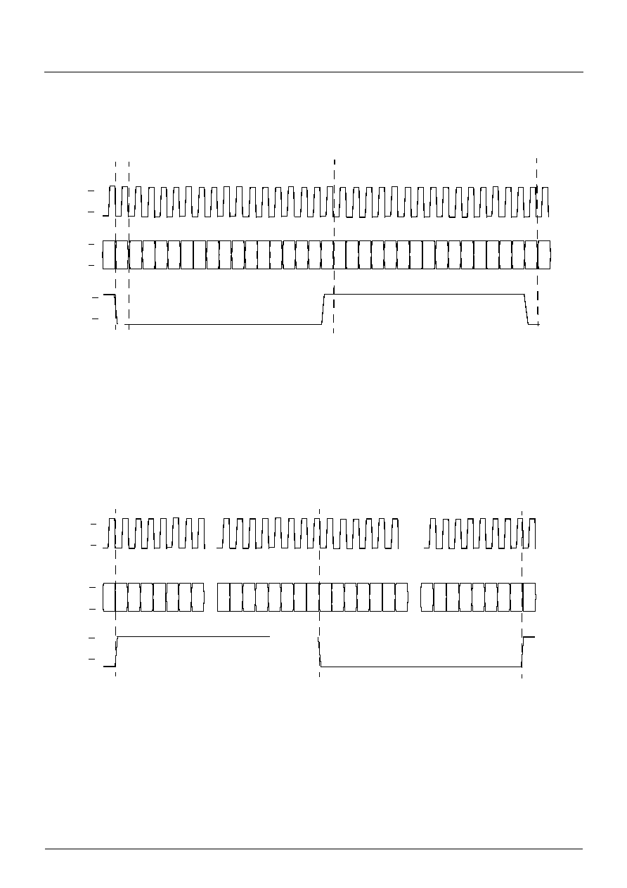
2.6.2. Parallel Data Output
In encoding mode, PIO lines PI12...PI19 are switched
to the MAS 3504D data output which hence will be an
8-bit parallel output port with MSB first (at position
PI19) for the G.729 bit stream data.
The data is transferred in bursts of 10 bytes (1 frame)
each 10 ms. If the transmission of headers is enabled,
there is an additional 10 byte burst before each
sequence of 50 frames.
Handshaking for PIO output mode is accomplished
through the RTW, PCS, and PI12..PI19 signal lines
(see Fig. 2≠3). The PR line has to be set to high level.
RTW will go low as soon as a byte is available in the
output buffer and will stay low until a byte has been
read. Reading of a byte is performed with a PCS
pulse. Data is latched out from the MAS 3504D on the
falling edge of PCS and removed from the bus on the
rising edge of PCS.
Fig. 2≠3: Parallel Data Output (PIO) Timing
> 0.9 V
WSEN > 2 V
DCEN
=1
DSP
operation
µController
DC/DC
On
button
RTW
PIxx
PCS
t
3
t
0
t
1
t
2
t
4
t
5

MAS 3504D
Micronas
9
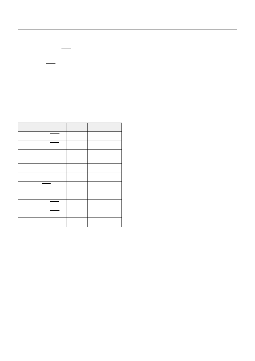
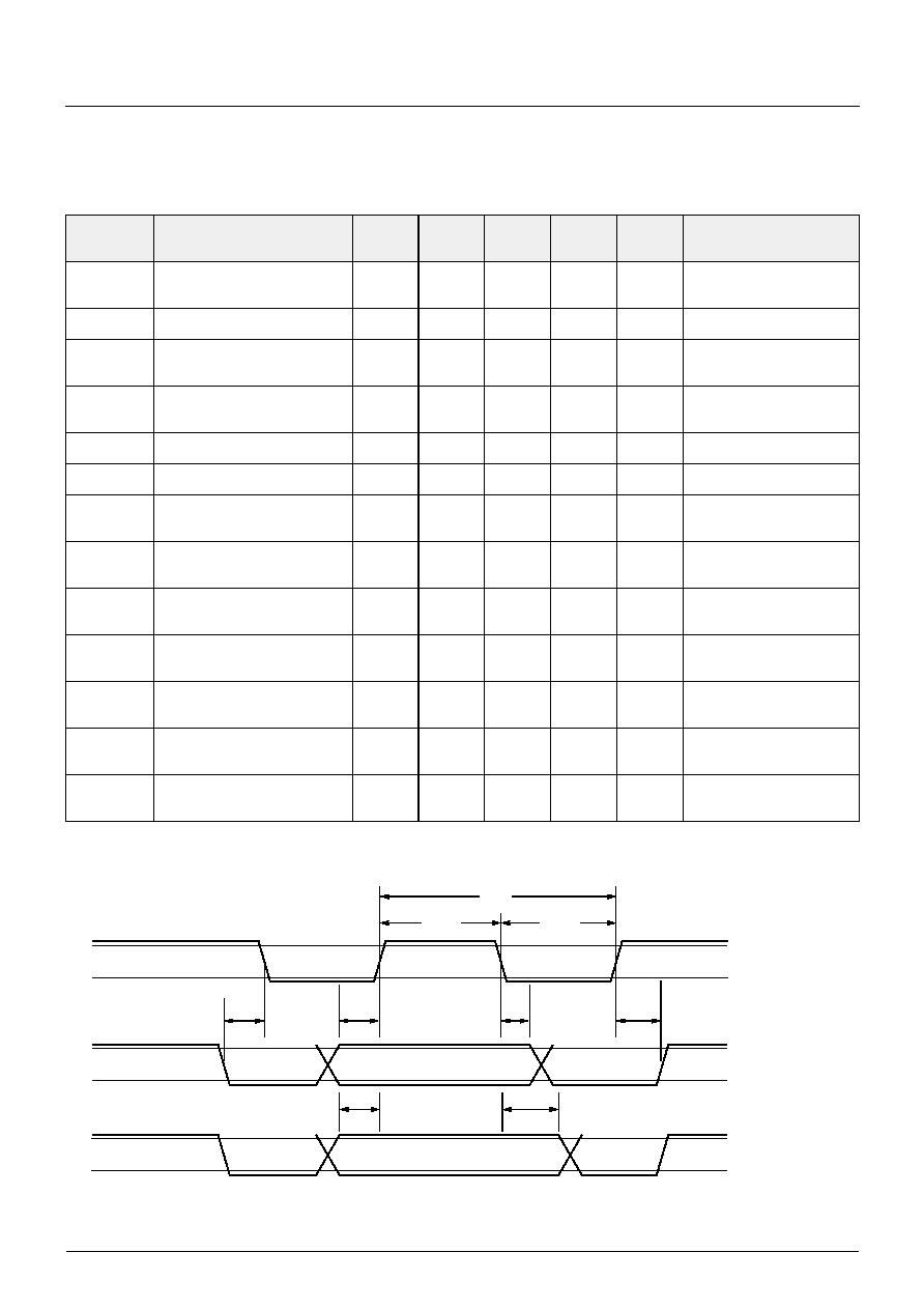
2.6.3. Parallel Data Input
In decoding mode, PIO lines PI12...PI19 are switched
to the MAS 3504D data input which hence will be an 8-
bit parallel input port with MSB first (at position PI19)
for the G.729 bit stream data. In order to write data to
this parallel port, a special handshake protocol has to
be used by the controller (see Fig. 2≠4).
2.6.3.1. DMA Handshake Protocol
The data transfer can be started after the EOD pin of
the MAS 3504D is set to high. After verifying this, the
controller indicates the transmission of data by activat-
ing the PR line. The MAS 3504D responds by setting
the RTR line to the low level. The MAS 3504D reads
the data PI[19:12] after the rising edge of the PR. The
next data word write operation will again be initialized
by setting the PR line via the controller. Please refer to
Figure 2≠4 and Table 2≠2 for the exact timing.
Fig. 2≠4: Handshake protocol for writing G.729 data to the PIO-DMA
Table 2≠1: PIO Output Mode Timing
1)
Symbol
Pin Name
Min.
Max.
Unit
t
0
RTW, PCS
0.010
1800
µ
s
t
1
PCS
0.330
µ
s
t
2
PCS, RTW
0.010
µ
s
t
3
RTW
0.330
10000
µ
s
t
4
PI
0.330
µ
s
t
5
PI
0.081
µ
s
1)
see Figure 2≠3
EOD
PR
RTR
PI[19:12]
high
low
high
low
high
low
high
low
t
st
t
rpr
t
rtrq
t
set
t
h
t
r
t
pr
t
pd
t
eodq
t
eod
Byte 15
Byte 1
MAS 3504D latches the PIO DATA
MAS 3504D
10
Micronas
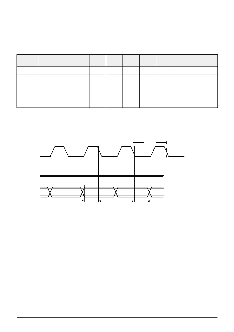
2.6.3.2. End of DMA Transfer
The above procedure will be repeated until the
MAS 3504D sets the EOD signal to "0", which indi-
cates that the transfer of one data block has been exe-
cuted. Subsequently, the controller should set PR to
"0", wait until EOD rises again, and then repeat the
procedure ((see Section 2.6.3.1. on page 9)) to send
the next block of data. The DMA buffer is 10 bytes long
(one frame).
The recommended PIO DMA conditions and the char-
acteristics of the PIO timing are given in Table 2≠2.
2.6.4. Audio Input Interface (SDI)
The A/D interface is a standard I
2
S interface (16/32 bit,
stereo). This input is used for G.729 recording mode
and must be slaved to the D/A output clock and word-
strobe signals.
The interface is configurable by software to work in dif-
ferent modes. It is possible to choose:
≠ inverted or non inverted word strobe (SOI),
≠ no delay or delay of data related to word strobe
≠ inverted or non inverted I
2
S-Clock (SOC).
For further details see Section 3.5.4. on page 18
2.6.5. Audio Output Interface (SDO)
The audio output interface of the MAS 3504D is a
standard I
2
S interface. As the G.729 standard is only
working on mono signals, the same signal is written to
both output channels (left and right).
The interface is configurable by software to work in dif-
ferent modes. It is possible to choose:
≠ 16 or 32 bit/sample modes,
≠ inverted or non inverted word strobe (SOI),
≠ no delay or delay of data related to word strobe
≠ inverted or non inverted I
2
S-clock (SOC).
For further details see Section 3.5.4. on page 18
Table 2≠2: PIO DMA Timing
Symbol
PIO Pin
Min.
Max.
Unit
t
st
PR, EOD
0.010
2000
µ
s
t
r
PR, RTR
40
160
ns
t
pd
PR,
PI[19:12]
120
480
ns
t
set
PI[19:12]
160
no limit
ns
t
h
PI[19:12]
160
no limit
ns
t
rtrq
RTR
200
30000
ns
t
pr
PR
480
no limit
ns
t
rpr
PR, RTR
40
no limit
ns
t
eod
PR, EOD
40
160
ns
t
eodq
EOD
2.5
500
µ
s
MAS 3504D
Micronas
11
2.6.5.1. Example 1:16 Bits/Sample (I
2
S Compatible Data Format)
A schematic timing diagram of the SDO interface in 16 bit/sample mode with delayed data by 1 clock cycle is shown
in Fig. 2≠5.
Fig. 2≠5: Schematic timing of the SDO interface in 16bit/sample mode
2.6.5.2. Example 2:32 Bit/Sample (Inverted SOI)
If the serial output generates 32 bits per audio sample, only the first 20 bits will carry valid audio data. The 12 trailing
bits are set to zero by default (see Fig. 2≠6).
Fig. 2≠6: Schematic timing of the SDO interface in 32 bit/sample mode
SOC
SOD
SOI
left 16-bit audio sample
right 16-bit audio sample
15 14 13 12 11 10 9
8
7
6
5
4
3
2
1
0
13 12 11 10 9 8
7
6 5 4
3
2
1
0
15 14
V
h
V
l
V
h
V
l
V
h
V
l
30 29 28 27 26 25
...
7
6
5
4
3
2
1
0
31 30 29 28 27 26 25
7
6
5
4
3
2
1
0
left 32-bit audio sample
right 32-bit audio sample
SOC
SOD
SOI
V
h
V
l
V
h
V
l
V
h
V
l
...
...
31
...
MAS 3504D
12
Micronas
3. Control Interfaces
3.1. I
2
C Bus Interface
The MAS 3504D is controlled via the I
2
C bus slave
interface.
3.1.1. Device Address and Subaddresses
The IC is selected by transmitting the MAS 3504D
device addresses. (see Table 3≠1).
Writing is done by sending the device write address,
(
3A
hex
) followed by the subaddress byte (
68
hex
) and
two or more bytes of data. Reading is done by sending
the write device address (3A
hex
), followed by the sub-
address byte (69
hex
). Without sending a stop condi-
tion, reading of the addressed data is completed by
sending the device read address (3B
hex
) and reading
n-bytes of data.
By means of the RESET bit in the CONTROL register,
the MAS 3504D can be reset by the controller.
Due to the internal architecture of the MAS 3504D, the
IC cannot react immediately to an I
2
C request. The
typical response time is about 0.5 ms. If the
MAS 3504D cannot accept another complete byte of
data, it will hold the clock line I2C_CL LOW to force the
transmitter into a wait state. The positions within a
transmission where this may happen are indicated by
'Wait' in Section 3.3. on page 14. The maximum wait
period of the MAS 3504D during normal operation
mode is less than 4 ms.
Fig. 3≠1: I
2
C bus protocol (MSB first; data must be stable while clock is high)
Note: S =
I
2
C-Bus Start Condition from master
P =
I
2
C-Bus Stop Condition from master
A =
Acknowledge-Bit: LOW on I2C_DA from slave or master
N =
Not Acknowledge-Bit: HIGH on I2C_DA from master to indicate `End of Read'
Wait =
I
2
C-Clock line is held low, while the MAS 3504D is processing the I
2
C command. This waiting time is
max. 1 ms
Table 3≠1: I
2
C Bus Device Addresses
MAS 3504D device
address
Write
Read
MAS_I2C_ADR
3A
hex
3B
hex
Table 3≠2: Control Register (Subaddress: 6A
hex
)
Name
Subaddress
Bit [8]
Bit : 0-7,
9-15
CONTROL
6A
hex
1 : Reset
0 : normal
0
Table 3≠3: I
2
C Bus Subaddresses
Name
Binary Value
Hex Value
Mode
Function
CONTROL_MAS
0110 1010
6A
hex
Write
control subaddress (see Table 3≠2)
WR_MAS
0110 1000
68
hex
Write
write subaddress
RD_MAS
0110 1001
69
hex
Write
read subaddress
1
0
S
P
I2C_DA
I2C_CL
MAS 3504D
Micronas
13
3.2. Command Structure
The I
2
C control of the MAS 3504D is done completely
via the I
2
C data register by using a special command
syntax. The commands are executed by the
MAS 3504D during its normal operation without any
loss or interruption of the incoming data or outgoing
audio data stream. These I
2
C commands allow the
controller to access internal states, RAM contents,
internal hardware control registers, and to download
software modules. The command structure allows
sophisticated control of the MAS 3504D. The registers
of the MAS 3504D are either general purpose, e.g. for
program flow control, or specialized registers that
directly affect hardware blocks. The unrestricted
access to these registers allows the system controller
to overrule the firmware configuration.
The MAS 3504D firmware scans the I
2
C interface peri-
odically and checks for pending or new commands.
Table 3≠4 on page 13 shows the basic controller com-
mands that are available by the MAS 3504D.
3.2.1. Conventions for the Command Description
The description of the various controller commands
uses the following formalism:
≠ A data value is split into 4-bit nibbles which are
numbered beginning with 0 for the least significant
nibble.
≠ Data values in nibbles are always shown in hexa-
decimal notation indicated by a preceding $.
≠ A hexadecimal 20-bit number d is written, e.g. as
d = $17C63, its five nibbles are
d0 = $3, d1 = $6, d2 = $C, d3 = $7, and d4 = $1.
≠ Abbreviations used in the following descriptions:
a
address
d
data value
n
count value
o
offset value
r
register number
x
don't care
≠ Variables used in the following descriptions:
dev_write
$3A
dev_read
$3B
data_write
$68
data_read
$69
Table 3≠4: Basic Controller Commands
Code
[hex]
Command
Comment
0
1
run
Start execution of an internal program. (Run 0 means freeze operating sys-
tem.)
9
write register
An internal register of the MAS 3504D can be written directly to by the con-
troller.
A
B
write to memory
A block of the DSP memory can be written to by the controller. This feature
may be used to download alternate programs.
D
read register
The controller can read an internal register of the MAS 3504D.
E
F
read memory
A block of the DSP memory can be read by the controller.
MAS 3504D
14
Micronas
3.3. Detailed MAS 3504D Command Syntax
3.3.1. Run
The `run' command causes the start of a program part
at address a = (a3, a2, a1, a0). The nibble a3 is
restricted to 0
hex
or 1
hex
which also acts as command
selector. Run with address a = 0
hex
will suspend the
encoding/decoding function and only I
2
C commands
are evaluated. This freezing is required if alternative
software is downloaded into the internal RAM of the
MAS 3504D. Detailed information about downloading
is provided in combination with a MAS 3504D software
development package or together with MAS 3504D
software modules available from Micronas.
Example: `run' at address 1
hex
(start of G.729 decoder)
has the following I
2
C protocol:
<$3A><$68><$00><$01>
3.3.2. Write Register
The controller writes the 20-bit value
(d = d4, d3, d2, d1, d0) into the MAS 3504D register
(r = r1,r0). In contrast to memory cells, registers are
always addressed individually, and they may also
interact with built-in hardware blocks. A list of registers
is given in Section 3.5. on page 16
Example: G.729 decoding is started by writing the
value 1 into the register with the number FD
hex
:
<$3A><$68><$9F><$D1><$00><$00>
3.3.3. Write D0 Memory
The MAS 3504D has 2 memory areas of 2048 words
each called D0 and D1 memory. For both memory
areas, read and write commands are provided.
Example: writing one word to address d0:0321
hex
has
the following I
2
C protocol:
<$3A><$68><$A0><$00> (write D0 memory)
<$00><$01>
(1 word to write)
<$03><$21> (start
address)
<$23><$45> (value
=
12345
hex
)
<$00><$01>
3.3.4. Write D1 Memory
For further details, see `write D0 memory' command.
S
DW
data_write
W
A
A
A
W
A
P
a3,a2
a1,a0
S
DW
data_write
W
A
A
A
W
A
9,r1
r0,d4
A
W
A
P
d4,d3
d2,d1
S
DW
data_write
A,0
$0,$0
P
n3,n2
n1,n0
a3,a2
a1,a0
d3,d2
d1,d0
d3,d2
d1,d0
....repeat for n data values....
W
A
A
A
W
A
A
W
A
A
W
A
A
W
A
A
W
$0,$0
$0,d4
A
A
W
$0,$0
$0,d4
A
A
W
A
n3..n0: number of words to be transmitted
a3..a0: start address in MASD memory
d4..d0: data value
S
DW
data_write
B,0
$0,$0
P
n3,n2
n1,n0
a3,a2
a1,a0
d3,d2
d1,d0
d3,d2
d1,d0
....repeat for n data values....
W
A
A
A
W
A
A
W
A
A
W
A
A
W
A
A
W
$0,$0
$0,d4
A
A
W
$0,$0
$0,d4
A
A
W
A
n3..n0: number of words to be transmitted
a3..a0: start address in MASD memory
d4..d0: data value

MAS 3504D
Micronas
15
3.3.5. Read Register
The MAS 3504D has an address space of 256 regis-
ters. Some of the registers (r = r1, r0 in the figure
above) are direct control inputs for various hardware
blocks, others do control the internal program flow. In
the next section, those registers that are of any interest
with respect to the G.729 codec are described in
detail.
Example: Read the content of the PIO data register
(C8
hex
):
<$3A><$68><$DC><$80>
<$3A><$69><$3B>
now read:
<d3,d2><d1,d0><x,x><x,d4>
3.3.6. Read D0 Memory
The `read D0 memory' command is provided to get
information from memory cells of the MAS 3504D. It
gives the controller access to all memory cells of the
internal D0 memory. Direct access to memory cells is
an advanced feature of the DSP. It is intended for
users of the MASC software development kit.
3.3.7. Read D1 Memory
The `read D1 memory' command is provided to get
information from memory cells of the MAS 3504D. It
gives the controller access to all memory cells of the
internal D1 memory.
1) send command
2) get register value
S
DW
data_write
D,r1
r0,$0
S
DW
data_read
S
DR
P
P
A
A
N
A
W
A
A
A
W
A
d3,d2
W
x,d4
W
A
W
A
A
d1,d0
W
x,x
A
r1, r0: register r
d3..d0: data value in r
x: don't care
1) send command
2) get memory value
S
DW
data_write
W
A
A
A
W
E,$0
0$,$0
S
DW
data_read
W
A
W
A
d3,d2
S
A
DR
A
d1,d0
P
A
W
n3,n2
n1,n0
A
W
A
P
a3,a2
a1,a0
W
$0,$0
A
$0,d4
W
A
N
d3,d2
A
d1,d0
W
$0,$0
A
$0,d4
....repeat for n data values....
W
W
A
A
A
A
n3..n0: number of words
a3..a0: start address in MASD memory
d4..d0: data value
1) send command
2) get memory value
S
DW
data_write
W
A
A
A
W
F,$0
$0,$0
S
DW
data_read
W
A
W
A
d3,d2
S
A
DR
A
d1,d0
P
A
W
n3,n2
n1,n0
A
W
A
P
a3,a2
a1,a0
W
$0,$0
A
$0,d4
W
A
N
d3,d2
A
d1,d0
W
$0,$0
A
$0,d4
....repeat for n data values....
W
W
A
A
A
A
n3..n0: number of words
a3..a0: start address in MASD memory
d4..d0: data value

MAS 3504D
16
Micronas
3.4. Version Number
Table 3≠5 shows where the chip identification and the
name of the software is located.
3.5. Register Table
In Table 3≠6, the internal registers for controlling the
MAS 3504D are listed. They are accessible by `regis-
ter read/write' I
2
C commands (see Section 3.3. on
page 14). For a more detailed register usage (see
Table 3≠8 on page 19).
Important note! Writing into undocumented registers
or read-only registers is always possible, but it is highly
recommended not to do so. It may damage the func-
tion of the firmware and may even lead to a complete
system crash of the decoder operation which can only
be restored by a reset.
3.5.1. DC/DC Converter (Reg. 8E
hex
)
The DCCF Register controls both, the internal voltage
monitor and the DC/DC converter. Between output
voltage of the DC/DC converter and the internal volt-
age monitor threshold an offset exists which is shown
in Table 3≠8 on page 19. Please pay attention to the
fact, that I
2
C protocol is working only if the processor
works (WSEN = 1).However, the setting for the DCCF
register will remain active if the DCEN and WSEN lines
are deasserted.
The DC/DC converter may generate interference noise
that could be unacceptable for some applications.
Thus the oscillator frequency may be adjusted in 32
steps in order to allow the system controller to select a
base frequency that does not interfere with an other
application.
The CLKI input provides the base clock f
CLKI
for the
frequency divider whose output is made symmetrical
with an additional divider by two. The divider quotient
is determined by the content of the DCCF register.
This register allows 32 settings generating a DC/DC
converter clock frequency f
dc
between:
(EQ 1)
3.5.2. User Control (Reg. FD
hex
)
The UserControl register is used to switch between
basic operation modes. On startup, after a software
reset or a "run 1" command it is set to 0
hex
. The
MAS 3504D sets the control registers to default val-
ues, switches off all interfaces (except I
2
C) and waits
for a change in UserControl.
Table 3≠5: MAS 3504D Version
Addr.
[hex]
Content
Example Value
D1:FF6
name of
MAS 3504D
version
0x03504
3504
D1:FF9
description:
"G.729a CODEC"
0x0472e
G.
D1:FFA
0x03732
72
D1:FFB
0x03961
9A
D1:FFC
0x02043
C
D1:FFD
0x04f44
OD
D1:FFE
0x04543
EC
D1:FFF
0x02020
f
SW
f
C LK I
2
m
n
+
(
)
-------------------------
=
n
0 15
{ ,
} m
32 16
{ ,
}
,

MAS 3504D
Micronas
17
3.5.2.1. Data Transmission Format
The codec is working on a page basis. That means,
that encoding and decoding is performed in blocks of
50 G.729 frames, whereas each frame consists of
10 bytes in byte swapped order (see Fig. 3≠2). There-
fore most changes to the UserControl register become
effective when processing of a page is finished. The
pages are optionally preceeded by 10 byte header
frames (see Table 3≠7).
Switching from encoding to decoding mode or vice
versa directly is not allowed. Instead the controller has
to send a stop request to the MAS 3504D (writing 0
hex
to UserControl). Then the controller has to keep on
sending data in decoding mode or receive data in
encoding mode until the current page of 50 frames is
finished. After this run out time, the encoding or decod-
ing can be started again.
3.5.2.2. Encoder Operation
To enable the G.729 encoder mode, a special routine
has to be downloaded to the MAS 3504D IC first. This
has to be done with an I
2
C download before the
encoder is started the first time. If the encoder is
started without downloading the routine, the behavior
of the IC is unpredictable.
To switch to encoder operation mode, UserControl has
to be set to 3
hex
. Then 50 frames are encoded and
sent via the PIO interface. This is repeated until the
UserControl register is changed. If the transmission of
headers is enabled, each page of 50 frames is pre-
ceeded by a header frame as shown in Table 3≠7.
To switch off the encoder, UserControl has to be set to
0
hex
. Then the encoding and sending of frames contin-
ues until the end of the current page and the operation
mode is set to stop.
3.5.2.3. Decoder Operation
The routines for the G.729 decoder mode are com-
pletely located in the MAS 3504D firmware. So there is
no need to download the encoder routine in a decode
only application.
To switch to decoder operation mode, UserControl has
to be set to 1
hex
. For decoding with slow speed, set
UserControl to 11
hex
. For decoding with fast speed, set
UserControl to 21
hex
. Then the decoder is requesting
several frames via the PIO interface to fill its internal
buffer. If enough data is available, 50 frames are
decoded. This is repeated until the UserControl regis-
ter is changed. If the transmission of headers is
enabled, a header frame (as shown in Table 3≠7) has
to be sent before each page of 50 frames.
To switch off the decoder, UserControl has to be set to
0
hex
. Then the decoding of frames continues until the
end of the current page and the operation mode is set
to stop.
Table 3≠6: Command Register Table
Address
(hex)
Mode
Function
Default
(hex)
Name
8E
w
DC/DC operation control
8000
DCCF
FD
r/w
Operation mode selection
0
UserControl
FC
r/w
Output volume
7FFFF
Volume
74
r/w
Serial interface wordlength
0
Wordlength
E1
r/w
Configuration of the I
2
S audio input interface
4
InputConfig
61
r/w
Configuration of the I
2
S audio output interface
4000
OutputConfig
FA
r/w
Special operation options
0
HWControl
Table 3≠7: Content of Page Header
Byte
1
2
3
4
5
6
7
8
9
10
Value
[hex]
64
6D 72
31
64
61
74
61
F4
01

MAS 3504D
18
Micronas
3.5.2.4. Pause and Mute
If the pause bit is set, the processing continues until
the current page is finished and then en-/decoding is
paused. The pause mode lasts until the pause bit is
cleared again or the mode is set to 0.
If the mute bit is set, the output is muted immediately.
Note that the other bits of the UserControl register
have to stay on their old values when switching to
pause mode.
3.5.3. Volume Control (Reg. FC
hex
)
Volume control is implemented in the MAS 3504D. It
allows to adjust the output volume linear from 0
hex
(silence) to 7FFFF
hex
(original volume).
3.5.4. Interface Control
All the interface control registers have to be written
before the encoder or decoder is started by writing to
the UserControl register. Otherwise they have no
effect until the operation mode is changed.
3.5.4.1. Wordlength Control (Reg. 74
hex
)
A value of 0
hex
sets wordlength on SDI and SDO inter-
faces to 32 bit. 1
hex
sets wordlength to 16 bit.
3.5.4.2. Input Configuration (Reg. 61
hex
)
The content of this register is set on startup by the
firmware. Additional to the Wordlength setting for the
serial interfaces, some other settings can be made.
3.5.4.3. Output Configuration (Reg. E1
hex
)
The content of this register is set on startup by the
firmware. Additional to the Wordlength setting for the
serial interfaces, some other settings can be made.
3.5.5. Hardware Control (Reg. FA
hex
)
The HWControl register is used to set special opera-
tion options.
If the page headers bit is 0, a header frame is trans-
ferred in front of each page of 50 data frames. If the
header bit is 1, all the frames are G.729 data frames.
Bits 2 and 1 are used to select input channels for
encoding. If both bits are set to 0, the left and right
channel are added to get the mono input signal. If only
one of this bits is 1, only the corresponding channel is
used as input.
Fig. 3≠2: Schematic timing of the data transmission with preceeding header
...
...
...
10ms 10ms ...
...
header
page frame
1
frame
2
frame
3
frame
49
frame
49
header
page frame
51
frame
52
frame
99
frame
100 header
page frame
101
frame
102
$64 $6d $72 $31 $64 $61 $74 $61 $f4 $01
byte
2
byte
1
byte
4
byte
3
byte
6
byte
5
byte
8
byte
7
byte
10
byte
9

MAS 3504D
Micronas
19
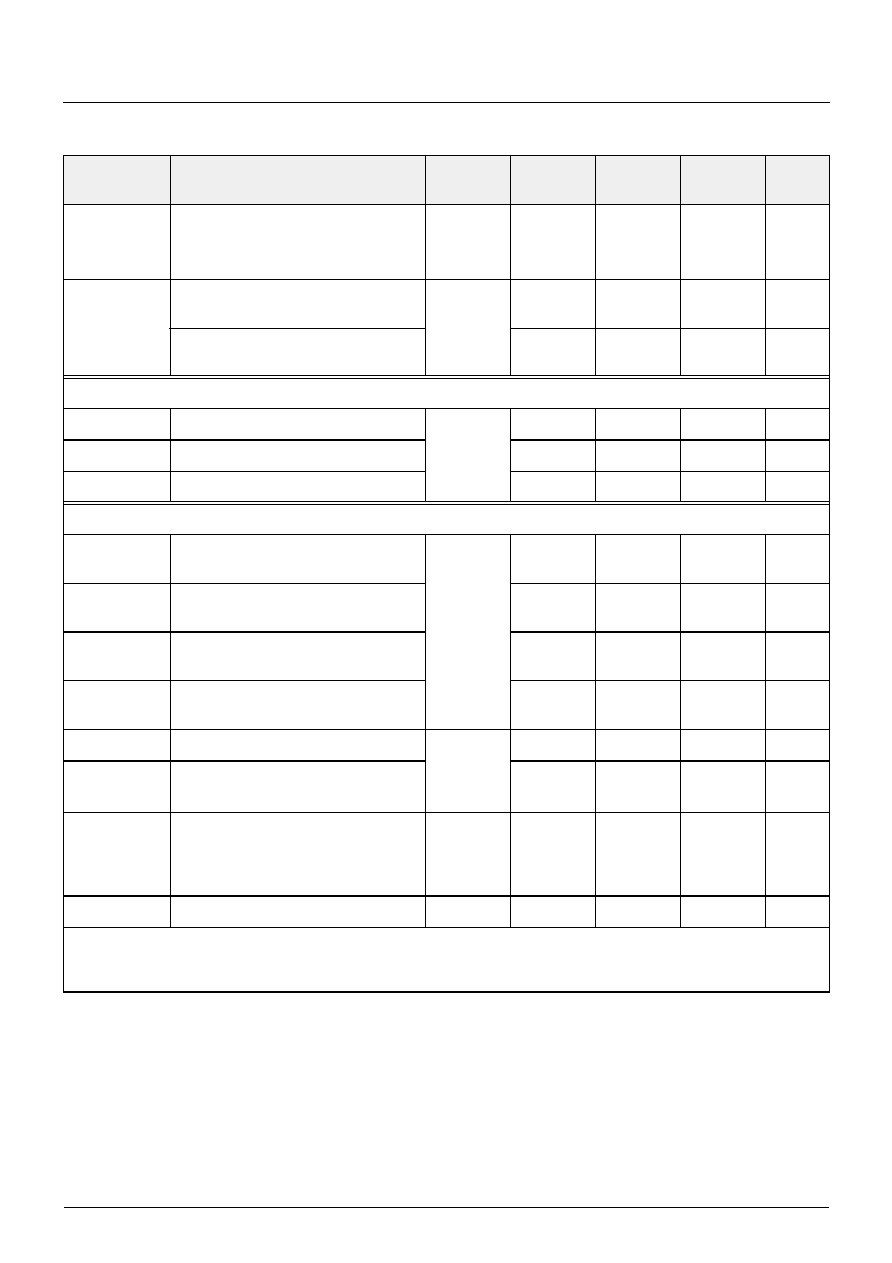
Table 3≠8: Detailed Register Usage
Address
(hex)
Mode
Function
Default
(hex)
Name
61
r/w
Configuration of the I
2
S audio input interface
bit[19:12]
not used, set to 0
bit[11]
additional delay of data related to word strobe
0
no delay
1
1 bit delay
bit[10:6]
not used, set to 0
bit[5]
input word strobe signal
0
standard timing
1
inverted timing
bit[4:3]
not used, set to 0
bit[2]
input clock signal
0
standard timing
1
inverted timing
bit[1:0]
not used, set to 0
4
InputConfig
74
r/w
Serial output interface wordlength
bit[19:1]
not used, set to 0
bit[0]
wordlength
0
32 bit/sample
1
16 bit/sample
0
Wordlength
MAS 3504D
20
Micronas
8E
w
DC/DC operation control
bit[19:17]
not used, set to 0
bit[16:14,9] output voltage / internal voltage monitor
(PUP signal becomes inactive when output
is below the monitoring voltage)
8000
DCCF
Setting
bit [16:14] and [9]
DC/DC-Converter
Output Voltage [V]
Internal Monitor
Voltage [V]
1 11
0
1 10 0
1 01 0
1 00 0
0 11
0
0 10 0
0 01 0
0 00 0
1 11
1
1 10 1
1 01 1
1 00 1
0 11
1
0 10 1
0 01 1
0 00 1
3.57
3.46
3.35
3.25
3.14
3.04
2.94
2.83
2.73
2.63
2.52
2.42
2.32
2.22
2.12
2.02
3.38
3.27
3.16
3.06
2.95
2.85
2.75
2.64
2.54
2.44
2.33
2.23
2.13
2.03
1.93
1.82
bit[13:10,8] DC/DC-converter switching frequency f
SW
[kHz]
Setting
bit [13:10]
Frequency/kHz
bit [8] = 0
Frequency/kHz
bit [8] = 1
11 11
11 10
11 01
11 00
10 11
10 10
10 01
10 00
01 11
01 10
01 01
01 00
00 11
00 10
00 01
00 00
156
160
163
167
171
175
179
184
188
194
199
204
210
216
223
230
128
245
253
263
272
283
295
307
320
335
351
368
387
409
433
460
bit[7:0]
not used, set to 0
Table 3≠8: Detailed Register Usage, continued
Address
(hex)
Mode
Function
Default
(hex)
Name
MAS 3504D
Micronas
21
E1
r/w
Configuration of the I
2
S audio output interface
bit[19:15]
not used, set to 0
bit[14]
output clock signal
0
standard timing
1
inverted timing
bit[13:12]
not used, set to 0
bit[11]
additional delay of data related to word strobe
0
no delay
1
1 bit delay
bit[10:6]
not used, set to 0
bit[5]
output word strobe signal
0
standard timing
1
inverted timing
bit[4:0]
not used, set to 0
4000
OutputConfig
FA
r/w
Special operation options
bit[19:3]
not used, set to 0
bit[2:1]
input channel matrixing
00
add left/right channel
01
input only from right channel
10
input only from left channel
11
not allowed
bit[0]
page headers
0
enable
1
disable
0
HWControl
FC
r/w
Output volume
bit[19:0]
linear volume level
7FFFF
Volume
FD
r/w
Operation mode selection
bit[19:6]
not used, set to 0
bit[5:4]
decoding speed
00
8 kHz (normal)
01
6 kHz (slow)
10
12 kHz (fast)
11
not allowed
bit[3]
mute audio output
0
disable
1
enable
bit[2]
pause encoder/decoder
0
disable
1
enable
bit[1:0]
mode
00
idle
01
decode
10
not allowed
11
encode
0
UserControl
Table 3≠8: Detailed Register Usage, continued
Address
(hex)
Mode
Function
Default
(hex)
Name
MAS 3504D
22
Micronas
4. Specifications
4.1. Outline Dimensions
Fig. 4≠1:
Plastic Metric Quad Flat Pack 44-Pin
(PMQFP44)
Weight approximately 0.4 g
Dimensions in mm
Fig. 4≠2:
Low-Profile Fine-Pitch Ball Grid Array 49-Pin
(LFBGA49)
Weight approximately 0.13 g
Dimensions in mm
SPGS706000-5(P44)/1E
34
44
1
11
12
22
23
33
0.1
0.8
0.8
13.2
0.2
±
13.2
0.2
±
0.17
0.06
±
2.15
0.2
±
2.0
0.1
±
0.34
0.05
±
10
0.1
±
10
0.1
±
10 x 0.8 = 8
0.1
±
10 x 0.8 = 8
0.1
±
0.46
6 x 0.8 = 4.8
SPGS708000-1(P49)/1E
7
0.8
7
6 x 0.8 = 4.8
0.8
A
B
C
D
E
F
G
1
2
3
4
5
6
7
1.4
0.36
A1 Ball Pad Corner
Laser marked pin 1
MAS 3504D
Micronas
23
4.2. Pin Connections and Short Descriptions
NC
not connected, leave vacant
LV
If not used, leave vacant
X
obligatory, pin must be connected as described
in application information
VDD connect to positive supply
VSS connect to ground
Pin No.
Pin Name
Type
Connection
Short Description
PMQFP
44-pin
LFBGA
49-ball
Test Alias in ()
(If not used)
1
C3
TE
IN
VSS
Test Enable
2
C2
POR
IN
X
Reset, Active Low
3
B1
I2CC
IN/OUT
X
I
2
C Clock Line
4
D2
I2CD
IN/OUT
X
I
2
C Data Line
5
C1
VDD
SUPPLY
X
Positive Supply for Digital Parts
6
D1
VSS
SUPPLY
X
Ground Supply for Digital Parts
7
E2
DCEN
IN
VSS
Enable DC/DC Converter
8
E1
EOD
OUT
LV
PIO End of DMA, Active Low
9
F2
RTR
OUT
LV
PIO Ready to Read, Active Low
10
F1
RTW
OUT
LV
PIO Ready to Write, Active Low
11
G1
DCSG
SUPPLY
VSS
DC Converter Transistor Ground
12
E3
DCSO
OUT
VSS
DC Converter Transistor Open Drain
13
F3
VSENS
IN
VDD
DC Converter Voltage Sense
14
G2
PR
IN
X
PIO-DMA Request or Read/Write
15
F4
PCS
IN
X
PIO Chip Select, Active Low
16
G3
PI19
IN/OUT
LV
PIO Data [19]
data bit [7], MSB
17
E4
PI18
IN/OUT
LV
PIO Data [18]
data bit [6]
18
G4
PI17
IN/OUT
LV
PIO Data [17]
data bit [5]
19
F5
PI16
IN/OUT
LV
PIO Data [16]
data bit [4]
20
G5
PI15
IN/OUT
LV
PIO Data [15]
data bit [3]
21
F6
PI14
IN/OUT
LV
PIO Data [14]
data bit [2]
22
G6
PI13
IN/OUT
LV
PIO Data [13]
data bit [1]
23
E5
PI12
IN/OUT
LV
PIO Data [12]
data bit [0]
24
E6
SOD
(PI11)
OUT
LV
Serial Output Data
25
F7
SOI
(PI10)
OUT
LV
Serial Output Frame Identification
26
D6
SOC
(PI9)
OUT
LV
Serial Output Clock
MAS 3504D
24
Micronas
27
E7
PI8
IN
LV
Not used
28
D7
XVDD
SUPPLY
X
Positive Supply of Output Buffers
29
C6
XVSS
SUPPLY
X
Ground of Output Buffers
30
C7
SID
(PI7)
IN
VSS
Serial Input Data
31
B6
SII
(PI6)
IN
VSS
Serial Input Frame Identification
32
B7
SIC
(PI5)
IN
VSS
Serial Input Clock
33
A7
PI4
IN
LV
Not used
34
B5
PI3
IN
LV
Not used
35
A6
PI2
IN
LV
Not used
36
B4
PI1
IN
LV
Not used
37
A5
PI0
IN
LV
Not used
38
C4
CLKO
OUT
LV
Not used
39
A4
PUP
OUT
LV
Power Up (status of voltage supervision)
40
B3
WSEN
IN
X
Enable DSP and Start DC/DC Converter
41
A3
WRDY
OUT
LV
If WSEN = 0: valid clock input at CLKI
If WSEN = 1: clock synthesizer PLL
locked
42
B2
AVDD
SUPPLY
VDD
Supply for Analog Circuits
43
A2
CLKI
IN
X
Clock Input
44
A1
AVSS
SUPPLY
VSS
Ground Supply for Analog Circuits
Pin No.
Pin Name
Type
Connection
Short Description
PMQFP
44-pin
LFBGA
49-ball
Test Alias in ()
(If not used)

MAS 3504D
Micronas
25
4.2.1. Pin Descriptions
4.2.1.1. Power Supply Pins
Connection of all power supply pins is mandatory for
the function of the MAS 3504D.
VDD
SUPPLY
VSS
SUPPLY
The VDD/VSS pair is internally connected with all digi-
tal modules of the MAS 3504D.
XVDD
SUPPLY
XVSS
SUPPLY
The XVDD/XVSS pins are internally connected with
the pin output buffers.
AVDD
SUPPLY
AVSS
SUPPLY
The AVDD/AVSS pair is connected internally with the
analog blocks of the MAS 3504D, i.e. clock synthe-
sizer and supply voltage supervision circuits.
4.2.1.2. DC/DC Converter Pins
DCEN
IN
The DCEN input signal enables the DC/DC converter
operation.
DCSG
SUPPLY
The `DC converter Signal Ground' pin is used as a
basepoint for the internal switching transistor of the
DC/DC converter. It must always be connected to
ground.
DCSO
OUT
DCSO is an open drain output and should be con-
nected with external circuitry (inductor/diode) to start
the DC/DC converter. When the DC/DC converter is
not used, it has to be connected to VSS.
VSENS
IN
The VSENS pin is the input for the DC/DC converter
feedback loop. It must be connected directly with the
Schottky diode and the capacitor as shown in Fig. 2≠1
on page 7.
When the DC/DC converter is not used, it has to be
connected to VDD.
4.2.1.3. Control Lines
I2CC
SCL
IN/OUT
I2CD
SDA
IN/OUT
Standard I
2
C control lines. Normally there are Pull-up-
resistors tied from each line to VDD.
4.2.1.4. Parallel Interface Lines
4.2.1.4.1. PIO Handshake Lines
'PIO handshake lines' are used in operation mode.
PIO-DMA mode is used in input mode and
µ
P mode in
output mode.
PCS
IN
The 'PIO chip select'
is
driven from microcontroller to
activate data output from MAS 3504D to the bus. Data
is output to the bus on the falling edge of PCS and is
removed on the rising edge of PCS.
PR
IN
The 'PIO request' must be set to `1' to validate data
output from MAS 3504D.
RTR
OUT
`Ready to read' is driven from the MAS 3504D in PIO/
DMA input mode.
RTW
OUT
`Ready to write' is driven from MAS 3504D to indicate
that data is available in PIO output mode.
EOD
OUT
`End of DMA' is supported by the built-in firmware in
PIO-DMA input mode.
4.2.1.4.2. PIO Data Lines
PI19...PI12
PARALLEL DATA
OUT/IN
These pins are used to send or receive compressed
data.
MAS 3504D
26
Micronas
4.2.1.5. Voltage Supervision And Other Functions
CLKI
IN
This is the clock input of the MAS 3504D. CLKI should
be a buffered output of a crystal oscillator. Standard
clock frequency is 18.432 MHz.
CLKO
OUT
This pin has no function.
PUP
OUT
The PUP
output indicates that the power supply volt-
age exceeds its minimal level (software adjustable).
WSEN
IN
WSEN enables DSP operation and switches on the
DC/DC-converter.
WRDY
OUT
WRDY has two functions depending on the state of the
WSEN signal.
If WSEN = '0', it indicates that a valid clock has been
recognized at the CLKI clock input.
If WSEN = '1', the WRDY output will be set to `0' until
the internal clock synthesizer has locked to the incom-
ing audio data stream, and thus, the CLKO clock out-
put signal is valid.
4.2.1.6. Serial Input Interface
SID
IN
SII
IN
SIC
IN
Data, Frame Indication, and Clock line of the serial
input interface. The SII indicates whether the left or the
right audio sample is transmitted.
4.2.1.7. Serial Output Interface
SOD
OUT
SOI
OUT
SOC
OUT
Data, Frame Indication, and Clock line of the serial
output interface. The SOI indicates whether the left or
the right audio sample is transmitted.
4.2.1.8. Miscellaneous
POR
IN
The Power On Reset pin is used to reset the digital
parts of the MAS 3504D. POR is a low active signal.
TE
IN
The TE pin is for production test only and must be con-
nected with VSS in all applications.
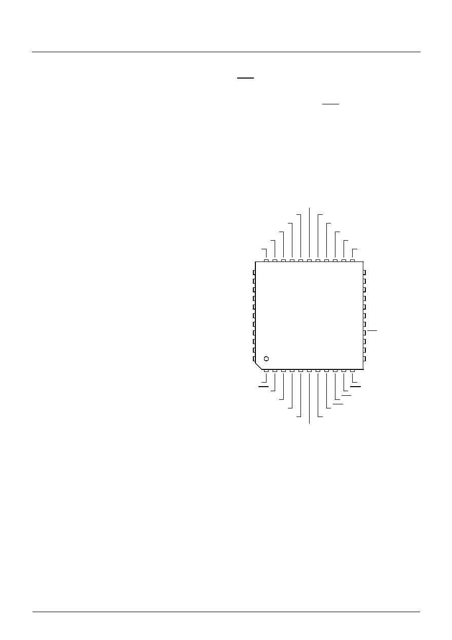
4.2.2. Pin Configurations
Fig. 4≠3: PMQFP44 package
34
35
36
37
38
39
40
41
42
43
44
22
21
20
19
18
17
16
15
14
13
12
1
2
3
4
5
6
7
8
9
10 11
33 32 31 30 29 28 27 26 25 24 23
PI3
PI2
PI1
PI0
CLKO
PUP
WSEN
WRDY
AVDD
CLKI
AVSS
PI13
PI14
PI15
PI16
PI17
PI18
PI19
PCS
PR
VSENS
DCSO
SIC
SII
SID
XVSS
XVDD
PI4
PI8
SOC
SOI
SOD
PI12
POR
I2CC
I2CD
VDD
VSS
TE
DCEN
EOD
RTR
RTW
DCSG
MAS 3504D

MAS 3504D
Micronas
27
4.2.3. Internal Pin Circuits
Fig. 4≠4: Input pins PCS, PR
Fig. 4≠5: Input pin TE, DCEN
Fig. 4≠6: Input pins WSEN, POR
Fig. 4≠7: Input pin CLKI
Fig. 4≠8: Input/Output pins PI0...PI4, PI8, SOC, SOI,
SOD, PI12...PI19
Fig. 4≠9: Input/Output pins I2CC, I2CD
Fig. 4≠10: Input/Output pins DCSO, DCSG
Fig. 4≠11: Output pins WRDY, RTW, EOD, RTR,
CLKO, PUP
Fig. 4≠12: Input pin VSENS
Fig. 4≠13: Input/Output pins SIC, SII, SID
TTLIN
VDD
P
N
VSS
VDD
N
VSS
DCSO
DCSG
VSS
VDD
VSS
N
P
VSENS
VSS
VDD
P
N
VSS

MAS 3504D
28
Micronas
4.2.4. Electrical Characteristics
4.2.4.1. Absolute Maximum Ratings
Stresses beyond those listed in the "Absolute Maximum Ratings" may cause permanent damage to the device. This
is a stress rating only. Functional operation of the device at these or any other conditions beyond those indicated in
the "Recommended Operating Conditions/Characteristics" of this specification is not implied. Exposure to absolute
maximum ratings conditions for extended periods may affect device reliability.
Symbol
Parameter
Pin
Name
Min.
Max.
Unit
T
A
Ambient operating temperature
- operating conditions
- extended temperature range
1)
0
-
30
85
85
∞C
T
C
Case operating temperature
- LFBGA49
- PMQFP44
0
0
95
95
∞C
T
S
Storage temperature
-
40
125
∞C
P
MAX
Power dissipation
for all packages
VDD,
XVDD,
AVDD
400
mW
V
SUP
Supply voltage
VDD,
XVDD,
AVDD
5.5
V
V
Idig
Input voltage, all digital inputs
-
0.3
V
SUP
+0.3
V
I
Idig
Input current, all digital inputs
-
20
+20
mA
VII2C
Input Voltage, I
2
C-Pins
I2CC
I2CD
-
0.3
5.5
V
I
Out
Current, all digital outputs
0.5
A
I
OutDC
Current
DCSO
1.5
A
1)
The functionality of the device in the "extended temperature range" was checked by electrical characterization
on sample base. Data sheet parameters are valid for "operating conditions" only.
MAS 3504D
Micronas
29
4.2.4.2. Recommended Operating Conditions
Symbol
Parameter
Pin
Name
Min.
Typ.
Max.
Unit
T
A
Ambient operating temperature
- operating conditions
- extended temperature range
1)
0
-
30
85
85
∞C
∞C
V
SUP
Supply voltage for G.729 decoder
operation and download software
VDD,
XVDD,
AVDD
2.5
3.0
3.6
V
Supply voltage for G.729 encoder
operation
3.0
3.3
3.6
V
Reference Frequency Generation
CLK
F
Clock Frequency
CLKI
18.432
MHz
CLK
I_V
Clock Input Voltage
0
V
SUP
V
CLK
Amp
Clock Amplitude
0.5
V
pp
Levels
I
IL27
Input Low Voltage
@V
SUP
= 2.5 V ... 3.6 V
POR
I2CC,
I2CD,
DCEN,
WSEN
0.4
V
I
IH36
Input High Voltage
@V
SUP
= 2.5 V ... 3.6 V
1.8
V
I
IH33
Input High Voltage
@V
SUP
= 2.5 V ... 3.3 V
1.7
V
I
IH30
Input High Voltage
@V
SUP
= 2.5 V ... 3.0 V
1.6
V
I
ILD
Input Low Voltage
PI<I>
2)
,
SII, SIC,
SID, PR,
PCS, TE,
0.4
V
I
IHD
Input High Voltage
V
SUP
-
0.5
V
T
rf
Rise / Fall time of digital inputs
PI<I>, SII,
SIC, SID,
PR, PCS,
CLKI
10
ns
D
cycle
Duty cycle of clock inputs
SIC, CLKI
40
50
60
%
1)
The functionality of the device in the "extended temperature range" was checked by electrical characterization
on a sample base. Data sheet parameters are valid for "operating conditions" only.
2)
i = 0 to 4, 8 , 12 to 19

MAS 3504D
30
Micronas
4.2.4.3. Characteristics
Typ. values at T
A
= 27 ∞C, V
SUP
= 3.3 V, CLK
F
= 18.432 MHz, duty cycle = 50%
DC-DC converter external circuitry
C
1
Blocking Capacitor
(25 m
ESR)
3)
VSENS,
DCSG
330
µ
F
V
F
Schottky Diode Forward voltage
4)
DCSO,
VSENS
0.35
0.45
V
L
Inductance of Ferrite ring core coil
5)
(50 m
),VAC 616/103
DCSO
20
µ
H
3)
Sanyo Oscon 6SA330M
(distributed by Endrich Bauelemente, D-72202 Nagold-lselshausen, www.endrich.com)
4)
ZETEX ZMCS1000
(distributed by ZETEX, D-81673 M¸nchen,
europe.sales@zetex.com), standard Schottky 1N5817
5)
C8 R/4L, SDS0604 (distributed by Endrich Bauelemente, s.a.), VAC 616/103
Symbol
Parameter
Pin
Name
Min.
Typ.
Max.
Unit
Symbol
Parameter
Pin
Name
Min.
Typ.
Max.
Unit
Test Conditions
Supply Voltage
I
SUP
Current Consumption
VDD,
XVDD,
AVDD
46
mA
3.3 V, G.729 encoding
25
mA
3.3 V, G.729 decoding
15
mA
3.3 V, waiting mode
Digital Outputs and Inputs
V
DOL
Output Low Voltage
PI<I>
1)
,
SOI,
SOC,
SOD,
EOD,
RTR,
RTW,
WRDY,
PUP,
CLKO
0.3
V
@ I
LOAD
= 6 mA
V
DOH
Output High Voltage
V
SUP
-
0.3
V
@ I
LOAD
= 6 mA
C
DIGL
Input Capacitance
PI<I>,
SII,
SIC,
SID,
PR,
PCS,
CLKI
7
pF
I
DLeak
Digital Input Leakage
Current
-
1
1
µ
A
0 V < V
pin
< V
SUP
1)
i = 0 to 4, 8 , 12 to 19
MAS 3504D
Micronas
31
4.2.4.3.1. I
2
C Characteristics
at T
A
=
-
30 to 85 ∞C, V
SUP
= 2.5 to 3.6 V, typ. values at T
A
= 27 ∞C, V
SUP
= 3.3 V, CLK
F
= 18.432 MHz,
duty cycle = 50%
Fig. 4≠14: I
2
C timing diagram
Symbol
Parameter
Pin
Name
Min.
Typ.
Max.
Unit
Test Conditions
R
ON
Output Resistance
I2CC,
I2CD
60
I
LOAD
= 5 mA,
V
SUP
= 2.7 V
f
I2C
I
2
C Bus Frequency
I2CC
400
kHz
t
I2C1
I
2
C START Condition Setup
Time
I2CC,
I2CD
300
ns
t
I2C2
I
2
C STOP Condition Setup
Time
I2CC,
I2CD
300
ns
t
I2C3
I
2
C Clock Low Pulse Time
I2CC
1250
ns
t
I2C4
I
2
C Clock High Pulse Time
I2CC
1250
ns
t
I2C5
I
2
C Data Hold Time before
Rising Edge of Clock
I2CC
80
ns
t
I2C6
I
2
C Data Hold Time after
Falling Edge of Clock
I2CC
80
ns
V
I2COL
I
2
C Output Low Voltage
I2CC,
I2CD
0.3
V
I
LOAD
= 5 mA
I
I2COH
I
2
C Output High Leakage
Current
I2CC,
I2CD
1
uA
V
I2CH
= 3.6 V
t
I2COL1
I
2
C Data Output Hold Time
after Falling Edge of Clock
I2CC,
I2CD
20
ns
t
I2COL2
I
2
C Data Output Setup Time
before Rising Edge of Clock
I2CC,
I2CD
250
ns
f
I2C
= 400 kHz
T
W
Wait time
I2CC,
I2CD
0
0.5
4
ms
I2CC
I2CD as input
I2CD as output
t
I2C1
t
I2C5
t
I2C6
t
I2C2
t
I2C4
t
I2C3
1/f
I2C
t
I2COL2
t
IC2OL1
H
L
H
L
H
L
MAS 3504D
32
Micronas
4.2.4.3.2. I
2
S Bus Characteristics ≠ SDI
at T
A
=
-
30 to 85 ∞C, V
SUP
= 3.0 to 3.6 V, typ. values at T
A
= 27 ∞C, V
SUP
= 3.3 V, CLK
F
= 18.432 MHz,
duty cycle = 50%
Fig. 4≠15: Serial input
Symbol
Parameter
Pin
Name
Min.
Typ.
Max.
Unit
Test Conditions
t
SICLK
I
2
S Clock Input Period
SIC
960
ns
t
SIIDS
I
2
S Data SetupTime before
Falling Edge of Clock
SIC,
SID
50
t
SICLK
-
100
ns
t
SIIDH
I
2
S Data Hold Time
SID
50
ns
t
bw
Burst Wait Time
SIC,
SID
480
H
L
H
L
H
L
T
SICLK
T
SIIDH
T
SIIDS
SIC
SII
SID
MAS 3504D
Micronas
33
4.2.4.3.3. I
2
S Characteristics ≠ SDO
at T
A
=
-
30 to 85 ∞C, V
SUP
= 3.0 to 3.6 V, typ. values at T
A
= 27 ∞C, V
SUP
= 3.3 V, CLK
F
= 18.432 MHz,
duty cycle = 50%
Fig. 4≠16: Serial output SOI
Symbol
Parameter
Pin
Name
Min.
Typ.
Max.
Unit
Test Conditions
t
SOCLK
I
2
S Clock Output Period
SOC
1953
ns
8 kHz stereo
32 bit/sample
t
SOISS
I
2
S Wordstrobe Hold Time
after Falling Edge of Clock
SOC,
SOI
10
t
SOCLK
/
2
ns
t
SOODC
I
2
S Data Hold Time after
Falling Edge of Clock
SOC,
SOD
10
t
SOCLK
/
2
ns
H
L
H
L
H
L
T
SOCLK
T
SOISS
T
SOISS
T
SOODC
SOC
SOI
SOD

MAS 3504D
34
Micronas
4.2.4.4. DC/DC Converter Characteristics
at T
A
=
-
30 to 85 ∞C, V
SUP
= 3.0 V, CLK
F
= 14.725 MHz, f
sw
= 230 kHz, typ. values at T
A
= +27 ∞C
Unless otherwise noted: VOUT = 3.0 V, VIN = 1.2 V
Note: The following characterizations were made with voltage and clock input that is not usable for G.729 applica-
tions.
Symbol
Parameter
Pin Name
Min.
Typ.
Max.
Unit
Test Conditions
V
IN1
Minimum start-up input voltage
1)
0.9
1.1
V
I
LOAD
= 0 mA
DCCF = 08000
hex
(Reset)
V
IN2
Minimum operating input
voltage
1)
0.6
0.9
V
I
LOAD
= 55 mA,
DCCF = 08000
hex
(Reset)
1.3
1.8
V
I
LOAD
= 250 mA,
DCCF = 08000
hex
(Reset)
V
OUT
Output voltage range
Bits 16..14, Bit 9 of DCCF
Register [hex]:
1C000
18000
14000
10000
0C000
08000
04000
00000
1C200
18200
14200
10200
0C200
08200
04200
00200
VSENS
3.567
3.460
3.354
3.248
3.144
3.039
2.935
2.831
2.729
2.625
2.524
2.422
2.321
2.219
2.118
2.017
V
V
IN
= 1.2 V
I
LOAD
= 50 mA
V
OTOL
Output voltage tolerance
VSENS
-
3.6
3.6
%
I
LOAD
= 50 mA
T
j
= 27 ∞C
V
IN
= 1.2 V
I
LOAD1
Output current
VSENS
150
mA
V
IN
= 0.9..1.5 V
I
LOAD2
250
mA
V
IN
= 1.8..3.0 V
dV
OUT
/dV
IN
/
V
OUT
Line regulation
VSENS
0.35
%/V
I
LOAD
= 50mA
dV
OUT
/dV
IN
/
V
OUT
Line regulation
VSENS
0.7
%/V
I
LOAD
= 250 mA,
V
OUT
= 3.5 V,
V
IN
= 2.4 V
dV
OUT
/V
OUT
Load regulation
VSENS
-
0.5
%
I
LOAD
= 50...150 mA,
dV
OUT
/V
OUT
Load regulation
VSENS
-
0.5
%
I
LOAD
= 50..250 mA,
V
OUT
= 3.5 V,
V
IN
= 2.4 V
1)
All measurements are made with a C8 R/4L 20
µ
H, 25 m
ferrite ring-core coil, Zetex ZLMCS1000 Schottky
diode, and Sanyo/Oscon 6SA330M 330
µ
F, 25 m
ESR capacitors at input and output (see Section 4.2.4. on
page 28).

MAS 3504D
Micronas
35
h
max
Maximum efficiency
90
%
V
IN
= 3.0 V,
V
OUT
= 3.5 V
I
SUPPLY
Supply current
VSENS
1.1
5
mA
V
IN
= 3.0 V, I
LOAD
= 0,
includ. switch current
I
L,MAX
Inductor current limit
DCSO,
DCSG
1.0
1.4
A
R
ON
Switch on-resistance
DCSO,
DCSG
0.4
I
LEAK
Switch leakage current
DCSO,
DCSG
0.1
1
µ
A
T
j
= 27
∞
C,
converter = off,
I
LOAD
= 0
µ
A
f
SW
Switch frequency
DCSO,
DCSG
156
230
460
kHz
Depending on DCCF
t
START
Start up time asserting to PUP
DCEN
,
PUP
8
ms
V
IN
= 1.0 V,
I
LOAD
= 1 mA,
PUPLIM = 010 (Reset)
f
STARTUP
VSENSE
DCSO
250
kHz
VSENS < 1.9 V
Symbol
Parameter
Pin Name
Min.
Typ.
Max.
Unit
Test Conditions

MAS 3504D
36
Micronas
4.2.4.5. Typical Performance Characteristics
Fig. 4≠17: Efficiency vs. Load Current
Load Current (A)
0
20
40
60
80
100
Efficiency (%)
Efficiency vs. Load Current
(Vout=2.7V)
Load Current (A)
0
20
40
60
80
100
Efficiency (%)
Efficiency vs. Load Current
(Vout=3.5V)
Load Current (A)
0
20
40
60
80
100
Efficiency (%)
Efficiency vs. Load Current
(Vout=2.2V)
Load Current (A)
0
20
40
60
80
100
Efficiency (%)
Efficiency vs. Load Current
(Vout=3.0V)
10
10
10
10
1
-4
-3
-2
-1
10
10
10
10
1
-4
-3
-2
-1
10
10
10
10
1
-4
-3
-2
-1
10
10
10
10
1
-4
-3
-2
-1
Vin:
2.4V
1.8V
1.5V
1.2V
0.9V
0.7V
Vin:
3.0V
2.4V
1.8V
Vin:
2.4V
1.8V
1.2V
Vin:
1.5V
1.2V
0.9V
0.7V
3.0 V
1.8 V
Vin
0.7 V
2.4 V
Vin
0.7 V
1.5 V
Vin
2.4 V
1.2 V
Vin

MAS 3504D
Micronas
37
Fig. 4≠18: Output Voltage vs. Input Voltage
Fig. 4≠19: Output Voltage vs. Load Current
1.5
2
2.5
3
3.5
Input Voltage (V)
2.6
2.8
3
3.2
3.4
3.6
Output Voltage (V)
Output Voltage vs. Input Voltage
Iload=250mA
0.9
1.4
1.9
2.4
2.9
Input Voltage (V)
2
2.2
2.4
2.6
2.8
3
3.2
Output Voltage (V)
Output Voltage vs. Input Voltage
Iload=50mA
3.5 V
3.1 V
2.7 V
3.1 V
2.2 V
2.7 V
0
0.1
0.2
0.3
Load Current (A)
2.6
2.8
3
3.2
3.4
3.6
Output Voltage (V)
Output Voltage
vs. Load Current
0
0.02
0.04
0.06
0.08
Load Current (A)
2
2.2
2.4
2.6
2.8
3
3.2
3.4
Output Voltage
Output Voltage
vs. Load Current
Vin=3V, 2.4V, 1.8V
Vin=2.4V
Vin=1.5V, 0.9V
Vin=1.5V, 0.9V
Vin
Vin
Vin
MAS 3504D
38
Micronas
Fig. 4≠20: Maximum Load Current vs. Input Voltage
Fig. 4≠21: No Load Supply Current vs. Input Voltage
0 1
2
3
Input Voltage (V)
0
0.2
0.4
0.6
0.8
Maximum Load Current (A)
Maximum Load Current
vs. Input Voltage
Vout=
3.5V
3.1V
2.7V
2.2V
3.5V
2.2V
V
out
0 1
2
3
Input Voltage (V)
0
2.0
4.0
6.0
No Load Supply Current (mA)
No Load Supply Current
vs. Input Voltage
V
out
= 3 V
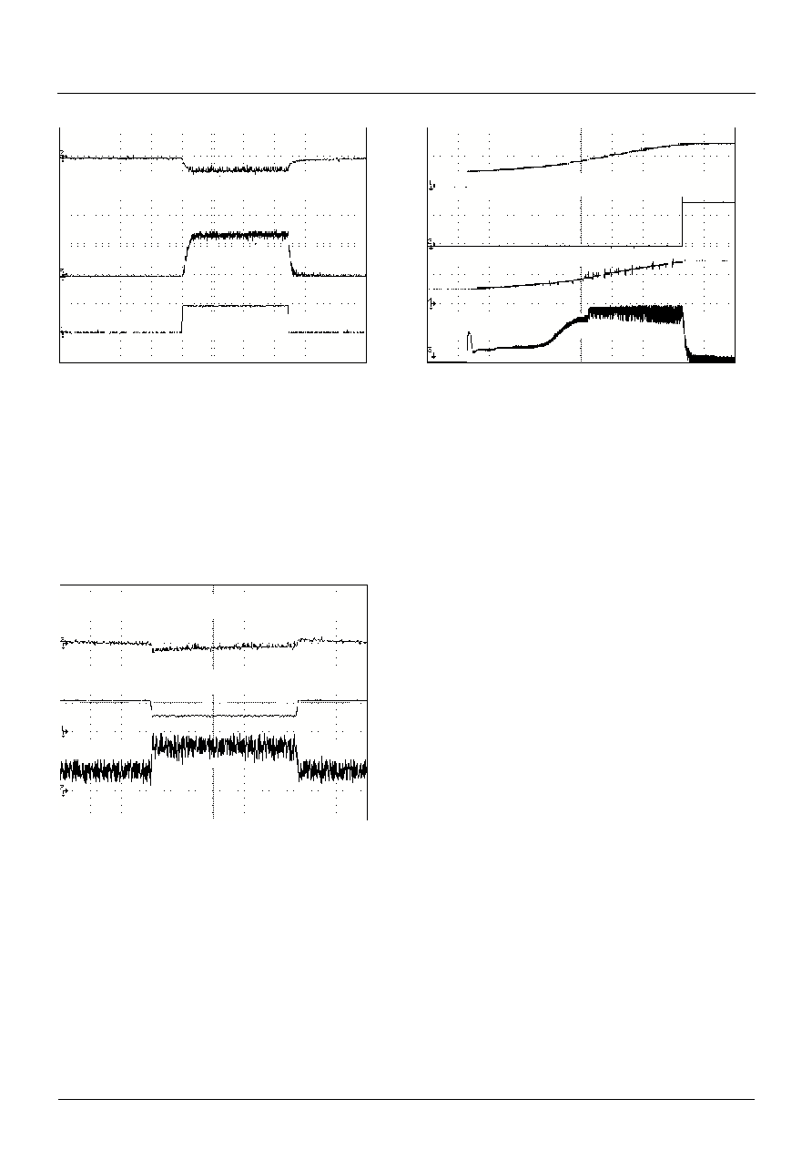
MAS 3504D
Micronas
39
Fig. 4≠22: Load Transient-Response
Fig. 4≠23: Line Transient-Response
Fig. 4≠24: Startup Waveform
500.00
µ
s/Div
V
in
= 1.2 V; V
out
= 3 V
1 Load Current
200.0 mA/Div
2 Output Voltage
100.0 mV/Div / AC-coupled
3 Inductor Current
500.0 mA/Div
3 V
0 A
0 A
I
load
= 100 mA; V
out
= 3 V
1 V
in
2.000 V/Div
2 Output Voltage
50.00 mV/Div / AC-coupled
3 Inductor Current 200.0 mA/Div
5.00 ms/Div
3 V
2 V
20
0
m
A
V
in
= 1 V; I
load
= 0 mA
1 V (DCEN)
2.000 V/Div
2 V (PUP)
2.000 V/Div
3 Inductor Current
500.0 mA/Div
4 Output Voltage
2.000 V/Div
500
µ
s/Div
0 A
3 V
3 V
3 V

All information and data contained in this data sheet are without any
commitment, are not to be considered as an offer for conclusion of a
contract, nor shall they be construed as to create any liability. Any new
issue of this data sheet invalidates previous issues. Product availability
and delivery are exclusively subject to our respective order confirmation
form; the same applies to orders based on development samples deliv-
ered. By this publication, Micronas GmbH does not assume responsibil-
ity for patent infringements or other rights of third parties which may
result from its use.
Further, Micronas GmbH reserves the right to revise this publication and
to make changes to its content, at any time, without obligation to notify
any person or entity of such revisions or changes.
No part of this publication may be reproduced, photocopied, stored on a
retrieval system, or transmitted without the express written consent of
Micronas GmbH.
MAS 3504D
40
Micronas
Micronas GmbH
Hans-Bunte-Strasse 19
D-79108 Freiburg (Germany)
P.O. Box 840
D-79008 Freiburg (Germany)
Tel. +49-761-517-0
Fax +49-761-517-2174
E-mail: docservice@micronas.com
Internet: www.micronas.com
Printed in Germany
Order No. 6251-522-1DS
5. Data Sheet History
1. Final data sheet: "MAS 3504D G.729 Annex A
Voice Codec", Nov. 7, 2001, 6251-522-1DS.
First release of the final data sheet.