 | –≠–ª–µ–∫—Ç—Ä–æ–Ω–Ω—ã–π –∫–æ–º–ø–æ–Ω–µ–Ω—Ç: MAS3506D | –°–∫–∞—á–∞—Ç—å:  PDF PDF  ZIP ZIP |
MAS 3506D
WorldSpace
Broadcast Channel
Edition July 25, 2001
6251-433-1PD
PRELIMINARY DATA SHEET
MICRONAS
MICRONAS
Audio Decoder

MAS 3506D
PRELIMINARY DATA SHEET
2
Micronas
Contents
Page
Section
Title
4
1.
Introduction
4
1.1.
Features of the MAS 3506D
4
1.2.
System Overview
7
2.
Functional Description of the MAS 3506D
7
2.1.
Overview
7
2.2.
Firmware (Internal Program ROM)
7
2.2.1.
Broadcast Channel Synchronization
8
2.2.1.1.
Broadcast Channel Timing
8
2.2.1.2.
Buffer-Controlled Loop
8
2.2.2.
Broadcast Channel Demultiplexing
8
2.2.3.
MPEG Audio Decoding
8
2.2.4.
Baseband Processing
9
2.3.
Clock Management
9
2.4.
Power Supply Concept
9
2.4.1.
Internal Voltage Monitor
9
2.4.2.
DC/DC Converter
9
2.4.3.
Stand-by Functions
9
2.4.4.
Start-up Sequence
10
2.5.
Interfaces
10
2.5.1.
Broadcast Channel (BC) Input Interface
11
2.5.2.
Parallel Input Output Interface (PIO)
12
2.5.3.
Audio Output Interface
13
3.
Controlling
13
3.1.
I
2
C-Access
13
3.1.1.
Device Address
13
3.1.2.
I
2
C Registers and Subaddresses
13
3.1.3.
Conventions for the Command Description
14
3.2.
I
2
C Control Register (Subaddress 6A
hex
)
15
3.3.
I
2
C-Data Register (Subaddresses 68
hex
and 69
hex
)
and the MAS 3506D DSP-Command Syntax
16
3.3.1.
Data Formats
16
3.3.2.
Run and Freeze (Codes 0
hex
to 1
hex
)
16
3.3.3.
Select Service Component (Code 5
hex
)
16
3.3.4.
Read Ancillary MPEG Data (Code 6
hex
)
18
3.3.5.
Read SCH-Data (Code 8
hex
)
18
3.3.6.
Write Register (Code 9
hex
)
19
3.3.7.
Write Memory (Codes A
hex
and B
hex
)
19
3.3.8.
Read Register (Code D
hex
)
19
3.3.9.
Read Memory (Codes E
hex
and F
hex
)
19
3.3.10.
Default Read
20
3.4.
Control Registers
23
3.5.
Control and Status Memory
28
3.5.1.
Volume Matrix

Contents, continued
Page
Section
Title
PRELIMINARY DATA SHEET
MAS 3506D
Micronas
3
30
4.
Specifications
30
4.1.
Outline Dimensions
31
4.2.
Pin Connections and Short Descriptions
33
4.3.
Pin Descriptions
33
4.3.1.
Power Supply Pins
33
4.3.2.
DC/DC Converter Pins
33
4.3.3.
Control Lines
33
4.3.4.
Parallel Interface Control Lines
33
4.3.5.
Parallel Interface Data Lines
34
4.3.6.
Voltage Supervision And Other Functions
34
4.3.7.
Serial Input Interface
35
4.3.8.
Serial Output Interface
35
4.3.9.
Miscellaneous
35
4.4.
Pin Configuration
36
4.5.
Internal Pin Circuits
37
4.6.
Electrical Characteristics
37
4.6.1.
Absolute Maximum Ratings
37
4.6.2.
Recommended Operating Conditions
39
4.6.3.
Characteristics
40
4.6.3.1.
I
2
C Characteristics
41
4.6.3.2.
Timing of PIO-Signals
42
4.6.3.3.
I
2
S Bus Characteristics ≠ SDI
43
4.6.3.4.
I
2
S Characteristics ≠ SDO
43
4.6.3.5.
Firmware Characteristics
44
4.6.4.
DC/DC Converter Characteristics
46
4.6.5.
Typical Performance Characteristics
52
5.
Data Sheet History
MAS 3506D
PRELIMINARY DATA SHEET
4
Micronas
WorldSpace Broadcast Channel Audio Decoder
1. Introduction
The WorldSpace system is a satellite-based digital
radio service for direct-to-home transmission of digital
radio programs. The coverage areas of this service are
Africa, South America, and parts of Asia.
The MAS 3506D is the source decoder of Micronas'
StarMan chip set that is designed for the reception of
WorldSpace signals. The MAS 3506D extracts one
Service Component (SC) of an incoming digital World-
Space Broadcast Channel (BC) and decodes
MPEG 1/2/2.5 Layer 3
1)
encoded audio data con-
tained in the selected Service Component. The Ser-
vice Control Header (SCH) information from the
Broadcast Channel is accessible via the embedded
fast mode serial control interface. The MAS 3506D
provides digital audio data output in I
2
S and similar for-
mats. An embedded digital buffer-controlled loop
recovers the sampling frequency of the audio signal
and generates a synchronized 24.576 MHz clock sig-
nal which is used as an oversampling clock for D/A
converters. A block diagram of the MAS 3506D is
shown in Figure 1≠2 on page 5.
1)
MPEG 2.5 is a compatible extension of MPEG 2
audio, defined in ISO/IEC 13818-3.2 that covers
additionally very low sampling frequencies down to
8 kHz.
1.1. Features of the MAS 3506D
≠ Single-chip WorldSpace Broadcast Channel bit-
stream demultiplexer
≠ ISO MPEG 1/2/2.5 Layer 3 decoder
≠ ISO MPEG compliance tests passed
≠ Data processing by a high-performance RISC DSP
core (MASC)
≠ Download feature provides additional functionality
≠ Self-synchronized operation
≠ Output audio data delivered (in various formats) via
an I
2
S bus (SDO)
≠ Digital volume control and stereo channel mixer
≠ Automatic soft-mute function
≠ WorldSpace SCH-data output via I
2
C interface
≠ MPEG ancillary data provided via I
2
C interface
≠ Status information accessible via PIO pins or I
2
C
≠ "CRC Error", "MPEG Frame Synchronization" and
"BC-Frame-Synchronization" indicators
≠ Power management for reduced power consump-
tion at lower sampling frequencies
≠ Low power dissipation (30 mW at fs
12 kHz,
46 mW at fs
24 kHz, 86 mW at fs > 24 kHz at
2.7 V)
≠ Supply voltage range: 2.7 V to 3.6 V
≠ Adjustable built-in DC/DC up-converter for one-cell
and two-cell battery operation (typically down to
V
bat
= 0.9 V)
≠ Adjustable power supply supervision
≠ Power-off function
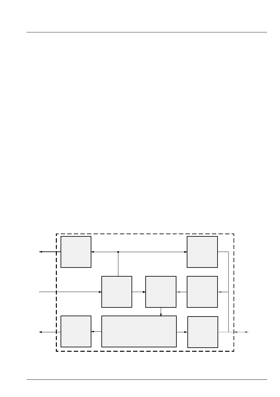
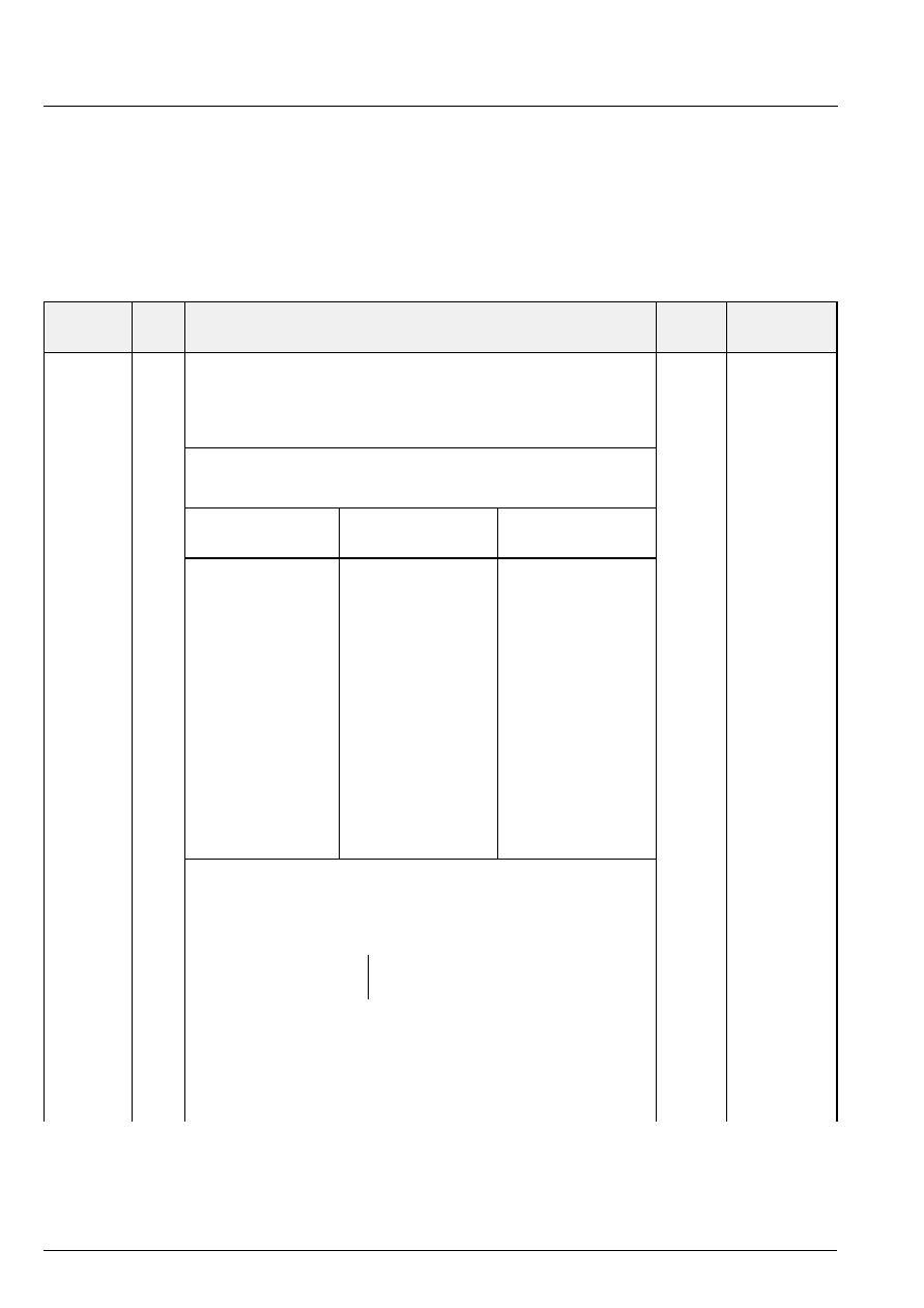
1.2. System Overview
The Micronas StarMan chip set consists of the channel
decoder DRD 3515A and the MPEG Layer 3 audio
decoder MAS 3506D. All essential analog and digital
building blocks for WorldSpace reception are provided
by the chip set. Together with an L-band tuner and an
appropriate microcontroller this set creates a complete
StarMan radio receiver (Figure 1≠1)
Fig. 1≠1: Standard application of the StarMan chip set
Since the DRD 3515A also contains an audio amplifier
for headphone or small loudspeaker operation, only a
minimum of external components is necessary. The
additional inputs for analog signals (e.g. conventional
AM/FM receiver, tape etc.) make the amplifier accessi-
ble to these audio sources and thus considerably sim-
plify the design of complete radio receivers.
The analog audio output of the WorldSpace signal can
be connected to an external stereo amplifier for higher
power or quality. Also a digital audio signal in standard
I
2
S format is provided for high-end applications that
may require an external D/A converter.
AM/FM
Receiver,
Tape Player
WorldSpace
Tuner
System
Controller
DRD 3515A
MAS 3506D
Aux1/2
(analog)
IF input
BC
I
2
S
SC-out
analog out
I
2
C
PRELIMINARY DATA SHEET
MAS 3506D
Micronas
5
The complete WorldSpace Broadcast Channel (BC) is
available as a serial output signal from the DRD 3515A
and provides full access to all WorldSpace data. The
additional Service Component (SC) output of the
DRD 3515A may be useful in applications where a
data and an audio channel are transmitted simulta-
neously. In this case, the data component is directed
to the SC output. This function is independent from the
audio Service Component extraction in the
MAS 3506D.
Service Control Header data are available via I
2
C con-
troller interface from the MAS 3506D. (N.B. The Time
Slot Control Channel data are available only from the
DRD 3515A.)
Fig. 1≠2: Block diagram of the MAS 3506D
Clock
Synthe-
sizer
Serial
Input
Interface
Serial
Output
Interface
RCLK
OCLK
14.725 MHz
24.576 MHz
BC in
Audio
Data out
to DRD
35
15A
Service Component
Extraction from Broadcast Channel
MPEG 1/2/2.5 Layer 3
Audio Decoding
Buffer-Controlled Loop
20-Bit RISC DSP
I
2
C
Interface
Parallel
Interface
DC/DC
Converter
VDD
to
µ
C
MAS
350
6D
PR
EL
I
M
IN
A
R
Y D
A
TA
SH
EE
T
6
M
i
c
r
onas
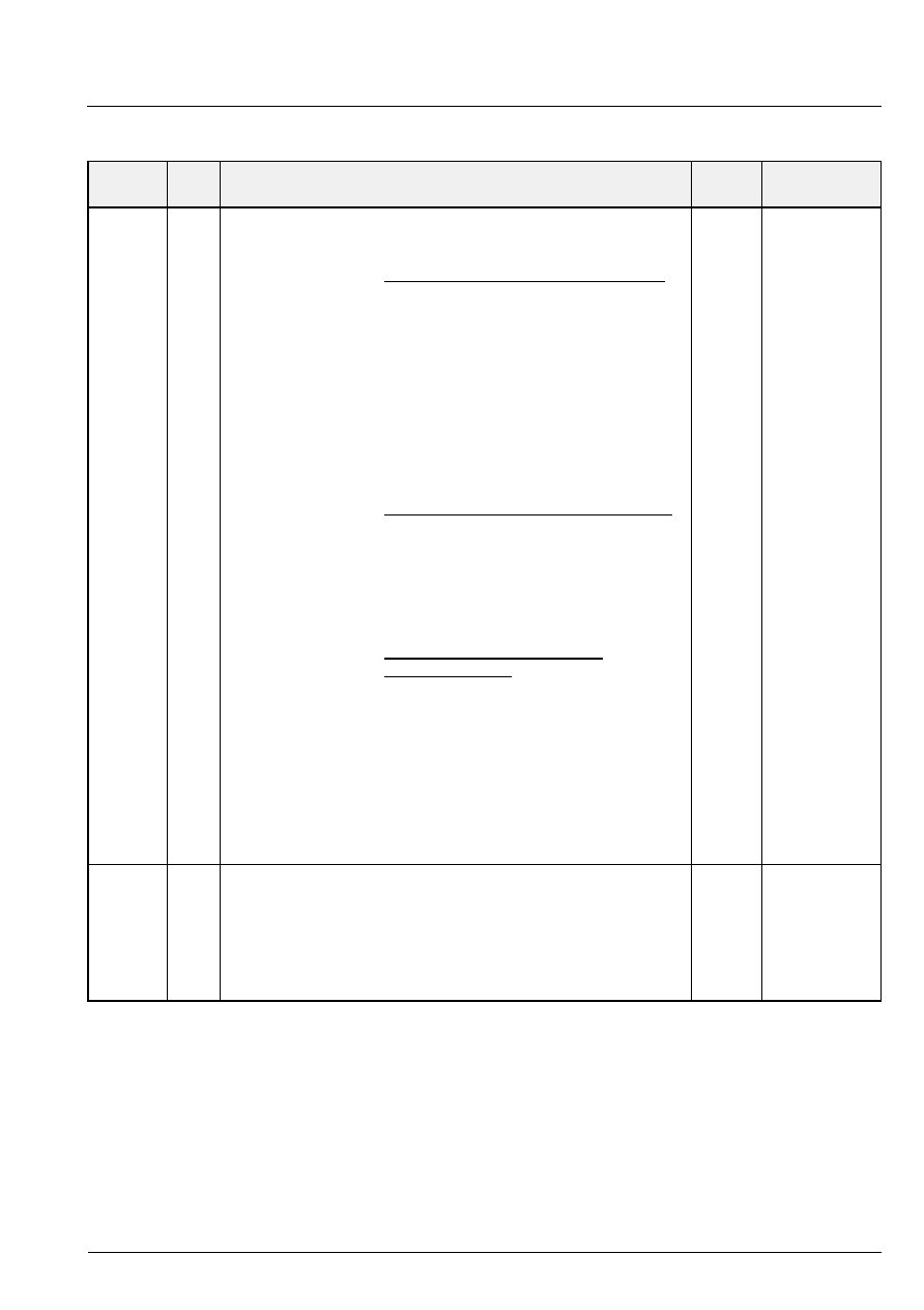
Fig. 1
≠
3:
Com
p
l
e
te
W
o
r
l
d
S
pa
ce
r
e
c
e
iv
er
b
l
oc
k
di
agr
am
Audio Out
FM/AM Demod.
DRD3515A
MAS3506D
µC
Left
Right
LCD
Mono
A
Line
Stereo
Keys
3.0 V
3
PUP
WRDY
PUP
CLKI
FM/AM
Antenna
Double Superhet
L-Band Tuner
Pol.-
Switch
Satellite
Antenna
BCDout
BCC
SCDout
SCC
To optional BC processing
To optional SC processing
SCW
BCDin
BCenable
BC data input from ext. processing
regulated Voltage (3 V)
SCI-Control Bus
DCEN
WSEN
DC/DC
Con-
verter
MPEG
Layer 3
Decoder
Buffer-
controlled
Clock
Synthesizer
QPSK Dem.
and Timing
Recovery
FEC
and TDM
Demux
D/A and
Analog Audio
4 OClk
24.576 MHz
Digital Audio
Input
Buffer
SC Extr.
Output Buffer
14.725 MHz
1
RClk
2nd IF
2
C
B
PRELIMINARY DATA SHEET
MAS 3506D
Micronas
7
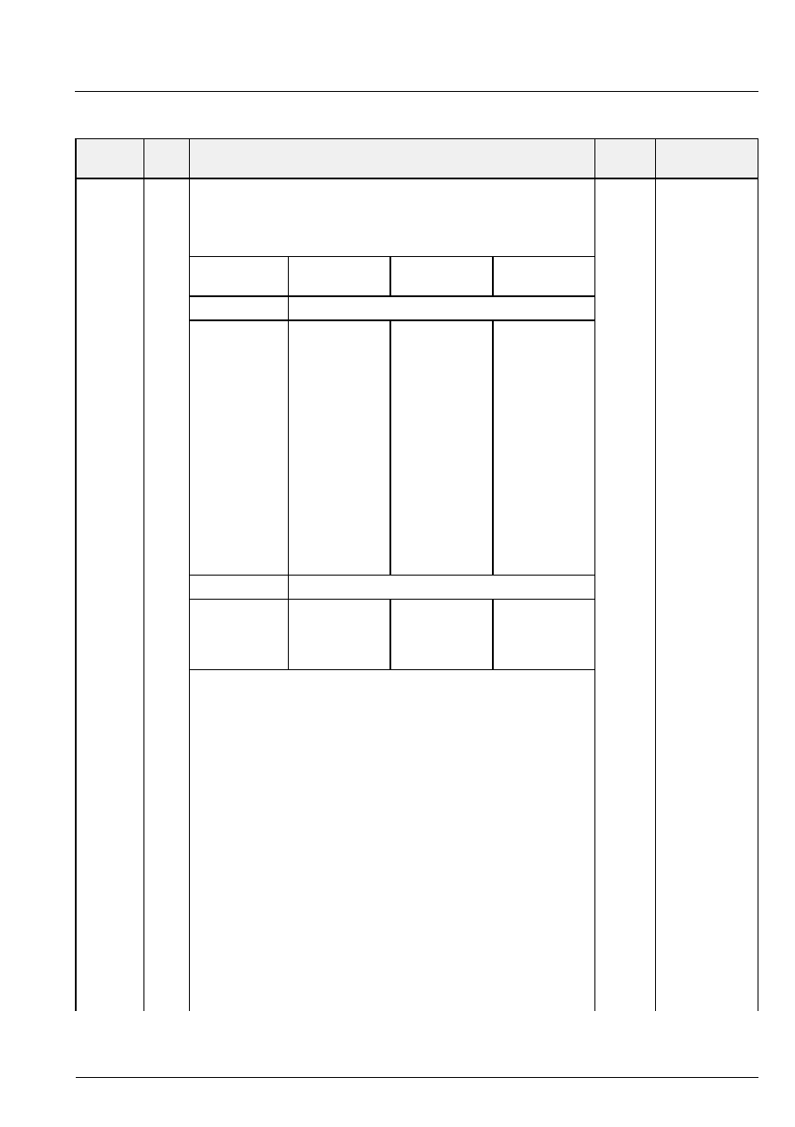
2. Functional Description of the MAS 3506D
2.1. Overview
The hardware of the MAS 3506D consists of a high-
performance RISC Digital Signal Processor (DSP) and
appropriate interfaces for WorldSpace Broadcast
Channel decoding (see Figure 2≠1). The internal pro-
cessor works with a memory word length of 20 bits and
an extended range of 32 bits in its accumulators. The
instruction set of the DSP is highly optimized for audio
data compression and decompression. Thus, only very
small areas of internal RAM and ROM are required. All
the data input and output actions are based on a 'non-
cycle-stealing' background DMA that does not cause
any computational overhead (except for some initial-
ization). The overall function of the MAS 3506D can be
altered by downloading up to 1 kWord of program
code into the internal RAM and executing this code
instead of the built-in firmware ROM code
1)
. Dedicated
clock management hardware supports synchronization
on the transmitted data signal. A DC/DC step-up con-
verter has been integrated for efficient battery-based
operation. Fig. 2≠1 shows the building blocks of the
MAS 3506D.
1)
Detailed information about downloading is provided
in combination with the MAS 3506D software devel-
opment package or together with the MAS 3506D
software modules available from Micronas.
2.2. Firmware (Internal Program ROM)
The firmware of the MAS 3506D operates on the
Broadcast Channel signal generated by the
DRD 3515A. The MAS 3506D firmware processes the
input signal in four steps.
≠ Broadcast Channel synchronization
≠ Broadcast Channel demultiplexing
≠ MPEG audio decoding
≠ Frame synchronization and decoding error signals
are provided at output pins of the MAS 3506D.
2.2.1. Broadcast Channel Synchronization
The MAS 3506D analyzes the incoming BC bitstream
and detects the Service Control Header (SCH) pream-
ble. If the preamble is found, the BC-SYNC signal
(available at a MAS 3506D output pin) indicates that
the MAS 3506D is in synchronized state. If synchroni-
zation is lost, the MAS 3506D automatically resets the
BC-SYNC signal and performs an audio soft-mute until
the next SC-header is detected.
Fig. 2≠1: Functional overview of the MAS 3506D
OCLK
BC input
Digital Audio
output
Clock
Synthesizer
Volume
Matrix
SCH
buffer
Configuration
Registers
SCH
Synchro-
Service
Component
Selection
Layer 3
Status
Data Buffer
Ancillary
Data
MPEG 1/2/2.5 Layer 3
Decoder
nization
to
µ
C
(I
2
C)
to
DRD
3
515
A

MAS 3506D
PRELIMINARY DATA SHEET
8
Micronas
2.2.1.1. Broadcast Channel Timing
The incoming Broadcast Channel bitstream has a
framing with a period between Prime Rate Channel
Preambles (PRCP) of
prcpt = 432 ms
During one frame the transmission of the BC is inter-
rupted by a gap prcpgap of:
prcpgap = 2.5 ms
The data transmission is interrupted by a second gap
mfpgap with a duration of
mfpgap = 1.2 ms
that is synchronous with the Master Frame Preamble
(MFP) cycle with a period of:
mfpt = 138 ms
Both cycles mfpt and prcpt have a least common multi-
ple at 9936 ms. These gaps are independent of the
number of Prime Rate Channels (PRC) n that create
the considered Broadcast Channel.
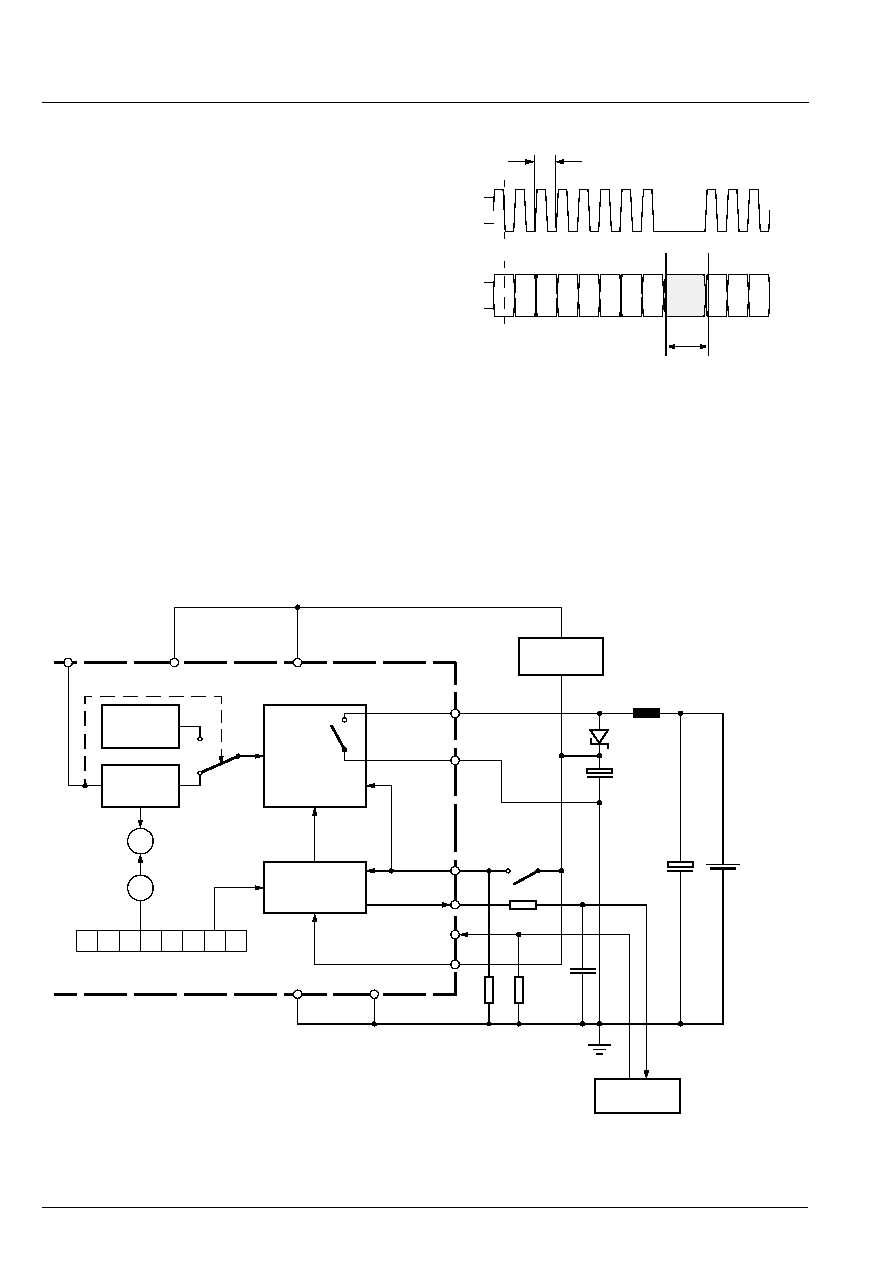
2.2.1.2. Buffer-Controlled Loop
For the recovery of the audio sample clock, a buffer-
controlled loop is used that operates on the incoming
Broadcast Channel bit stream. The buffer control loop
characteristic suppresses the effects of these gaps on
the stability of the generated audio sample frequency
by more than 40 dB. Thus, no audible jitter is intro-
duced to the derived reference clock for the D/A con-
verter (see section 2.3. "Clock Management").
The step response of the buffer-controlled loop is plot-
ted in Figure 2≠2 with respect to different number of
PRCs. The settling time for the buffer-controlled loop is
about 10 s.
Fig. 2≠2: buffer-controlled loop step response
2.2.2. Broadcast Channel Demultiplexing
The Service Control Header that directly follows the
SCH-preamble in the BC bitstream is made accessible
to the controller after it has been detected. Its availabil-
ity is indicated by the BC-FRAME-SYNC signal. Infor-
mation about the content of the Broadcast Channel is
given in the Service Control Header data. The control-
ler may select the number of the Service Component
that is to be passed to the internal MPEG audio
decoder. By default, always Service Component "0" is
decoded by the MAS 3506D. An implemented
autoscan mode can be selected that skips non-audio
Service Components.
2.2.3. MPEG Audio Decoding
The MPEG 1/2/2.5 Layer 3 decoder performs the
audio decoding. The steps for decoding are:
≠ Synchronization
≠ Side information extraction
≠ Huffman decoding
≠ Synthesis filter bank
≠ Ancillary data extraction
The bit rates and sampling rates that are supported by
the MAS 3506D are listed in Table 2≠1.
Frame synchronization and decoding error signals are
provided at output pins of the MAS 3506D.
2.2.4. Baseband Processing
A digital volume control matrix is applied to the digital
stereo audio data. This matrix may also perform addi-
tional balance control and a simple kind of stereo
basewidth enhancement. The four factors LL, LR, RL,
and, RR are adjustable via the controller with 20 bit
resolution (see Fig. 3≠2 on page 28).
4.3
8.6
13
17
21
0.02
0.04
0.06
0.08
0.1
0.12
t/s
Table 2≠1: Sampling frequencies and bit rates
Sampling Freq. in kHz
Bit rates in kBit/s
48, 32, 24, 16, 12, 8
128, 112, 96, 80, 64, 56,
48, 40, 32, 24, 16, 8
PRELIMINARY DATA SHEET
MAS 3506D
Micronas
9
2.3. Clock Management
The complete StarMan chip set is driven by a single
crystal with a nominal frequency of 14.725 MHz.
The DRD 3515A contains the crystal oscillator and an
appropriate clock buffer to generate the clock signal
RClk. This RClk signal is used as reference clock for
the MAS 3506D by an internal clock synthesizer that
generates an internal system clock of 24.576 MHz.
This synchronized clock frequency is passed back to
the DRD 3515A for use in its embedded audio D/A
converter.
2.4. Power Supply Concept
The MAS 3506D offers an embedded controlled DC/
DC converter for battery based power supply con-
cepts. It works as an up-converter.
2.4.1. Internal Voltage Monitor
An internal voltage monitor compares the input voltage
at the VSENS pin with an internal reference value that
is adjustable via I
2
C bus. The PUP output pin should
be observed by the controller. It becomes inactive
when the voltage at the VSENS pin drops below the
programmed value of the reference voltage.
It is important that the WSEN must not be activated
before the PUP signal is generated. The PUP signal
thresholds are listed in Table 3≠10 on page 20. The
internal voltage monitor will be activated with a high
level at Pin DCEN.
2.4.2. DC/DC Converter
The DC/DC converter of the MAS 3506D is used to
generate a fixed power supply voltage even if the chip
set is powered by battery cells in portable applications.
The DC/DC converter is designed for the application of
1 or 2 batteries or NiCd cells as shown in Fig. 2≠5
which shows the standard application circuit. The DC/
DC converter is switched on by activating the DCEN
pin. Its output power is sufficient for supplying the com-
plete radio receiver.
Note: Connecting DCEN directly to VDD leads to
unexpected states of the DCCF register.
A 22
µ
H inductor is required for the application. The
important specification item is the inductor saturation
current rating, which should be greater than 2.5 times
the DC load current. The DC resistance of the inductor
is important for efficiency. The primary criterion for
selecting the output filter capacitor is low equivalent
series resistance (ESR), as the product of the inductor
current variation and the ESR determines the high-fre-
quency amplitude seen on the output voltage. The
Schottky diode should have a low voltage drop V
D
for
a high overall efficiency of the DC/DC converter. The
current rating of the diode should also be greater than
2.5 times the DC output current. The VSENS pin has
to be always connected to the output voltage.
2.4.3. Stand-by Functions
A high level at pin WSEN enables both, the DSP
including the I
2
C-block and the DC/DC-converter. If
the DSP-functions (audio decoding) are not needed,
the DC/DC-converter may remain active to supply
other parts of the radio. This mode is entered by set-
ting DCEN to "high" and WSEN to "low". No I
2
C control
is possible in this mode.
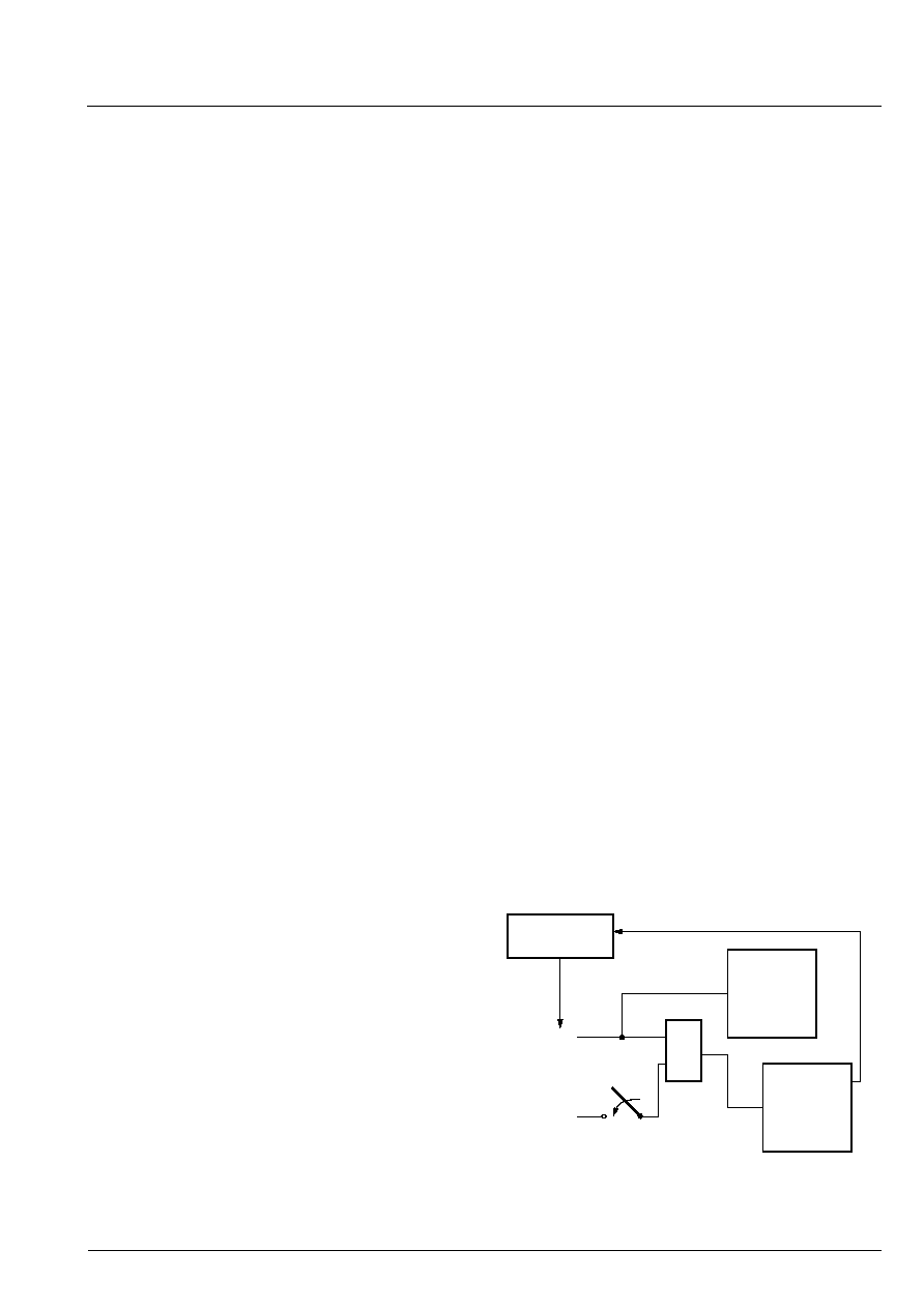
2.4.4. Start-up Sequence
The DC/DC converter starts from a minimum input
voltage of 0.9 V. There should be no output load dur-
ing startup. WSEN must be "low". The start-up script
should be as follows:
1. Start the DC/DC-converter with a high signal (VDD,
AVDD) at pin DCEN.
2. Wait until PUP goes "high".
3. It is recommended to wait at least one millisecond to
guarantee that the output voltage has settled.
4. The controller may now enable the DSP with a
"high" signal at pin "WSEN".
Please also refer to Figure 2≠3.
Fig. 2≠3: DC/DC operation
> 0.9 V
WSEN > 2 V
DCEN
1
DSP
operation
µController
DC/DC
On
button
MAS 3506D
PRELIMINARY DATA SHEET
10
Micronas
2.5. Interfaces
The MAS 3506D uses an I
2
C control interface, a serial
input interface for the Broadcast Channel, and a digital
audio output interface for the decoded audio data (I
2
S
or similar). Additionally, a general-purpose parallel I/O
interface (PIO) may be used for monitoring and mode-
selection tasks. The PIO lines are controlled by the
internal firmware.
2.5.1. Broadcast Channel (BC) Input Interface
The BC input interface consists of the three pins SIC,
SII, and SID. For WorldSpace operation the SII pin is
always to be connected to VSS. The Broadcast Chan-
nel input signal format is shown in Figure 2≠4. The
data values are latched with the falling edge of the SIC
signal. The input interface is asynchronous and
accepts data streams generated by the DRD 3515A
BC output.
Fig. 2≠4: Schematic timing of the SDI (BC) input
The BC input can be switched to an alternate port.
This function is controlled by input pin PI18. For more
details please see Section 3.1.3. on page 13
L
Fig. 2≠5: DC/DC converter connections
7 6 5 4 3 2 1 0
t
SICLK
l
t
bw
BCC
(SIC)
BCD
(SID)
V
h
V
I
V
h
V
I
0...15
32...47
64...94
10
16
-
+
-
+
VSS
AVSS
AVDD
VDD
CLKI
DCSO
DCSG
DCEN
PUP
WSEN
VSENSE
9
47 k
47 k
Power-On
Push Button
10 k
10 nF
DC/DC
converter
voltage
monitor
Start-up
oscillator
µ
Controller
22
µ
H
V
IN
0.9 V
C
OUT
330
µ
F
Low ESR
C
IN
330
µ
F
DCCF
8e
hex
optional
filter
Start-up
oscillator
+32
x2
PRELIMINARY DATA SHEET
MAS 3506D
Micronas
11
2.5.2. Parallel Input Output Interface (PIO)
The parallel interface of the MAS 3506D consists of
the lines PI0..PI4, PI8, PI12..PI19:
These signals are used to indicate the status of the
Broadcast Channel and the MPEG Layer 3 decoder.
The PIO pin status is also accessible via I
2
C interface
(see Table 3≠10).
Table 2≠2: PIO input and output pin assignment
during MPEG decoding
PIO
Pin
Name
Comment
PI19
(O)
BC-FRAME-TOGGLE
0
1
Output level tog-
gled each BC-
FRAME
PI18
(I)
BCINENABLE
0
1
enables SI* inputs
enables SI inputs
PI13
(O)
BC-FRAME-SYNC
0
1
start of new frame
P12
(O)
BC-SYNC
0
1
unsynched
synched to BC
PI8
(O)
MPEG-CRC-ERROR
0
1
no error
CRC-error or sync
lost
PI4
(O)
MPEG-FRAME-SYNC
0
1
sync to a new
MPEG frame
PI3
(I)
AUD-SW
May be used to
monitor a signal
indicating switch-
ing between
Headphone and
Loudspeaker
mode.
PI2,
PI1,
PI0
(I)
Reserved
The PI-pins may
be monitored by
reading the PIO
register (see
Table 3≠10)
MAS 3506D
PRELIMINARY DATA SHEET
12
Micronas
2.5.3. Audio Output Interface
The audio output interface of the MAS 3506D is a
standard serial audio interface. The interface is config-
urable by software to work in 16-bit/sample and 32-bit/
sample mode. The default setup is a 16-bit mode
which is also the default setting for the DRD 3515A.
The 32-bit/sample mode is provided for high-resolution
D/A converters that expect more than 16-bit/sample
input data. The embedded D/A-converter of the
DRD 3515A is also capable of decoding the 32-bit/
sample format and provides a slightly better S/N per-
formance in this mode
1)
. The audio output interface
timing is shown in Figure 2≠6 and Figure 2≠7.
1)
If the 32-bit mode is selected and the D/A converter
of the DRD 3515A is still connected, it also has to
be switched to 32-bit I
2
S mode.
Fig. 2≠6: Schematic timing of the digital audio output interface in 16-bit/sample mode
Fig. 2≠7: Schematic timing of the digital audio output interface in 32-bit/sample mode
DAD
V
h
V
l
15 14 13 12 11 10 9 8 7 6 5 4 3 2 1 0 15 14 13 12 11 10 9 8 7 6 5 4 3 2 1 0
left 16-bit audio sample
right 16-bit audio sample
0
timing detail
V
h
V
l
DAI
15
DAI
DAD
DAD
V
h
V
l
left 32-bit audio sample
right 32-bit audio sample
0
timing detail
V
h
V
l
DAI
1
31
0
31
0
31
PRELIMINARY DATA SHEET
MAS 3506D
Micronas
13
3. Controlling
3.1. I
2
C-Access
Communication between the MAS 3506D and the
external controller is done via an I
2
C slave interface.
3.1.1. Device Address
The device addresses are 3a
hex
for writing (DW) and
3b
hex
for reading (DR), respectively. I
2
C clock syn-
chronization is used to slow down the bus if required.
3.1.2. I
2
C Registers and Subaddresses
The interface uses one level of subaddresses. The
MAS 3506D interface has 3 subaddresses allocated
for the corresponding I
2
C-registers.
The address 6a
hex
is used for basic control, i.e. reset
and task select. The other addresses are used for data
transfer from/to the MAS 3506D.
The I
2
C-control and data registers of the MAS 3506D
are 16 bits wide, the MSB is denoted as bit [15]. Trans-
missions via I
2
C-bus have to take place in 16-bit words
(two byte transfers, MSB sent first); thus for each reg-
ister access two 8-bit data words must be sent/
received via I
2
C-bus.
3.1.3. Conventions for the Command Description
The description of the various controller commands
uses the following formalism:
≠ Abbreviations used in the following descriptions:
a
address
d
data value
n
count value
o
offset value
r
register number
x
don't care
≠ Memory addresses like D1:89f are always in hexa-
decimal notation.
≠ A data value is split into 4-bit nibbles which are
numbered beginning with 0 for the least significant
nibble.
≠ Data values in nibbles are always shown in hexa-
decimal notation.
≠ A hexadecimal 20-bit number d is written, e.g. as
d = 17c63
hex
, its five nibbles are
d0 = 3
hex
, d1 = 6
hex
, d2 = c
hex
, d3 = 7
hex
, and d4 =
1
hex
.
≠ Variables used in the following descriptions:
DW
3a
hex
I
2
C-device write
DR
3b
hex
I
2
C-device read
data_write
68
hex
data register write
data_read
69
hex
data register read
control
6a
hex
control register write
≠ Bus signals
S
Start
P
Stop
A
ACK = Acknowledge
N
NAK = Not acknowledge
W Wait = a wait time (
4 ms) may occur
≠ Symbols in the telegram examples
<
Start condition
>
Stop
dd
data byte
xx
ignore
All telegram digits are hexadecimal, data originating
from the MAS 3506D are grayed.
Example:
<3a 68 dd dd>
write data to DSP
<3a 69 <3b
dd dd
>
read data from DSP
Figure 3≠1 shows I
2
C bus protocols for read and write
operations of the interface; the read operation requires
an extra start condition and repetition of the I
2
C-device
address with the read command (DR). Fields with sig-
nals/data originating from the MAS 3506D are marked
by a gray background. Note that in some cases the
data reading process must be concluded by a NAK
condition.
The MAS 3506D firmware scans the I
2
C interface peri-
odically and checks for pending or new commands.
Table 3≠1: I
2
C device address bits
A6
A5
A4
A3
A2
A1
A0
write/
read
0
0
1
1
1
0
1
0/1
Table 3≠2: I
2
C subaddresses
Sub-
address
I
2
C-
Register
Function
68
hex
data_write
Controller writes to
MAS 3506D data register
69
hex
data_read
Controller reads from
MAS 3506D data register
6a
hex
control
Controller writes to
MAS 3506D control register
MAS 3506D
PRELIMINARY DATA SHEET
14
Micronas
The commands are then executed by the DSP during
its normal operation without any loss or interruption of
the incoming data or outgoing audio data stream.
However, due to some time critical firmware parts, a
certain latency time for the response has to be
expected at the locations marked with a "W" (= wait).
The theoretical worst case response time does not
exceed 4 ms. However, the typical response time is
less than 0.5 ms.
3.2. I
2
C Control Register (Subaddress 6A
hex
)
The I
2
C control register is a write-only register. Its
main purpose is the software reset of the MAS 3506D.
The software reset is done by writing a 16-bit word to
the MAS 3506D with bit 8 set. The 4 least significant
bits are reserved for task selection. The task selection
is only useful in combination with download software.
In the standard application these bits must always be
set to 0.
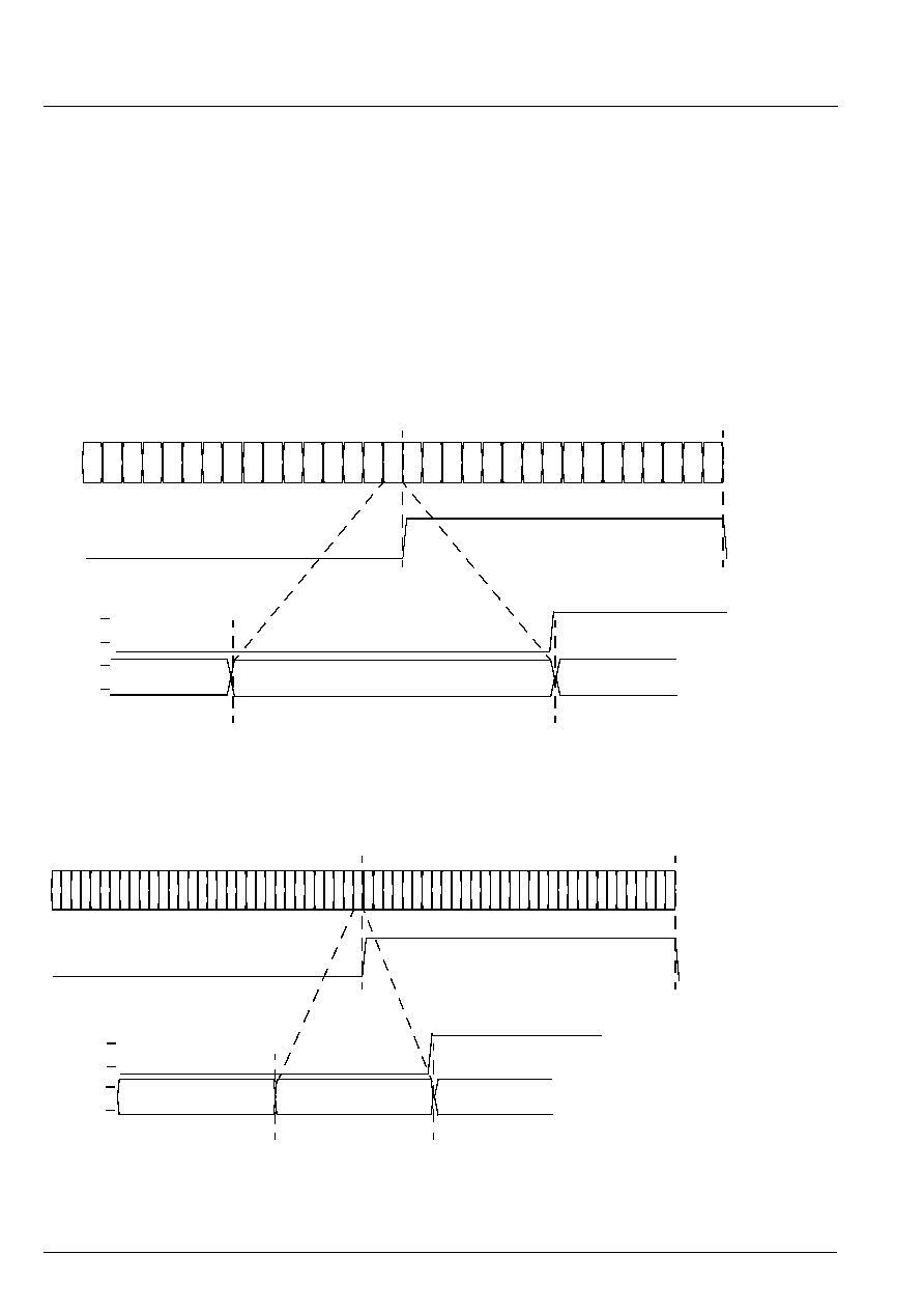
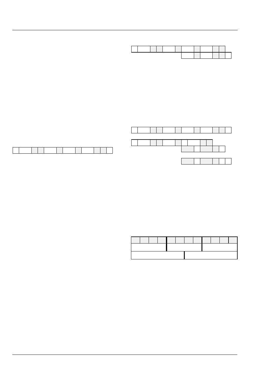
Fig. 3≠1: I
2
C-bus protocol for the MAS 3506D. Signals originating from the MAS 3506D are grayed.
Table 3≠3: Control register data bit assignment
1)
1) x = don't care, R = reset, T3...T0 = task selection
15 14 13 12 11 10 09 08 07 06 05 04 03 02 01 00
x
x
x
x
x
x
x
R
0
0
0
0
T3 T2 T1 T0
S
DW
control
W
A
A
A
W
A
P
d3,d2
d1,d0
W
high byte data
low byte data
A
P
Example: I
2
C write access
SDA
SCL
1
0
S
P
DR (3b
hex
)
Example: I
2
C read access
DW (3a
hex
)
data_read (69
hex
)
S
DW (3a
hex
)
A
data_write (68
hex
)
A
high byte data
A
low byte data
A
P
N
W = Wait
A = Acknowledge (Ack)
N = Not Acknowledge (NAK)
S = Start
P = Stop
A
S
S
A
A
A
W
W
W
W
PRELIMINARY DATA SHEET
MAS 3506D
Micronas
15
3.3. I
2
C-Data Register (Subaddresses 68
hex
and
69
hex
) and the MAS 3506D DSP-Command
Syntax
The I
2
C data register is used to communicate with the
internal firmware of the MAS 3506D. It is readable
(subaddress "data_read") and writable (subaddress
"data_write") and also has a length of 16 bits. The data
transfer is done with the most significant bit (m) first.
A special command language is used that allows the
controller to access the DSP-registers and RAM-cells
and thus monitor internal states, set the parameters for
the DSP-firmware, control the hardware, and even pro-
vide a download of alternative software modules. The
DSP-commands consist of a "Code" which is sent to to
I
2
C-data register together with additional parameters.
Table 3≠5 gives an overview over the different com-
mands which the DSP-core may receive. The "Code"
is always the first data nibble transmitted after the
"data_write" byte.
The control interface is also used for low-bit-rate data
transmission, i.e. MPEG-embedded ancillary data and
the WorldSpace Service Control Header. These data
are available in a specified memory area of the
MAS 3506D after successful decoding. The synchroni-
zation between controller and the MAS 3506D will be
done by observing the BC-FRAME-SYNC and MPEG-
FRAME-SYNC signals in register c8
hex
or at the corre-
sponding pins.
Table 3≠4: Data register bit assignment
15 14 13 12 11 10 09 08 07 06 05 04 03 02 01 00
m
l
...
S
DW
data_write
W
A
A
A
A
Code,...
...,...
Table 3≠5: Basic controller command codes for the MAS 3506D
Code
(hex)
Command
Function
0
Run
Start execution of an internal program. Run with start address 0
hex
means
freeze the operating system
1
Run Config
Start execution of an internal program and switch config RAM to P-RAM
5
Select SC
Select the Service Component
6
Read Ancillary Data
Read MPEG ancillary data
8
Read SCH-Data
Read Service Control Header
9
Write Register
An internal register of the MAS 3506D can directly be written to by the con-
troller
a, b
Write Memory
A block of the DSP memory can be written to by the controller. (This feature
may be used to download alternate programs.)
d
Read Register
The controller can read an internal register of the MAS 3506D
e, f
Read Memory
A block of the DSP memory can be read by the controller
MAS 3506D
PRELIMINARY DATA SHEET
16
Micronas
3.3.1. Data Formats
The internal data word size is 20 bits. All RAM-
addresses can be accessed in a 20-bit mode via I
2
C-
bus. Because of the 16-bit width of the I
2
C-data regis-
ter the full transfer of all 20 bits requires two 16-bit I
2
C-
words. Some commands only access the lower 16 bits
of a cell. For fast access of internal DSP-states the
processor core also has an address space of 256 data
registers.
The internal data format is a 20 bit two's complement
denoted "r". If in some cases a fixed point notation "v"
is necessary. The conversion between the two forms
of notation is done as follows:
r = v*524288.0+0.5; (
-
1.0
v < 1.0)
v = r/524288.0; (
-
524288 < r < 524287)
3.3.2. Run and Freeze (Codes 0
hex
to 1
hex
)
The Run command causes the start of a program part
at address a = (a3,a2,a1,a0). Note that nibble a3 is
also the command code (see Table 3≠5) and thus it is
restricted to certain values. This command is espe-
cially used to start alternate code or downloaded code
from a RAM-area that has been configured as program
RAM.
Example 1: Start program execution at address
345
hex
:
<3a 68 03 45>
Freeze is a special run command with start address 0.
It suspends all normal program execution. The operat-
ing system will enter an idle loop so that all registers
and memory cells can be watched. This state is useful
for operations like downloading code or contents of
memory cells because the internal program cannot
overwrite these values. This freezing will be required if
alternative software is downloaded into the internal
RAM of the MAS 3506D.
Freeze has the following I
2
C protocol:
<3a 68 00 00>
The entry point of the default software will be accessed
automatically after a reset, thus issuing a Run or
Freeze command is only necessary for starting down-
loaded software or special program modules which are
not part of the standard set.
3.3.3. Select Service Component (Code 5
hex
)
Select the (zero-based) service component with the
number d = d0. The number of available service com-
ponents is to be taken from the SCH information. A
maximum of 8 service components are allowed in one
Broadcast Channel. SC-selection is also possible by
writing to memory cell D1:7ef (see Table 3≠11 on
page 23).
3.3.4. Read Ancillary MPEG Data (Code 6
hex
)
The availability of new ancillary data is indicated by the
MPEG-FRAME-SYNC signal in register c8
hex
or at the
corresponding pin. Ancillary data are available every
24 to 32 ms depending on the sample rate of the
MPEG-bitstream. The instruction parameters are
embedded in the 3 nibbles o2..o0. The 6 MSBs indi-
cate the address offset counted in 16-bit words where
the read-out of the ancillary data shall start. The 6
LSBs indicate the number of 16-bit words that are to
be transmitted by MAS 3506D.
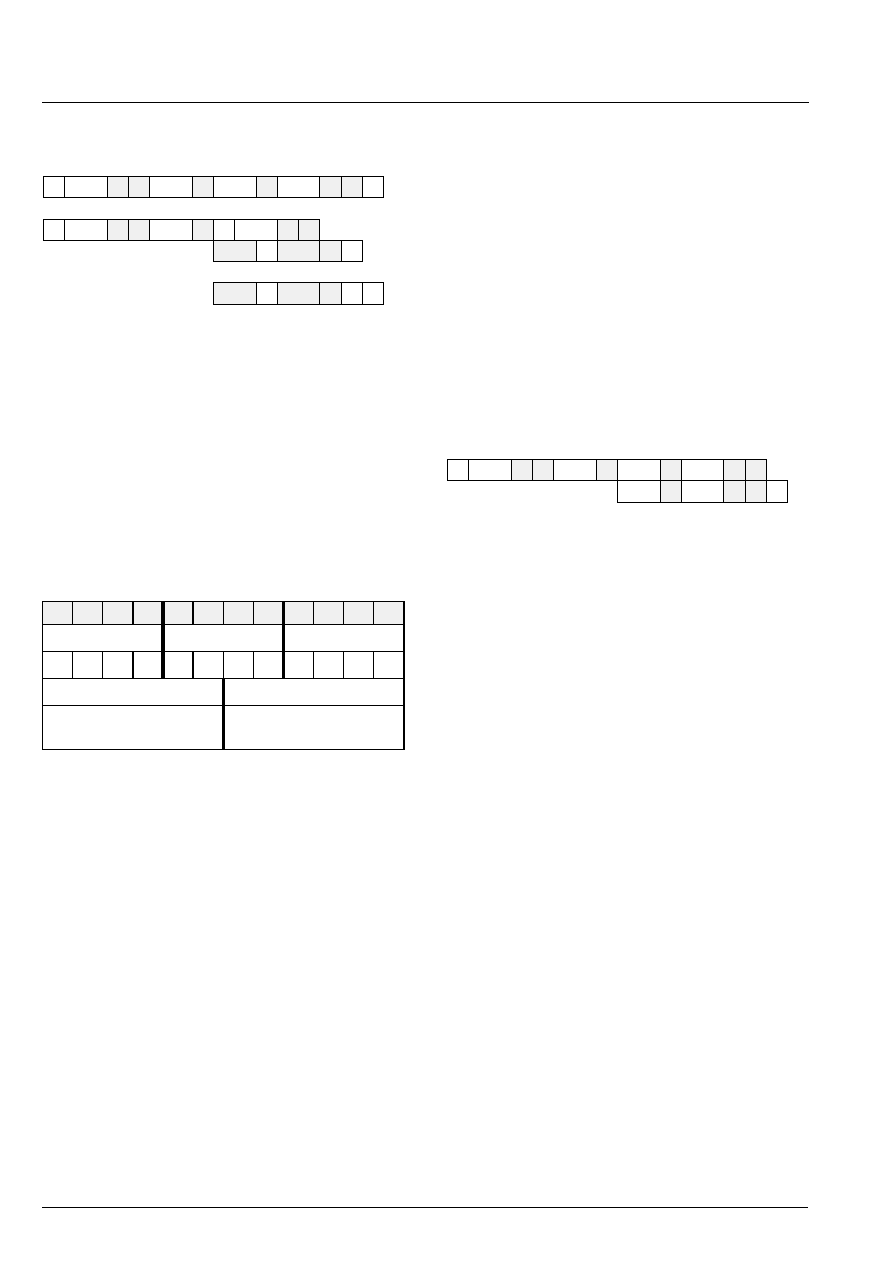
S
DW
data_write
W
A
A
A
W
A
P
a3,a2
a1,a0
Table 3≠6: Arrangement of o-bits
11
10
9
8
7
6
5
4
3
2
1
0
o2
o1
o0
address offset
number of 16-bit words
S
DW
data_write
W
A
A
A
W
A
5,0
0,0
P
A
W
A
0,0
0,d0
1) send command (Read D0)
2) get ancillary data values
S
DW
data_write
W
A
A
A
W
A
6,o2
o1,o0
S
DW
data_read
W
A
A
S
A
DR
P
P
W
A
d3,d2
A
d1,d0
N
W
d3,d2
A
d1,d0
....repeat for n data values....
W
PRELIMINARY DATA SHEET
MAS 3506D
Micronas
17
The data values that are returned are organized in the
following table:
The ancillary data values are copied in the reverse
order into this data field where the last bit received is
place at bit 0 of the data word at offset 3. The number
of data words with content can be calculated as fol-
lows:
int [(NumberOfAncillaryBits-1)/16] + 1
Limitations:
≠ The maximum number of data words that can be
read out are 28.
≠ The upper limit for ancillary data bitrate is 9600 bps.
≠ The ancillary data are only valid for 6 ms after the
MPEG-FRAME-SYNC signal.
Memory example:
The MPEG bitstream contains 20 bits of ancillary data
with the content f0f08
hex
. Then the ancillary data field
content will be:
Telegram example:
First get the content of 'Number of ancillary bits':
<3a
device write ( I
2
C-address)
68
data write
60 81>
code 6
hex
, offset 2, count 1:
Get number of ancillary bits
<3a 69 <3b
initiate reading
dd dd
>
and read number of bits
Calculate number of words to be read from the number
of bits received (e.g. 20 bits require two words).
<3a
device write (I
2
C-address)
68
data write
60 c2>
code 6
hex
, offset 3, count 2:
Read two words from offset 3.
<3a 69 <3b
initiate reading
dd dd
and read two words
dd dd
>
Table 3≠7: Content of ancillary data field
Offset
Content
0
Bit 17..32 of MPEG header
1)
1) see address D1:7f6 in Table 3≠11 on page 23
1
Bit 12..16 of MPEG header
2)
2) see address D1:7f5 in Table 3≠11 on page 23
2
Number of ancillary data bits
3
Last 16 bits of ancillary data
...
28
First 16 bits of ancillary data
Table 3≠8: Ancillary data example
Offset
Content
0
Bit 17..32 of MPEG header
1
Bit 12..16 of MPEG header
2
14
hex
(number of anc bits)
3
0f08
hex
(bit-order reversed)
4
xxxf
hex
MAS 3506D
PRELIMINARY DATA SHEET
18
Micronas
3.3.5. Read SCH-Data (Code 8
hex
)
The availability of Service Control Header data is indi-
cated by the related status registers or the BC-
FRAME-SYNC. The instruction parameters are
embedded in the 3 nibbles o2..o0. The 6 MSBs indi-
cate half of the address offset counted in 16-bit words
where the read out of the SCH data shall start. The 6
LSBs indicate half of the number of 16-bit words that
are to be transmitted by the MAS 3506D.
Example:
If 4 words starting with SCH-word 10 shall be read out
the command parameters o2..o0 have to be set to:
Thus the command sequence that is to be sent to the
MAS 3506D is:
<3a
device write (MAS 3506D I
2
C-address)
68
data write
81 42>
code 8
hex
, 4 words from offset word 10
The data read sequence is then initialized by
<3a
DW (MAS 3506D write address)
69
data read
<3b
DR (MAS 3506D read address)
Then the MAS 3506D will send the SCH-values
dd dd
SCH10.h, SCH10.l
dd dd
SCH11.h, SCH11.l
dd dd
SCH12.h, SCH12.l
dd dd
>
SCH13.h, SCH13.l
where SCHx.h/l refers to the high/low part of the xth
word of the SCH.
Common Parameters with Command-Code 8
hex
Often the four nibbles defining start address and
amount to be transmitted (8
hex
, o2, o1, o0) may have
the following values:
≠
80 04
: Read 16 bytes (= 8 words, 6 LSBs = 4)
from the beginning (offset = 0, 6 MSBs = 0) of the
SCH (i.e. everything from the beginning up to ADF2)
≠
81 01
: Read 4 bytes (= 2 words, 6 LSBs = 1) start-
ing at 16 bytes (= 8 words, 6 MSBs = 4) offset (i.e.
one Service Component Control Field SCCF)
≠
81 05
: Read 20 bytes (= 10 words, 6 LSBs = 5)
starting at 16 bytes (= 8 words, 6 MSBs = 4) offset
(i.e. 5 Service Component Control Fields SCCF)
3.3.6. Write Register (Code 9
hex
)
The controller writes the 20-bit value
(d = d4,d3,d2,d1,d0) into the MAS 3506D register
(r = r1,r0). A list of registers needed for control pur-
poses is given in Table 3≠10 on page 20.
Example: Writing the value 81234
hex
into the register
with the number aa
hex
:
<3a 68 9a a8 12 34>
Table 3≠9: SCH-command example
11
10
9
8
7
6
5
4
3
2
1
0
o2
o1
o0
0
0
0
1
0
1
0
0
0
0
1
0
5
2
5 means offset of
(10 16-bit-words)/2
2 means amount of
(4 16-bit-words)/2
1) send command (Read D0)
2) get SCH-values
S
DW
data_write
W
A
A
A
W
A
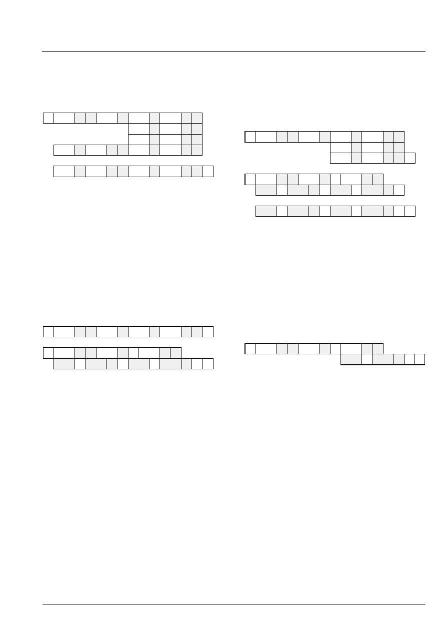
8,o2
o1,o0
S
DW
data_read
W
A
A
S
A
DR
P
P
W
A
d3,d2
A
d1,d0
N
W
d3,d2
A
d1,d0
....repeat for n data values....
W
S
DW
data_write
W
A
A
A
W
A
9,r1
r0,d4
A
W
A
P
d3,d2
d1,d0
PRELIMINARY DATA SHEET
MAS 3506D
Micronas
19
3.3.7. Write Memory (Codes A
hex
and B
hex
)
The memory areas D0 and D1 can be written by using
the codes a
hex
and b
hex
, respectively.
With the Write D0/D1 Memory command n 20-bit
memory cells in D0 can be initialized with new data.
Example: Write 80234
hex
to D1:456 has the following
I
2
C protocol:
<3a 68 b0 00
write D1 memory
00 01
1 word to write
04 56
start address
00 08
value = 80234
hex
02 34>
3.3.8. Read Register (Code D
hex
)
The MAS 3506D has an address space of 256 DSP-
registers. Some of the registers (r = r1,r0 in the figure
above) are direct control inputs for various hardware
blocks, others control the internal program flow. In
Table 3≠10, the registers of interest are described in
detail. In contrast to memory cells, registers cannot be
accessed as a block but must always be addressed
individually.
Example:
Read the content of the register c8
hex
:
<3a 68 dc 80>
define register
<3a 69 <3b
xx xd dd dd
>
and read
3.3.9. Read Memory (Codes E
hex
and F
hex
)
The MAS 3506D has 2 memory areas called D0 and
D1 using the codes e
hex
and f
hex
for their read com-
mands, respectively.
The Read D0/D1 Memory command gives the control-
ler access to all 20 bits of the memory cells of the
MAS 3506D. The telegram for reading 3 words starting
at location D1:100 is
<3a 68 f0 00 00 03 01 00>
<3a 69 <3b
xx xd dd dd
xx xd dd dd
xx xd dd dd
>
3.3.10.Default Read
The Default Read command immediately returns the
lower 16 bits of the main status cell ("Status") of the
MAS 3506D and may be used to poll the processor
status. The meaning of the returned bits is given in the
description of control memory cell D1:7ee in Table 3≠
11 on page 23.
S
DW
data_write
W
A
A
A
W
A
a,0
0,0
W
A
x,x
A
x,d4
P
A
W
A
n3,n2
n1,n0
A
W
A
a3,a2
a1,a0
W
A
d3,d2
A
d1,d0
W
A
x,x
A
x,d4
W
A
d3,d2
A
d1,d0
....repeat for n data values....
1) send command
2) get register value
S
DW
data_write
W
A
A
A
W
A
P
d,r1
r0,0
S
DW
data_read
W
A
A
W
N
d3,d2
S
A
DR
A
d1,d0
P
W
A
x,x
A
x,d4
W
1) send command (Read D0)
2) get register value
S
DW
data_write
W
A
A
A
W
A
e,0
0,0
S
DW
data_read
W
A
A
W
A
x,x
S
A
DR
A
x,d4
P
A
W
A
n3,n2
n1,n0
A
W
A
P
a3,a2
a1,a0
W
A
d3,d2
A
d1,d0
W
A
N
x,x
A
x,d4
W
d3,d2
A
d1,d0
....repeat for n data values....
W
W
S
DW
data_read
W
A
A
N
S
A
DR
P
W
d3,d2
A
d1,d0
W
MAS 3506D
PRELIMINARY DATA SHEET
20
Micronas
3.4. Control Registers
The registers displayed in the following table can be
read and written via I
2
C commands described (see
Section 3.3.6. and Section 3.3.8.).
Note! Registers not given in the tables must not be
written.
Table 3≠10: Control Registers
Address
(hex)
R/W
Function
Default
(hex)
Name
8e
W
DC/DC-Converter Frequency and Voltage
The I
2
C protocol is working only if the processor is active
(WSEN = 1). However, the setting for the DCCF register will
remain active if the WSEN line is deasserted.
08000
DCCF
DC/DC-Converter Frequency
The frequency is controlled with bits 13...10 and 8.
Setting
bit [13:10]
Frequency/kHz
bit [8] = 0
Frequency/kHz
bit [8] = 1
11 11
11 10
11 01
11 00
10 11
10 10
10 01
10 00
01 11
01 10
01 01
01 00
00 11
00 10
00 01
00 00
156
160
163
167
171
175
179
184
188
194
199
204
210
216
223
230
128
245
253
263
272
283
295
307
320
335
351
368
387
409
433
460
The divider for the CLKI input is determined by the content of the
DCCF register. This register allows 32 settings of the DC/DC con-
verter clock frequency f
dc
:
(EQ 1)
In order to reduce interference noise in AM-reception, the oscillator
frequency may be adjusted in 16 steps in order to allow the system
controller to select a base frequency that does not interfere with an
other application. The following algorithm may be used to select an
appropriate value for DCCF:
f
SW
f
CK LI
2
m
n
+
(
)
-------------------------
=
n
0 15
{ ,
}
m
16 32
,
{
}
,
PRELIMINARY DATA SHEET
MAS 3506D
Micronas
21
8e
continued
int selectfrequency(double fstation) {
double fq,fdiv;
double fqmax = 0;
int imax = 0;
for (int i=0;i<16;i++) {
fdiv = 14725000/(2*(32+i));
fq = fstation/fdiv;
fq = fabs(fq-floor(fq)-0.5)*fdiv;
if (fq > fqmax) imax = i;
}
return imax;
}
Modifications to this algorithm are applicable. It may be useful to
finish this procedure if fqmax reaches a certain minimum value, or
a preprocessed table for all possible AM-carrier frequencies may
be stored in ROM for the controller.
DCCF
continued
DC/DC-Converter Voltage
The output voltage is selected with bits 16...14 and 9. There is a
threshold between the output voltage of the DC/DC converter and
the internal voltage monitor. The PUP signal becomes inactive
when the output drops below the monitor voltage.
Setting
bit [16:14] and [9]
DC/DC-Converter
Output Voltage/V
Internal Monitor
Voltage/V
1 11
0
1 10 0
1 01 0
1 00 0
0 11
0
0 10 0
0 01 0
0 00 0
1 11
1
1 10 1
1 01 1
1 00 1
0 11
1
0 10 1
0 01 1
0 00 1
3.57
3.46
3.35
3.25
3.14
3.04
2.94
2.83
2.73
2.63
2.52
2.42
2.32
2.22
2.12
2.02
3.38
3.27
3.16
3.06
2.95
2.85
2.75
2.64
2.54
2.44
2.33
2.23
2.13
2.03
1.93
1.82
Table 3≠10: Control Registers, continued
Address
(hex)
R/W
Function
Default
(hex)
Name

MAS 3506D
PRELIMINARY DATA SHEET
22
Micronas
c8
R
PIO-Register
The PIO-register is used to monitor the actual status of the PIO-
pins for both, PIO-output and PIO-input lines. Bit 0 of the PIO reg-
ister corresponds to pin PI0, bit 1 to PI1 etc. Due to the latency of
the MAS 3506D only slow events (>1 ms) can be monitored.
Please also refer to Section 4.6.3.2.
bit [19]
BC-FRAME-TOGGLE
Output level toggles with each BC-frame,
t
frame
= 432 ms
bit [18]
BCENABLE
0
use SID*, SII*, SIC*
1
use SID, SII, SIC
bit [13]
BC-FRAME-SYNC
0
cleared after SCH-read operation
1
start of new frame
bit [12]
BC-SYNC
0
unsynchronized
1
synchronized to BC
bit [8]
Decoding-ERROR
0
no error
1
error or sync lost
bit [4]
MPEG-FRAME-SYNC
0
cleared after anciliary data were read
1
sync to a new MPEG-frame
bit [3]
AUD-SW
This bit may be used to monitor a signal
from the headphone jack that indicates
switching between headphone and
loudspeaker mode.
bit [2:0]
These three free input lines return the
state logic level of the respective PIO-
pins. They may be used as a port
expansion of the controller.
PIO
Table 3≠10: Control Registers, continued
Address
(hex)
R/W
Function
Default
(hex)
Name

PRELIMINARY DATA SHEET
MAS 3506D
Micronas
23
3.5. Control and Status Memory
The memory cells given in the following sections may
be read (Section 3.3.9.) or written (Section 3.3.7.) in
order to observe or control the operation of the
MAS 3506D.
Note! Memory cells not given in the tables must not be
written.
Table 3≠11: Control and status memory cells
Address
(hex)
R/W
Function
Default
Name
D1:7ee
R
Main Status Indicator of the BC-Decoder
The Status cell returns global status information about the World-
Space decoder. Its value is also returned by the `Default Read'
command as described in Section 3.3.10.
bit [15:12] BRI
Bit Rate Index
0
Reserved
1...8
n*16 kbit/s
bit [11:8]
NSC
Zero-based number of available Service
Components
0
1 SC available
...
...
7
8 SCs available
bit [7:4]
reserved
bit [3]
MCRC
MPEG CRC Error
0
no CRC-error in the last BC-frame
1
CRC-error occured in the last BC-frame
bit [2]
MFS
MPEG frame sync indication
0
no MPEG synchronisation
1
MPEG synchronisation
bit [1]
BCS
Broadcast Channel frame sync indication
0
no BC synchronisation
1
BC synchronisation
While the signals MPEG-FRAME-SYNC and BC-FRAME-SYNC in
the PIO-register c8
hex
rise with the beginning of each frame, the
signals MFS and BFS are stable as long as a valid bitstream is
received.
bit [0]
S
Synchronized state
0
not in synchronized state (e.g. no bitstream)
1
MAS 3506D is synchronized and decoding
Status

MAS 3506D
PRELIMINARY DATA SHEET
24
Micronas
D1:7ef
R/W
Service Component Selection (0..7) and Decoding Control
bit [15]
OutputMute
0
normal operation
1
mute output
bit [14]
AutoScan Autoscan function
0
disable autoscan function
1
enable autoscan function,
skip non-audio SCs
bit [13]
BCChange Broadcast Channel Change
0
cleared on SCH-rescynchronization
1
clears all previous SCH-information
Setting this bit clears all previous SCH-information and thus pre-
pares the MAS 3506D for a BC-change. This ensured the availabil-
ity of the correct SCH-data for the new BC.
bit [12]
MPEGResync
0
allows resynchronization only after
SCH-detection
1
MPEG-resynchronization enabled
bit [11:3]
reserved, set to 0
bit [2:0]
SC
Zero-based number of audio Service
Component to be decoded
0
decode SC 1
...
7
decode SC 8
NumSC
D1:7f0
R/W
Counter for Broadcast Channel Frames
bit [15:0]
BCCount
Counter for the decoded Broadcast
Channel frames
The BCFrameCnt ist incremented by one for each successfully
decoded BC-frame (432 ms) since reset. This address is writable,
thus the controller may reset/preset the content at any time to an
arbitrary value.
BCFrameCnt
D1:7f1
R/W
Counter for MPEG Frames
bit [15:0]
MPEGFrameCnt
Counter for the decoded MPEG-frames
The MPEGFrameCnt ist incremented by one for each successfully
decoded MPEG-frame (24...72 ms) since reset. This address is
writable for a reset/preset.
MPEG-
FrameCnt
Table 3≠11: Control and status memory cells, continued
Address
(hex)
R/W
Function
Default
Name
PRELIMINARY DATA SHEET
MAS 3506D
Micronas
25
D1:7f3
R
System Error Indication
bit [10:0]
ErrorCode Last error of WorldSpace decoding
1xx
hex
Buffer problem, causes a firmware reset:
100
hex
ErrorInputTimeOut: Input time-out
101
hex
ErrorServicePreambleWrong: Service
preamble wrong
102
hex
ErrorBufferOverflow: Input buffer overflow
103
hex
ErrorBufferUnderrun: Buffer underflow
104
hex
ErrorOutputTimeout: Output time-out
105
hex
ErrorBitrateIntexChanged: Bitrate index
has changed
106
hex
ErrorNoLayer3SyncNextFram: No synchro-
nization found in input bitstream
2xx
hex
BC-error, causes a BC-resynchronization:
100
hex
ErrorSCToDecodeOutOfRange: SC to
decode is not available
101
hex
ErrorSCTypeWrong: SC has no audio
1ff
hex
ErrorStartBCSync: The controller has
indicated a BC-change (signal BCChange)
3xx
hex
MPEG-error, causes an MPEG-
resynchronization:
300
hex
ErrorSCToDecodeUserChange: A new SC
was selected
301
hex
Error:
302
hex
Error:
303
hex
Error: Sampling rate changed
If an error occurs during decoding of the Broadcast Channel bit-
stream a number describing the error will be copied into this mem-
ory cell. The content always keeps a value corresponding to the
last detected error.
ErrorCode
D1:7f4
R/W
Counter for All Decoding Errors
bit [15:0]
ErrorCnt
Counter for all decoding errors
The ErrorCnt is incremented by one for each decoding error since
reset. This address is writable for a reset/preset. This counter is
valuable for long-time observations. For identification of the last
error see D1:7f3
ErrorCnt
Table 3≠11: Control and status memory cells, continued
Address
(hex)
R/W
Function
Default
Name

MAS 3506D
PRELIMINARY DATA SHEET
26
Micronas
D1:7f5
R
Bits 12..16 of MPEG-Header
The MPEGStatus1 memory cell provides a direct copy of bits
16...12 of the acual MPEG-header. This cell will be updated imme-
diatley after the MPEG-header has beed read from the bitstream.
bit [12:8]
Copy of bits 16...12 of the MPEG-header
bit [12:11] MPEGID
Bits 13 and 12 of the MPEG-header
00
MPEG 2.5
01
reserved
10
MPEG 2
11
MPEG 1
bit [10:9]
Layer
Bits 11 and 10 of the MPEG-header
00
reserved
01
Layer 1*
10
Layer 2*
11
Layer 3
bit [8]
Protection
0
CRC-protected
1
no CRC
bit [7]
reserved
bit [6:2]
private bits
bit [1]
CRC Error
0
no error
1
a CRC-error has occured
bit [0]
Invalid Frame
0
normal operation
1
an invalid frame has occured
MPEGStatus1
Table 3≠11: Control and status memory cells, continued
Address
(hex)
R/W
Function
Default
Name
PRELIMINARY DATA SHEET
MAS 3506D
Micronas
27
D1:7f6
R
Bit 32...17 of MPEG-Header
The MPEGStatus2 memory cell provides a direct copy of bits
32...17 of the acual MPEG-header. This cell will be updated imme-
diately after the MPEG-header has beed read from the bitstream.
MPEGStatus2
MPEG 1
Layer 3
MPEG 2
Layer 3
MPEG 2.5
Layer 3
bit[15:12]
Datarate in kbit/s
0000
0001
0010
0011
0100
0101
0110
0111
1000
1001
1010
1011
1100
1101
1110
1111
free
32
40
48
56
64
80
96
112
128
160*
192*
224*
256*
320*
reserved
free
8
16
24
32
40
48
56
64
80
96
112
128
144*
160*
reserved
free
8
16
24
32
40
48
56
64
80
96
112
128
144*
160*
reserved
bit[11:10]
Sampling frequency/kHz
00
01
10
11
44.1*
48
32
reserved
22.05*
24
16
reserved
11.025*
12
8
reserved
bit[9]
padding bit
bit[8]
private bit
bit[7:6]
Mode
00
stereo
01
joint stereo
10
dual channel
11
reserved
bit[5:4]
Joint stereo: Mode extension
intensity stereo
ms_stereo
00
off
off
01
on
off
10
off
on
11
on
on
bit[3]
Copyright
0
not protected
1
protected
bit[2]
Original/Copy
0
copy
1
original
Table 3≠11: Control and status memory cells, continued
Address
(hex)
R/W
Function
Default
Name
MAS 3506D
PRELIMINARY DATA SHEET
28
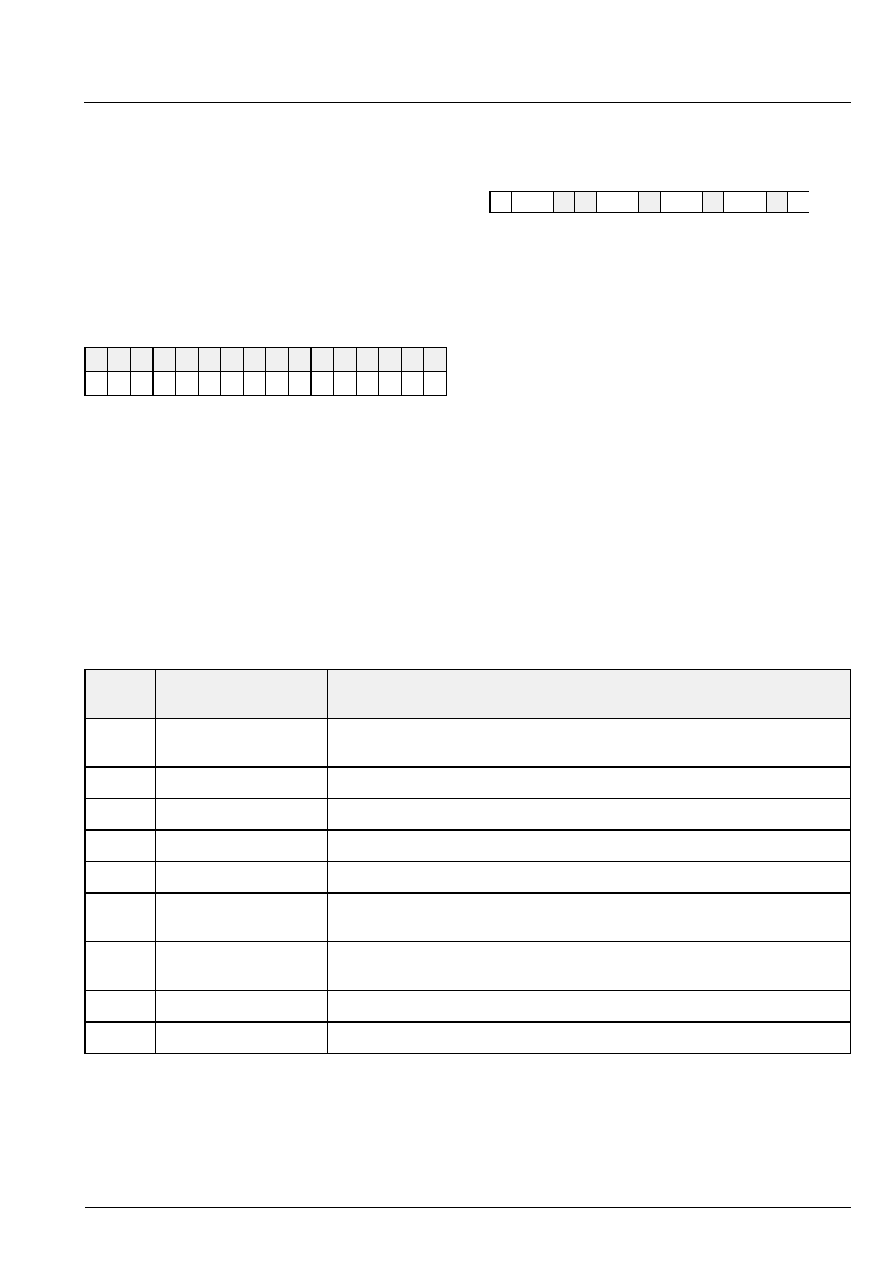
Micronas
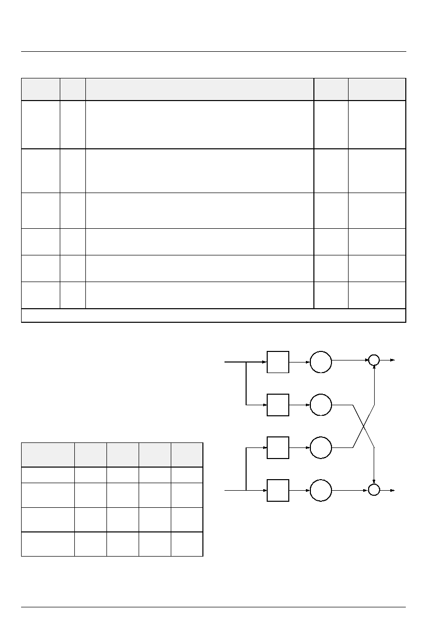
3.5.1. Volume Matrix
The digital baseband volume matrix is used for control-
ling the digital gain as shown in Fig. 3≠2. Table 3≠12
shows the proposed settings for the four volume matrix
coefficients for stereo, left, and right mono. The gain
factors are given in fixed point notation as desribed in
Section 3.3.1.
Fig. 3≠2: Digital volume matrix
D1:7f6
continued
bit[1:0]
Emphasis
00
none
01
50/15 µs
10
reserved
11
CCITT J.17
D1:7f7
R/W
Configures the Serial Audio Output Interface
bit [19:0]
OutputConfig
0
generate 32-bit audio samples
16
generate 16-bit audio samples
OutputConfig
D1:7f8
R/W
Left
Left Gain
bit [19:0]
LL
left
left gain (please refer to Sections
3.3.1. and 3.5.1.)
80000
LL
D1:7f9
R/W
Left
Right Gain
bit [19:0]
LR
left
right gain
00000
LR
D1:7fa
R/W
Right
Left Gain
bit [19:0]
RL
right
left gain
00000
RL
D1:7fb
R/W
Right
Right Gain
bit [19:0]
RR
right
right gain
80000
RR
* Modes marked with an asterisk are not used in the WorldSpace system.
Table 3≠11: Control and status memory cells, continued
Address
(hex)
R/W
Function
Default
Name
Table 3≠12: Settings for the digital volume matrix
Memory lo-
cation (hex)
D1:
7f8
D1:
7f9
D1:
7fa
D1:
7fb
Name
LL
LR
RL
RR
Stereo
(default)
-
1.0
0
0
-
1.0
Mono
left
-
1.0
-
1.0
0
0
Mono
right
0
0
-
1.0
-
1.0
-
1
-
1
-
1
-
1
LL
LR
RL
RR
+
+
left audio
right audio
PRELIMINARY DATA SHEET
MAS 3506D
Micronas
29
Table 3≠13: Volume matrix conversion (dB into hexadecimal)
Volume
(in dB)
Hexa
decimal
Volume
(in dB)
Hexa
decimal
Volume
(in dB)
Hexa
decimal
Volume
(in dB)
Hexa
decimal
Volume
(in dB)
Hexa
decimal
0
80000
-
20
F3333
-
40
FEB85
-
60
FFDF4
-
80
FFFCC
-
1
8DEB8
-
21
F4979
-
41
FEDBF
-
61
FFE2D
-
81
FFFD1
-
2
9A537
-
22
F5D52
-
42
FEFBB
-
62
FFE60
-
82
FFFD6
-
3
A5621
-
23
F6F03
-
43
FF180
-
63
FFE8D
-
83
FFFDB
-
4
AF3CD
-
24
F7EC8
-
44
FF314
-
64
FFEB5
-
84
FFFDF
-
5
B8053
-
25
F8CD5
-
45
FF47C
-
65
FFED9
-
85
FFFE3
-
6
BFD92
-
26
F995B
-
46
FF5BC
-
66
FFEF9
-
86
FFFE6
-
7
C6D31
-
27
FA485
-
47
FF6DA
-
67
FFF16
-
87
FFFE9
-
8
CD0AD
-
28
FAE78
-
48
FF7D9
-
68
FFF2F
-
88
FFFEB
-
9
D2958
-
29
FB756
-
49
FF8BC
-
69
FFF46
-
89
FFFED
-
10
D785E
-
30
FBF3D
-
50
FF986
-
70
FFF5A
-
90
FFFEF
-
11
DBECC
-
31
FC648
-
51
FFA3A
-
71
FFF6C
-
91
FFFF1
-
12
DFD91
-
32
FCC8E
-
52
FFADB
-
72
FFF7C
-
92
FFFF3
-
13
E3583
-
33
FD227
-
53
FFB6A
-
73
FFF8B
-
93
FFFF4
-
14
E675F
-
34
FD723
-
54
FFBEA
-
74
FFF97
-
94
FFFF6
-
15
E93CF
-
35
FDB95
-
55
FFC5C
-
75
FFFA3
-
95
FFFF7
-
16
EBB6A
-
36
FDF8B
-
56
FFCC1
-
76
FFFAD
-
96
FFFF8
-
17
EDEB6
-
37
FE312
-
57
FFD1B
-
77
FFFB6
-
97
FFFF9
-
18
EFE2C
-
38
FE638
-
58
FFD6C
-
78
FFFBE
-
98
FFFF9
-
19
F1A36
-
39
FE905
-
59
FFDB4
-
79
FFFC5
-
99
FFFFA
MAS 3506D
PRELIMINARY DATA SHEET
30
Micronas
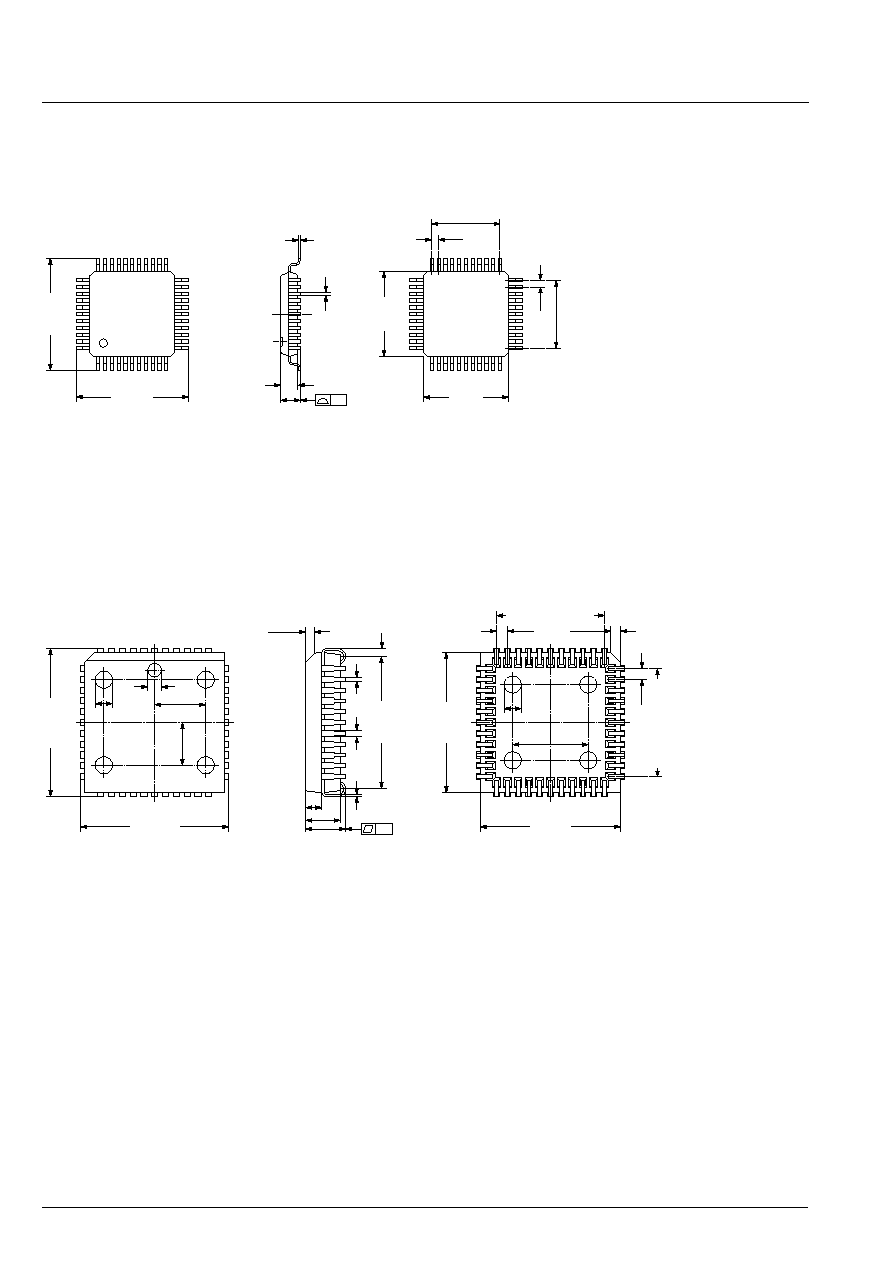
4. Specifications
4.1. Outline Dimensions
Fig. 4≠1:
44-Pin Plastic Metric Quad Flat Package
(PMQFP44)
Weight approximately 0.4g
Dimensions in mm
Fig. 4≠2:
44-Pin Plastic Leaded Chip Carrier Package
(PLCC44)
Weight approximately 2.5 g
Dimensions in mm
Note: The PLCC44-package has limited availability
Caution: Start pin and orientation of pin numbering is different for PLCC and PMQFP-housings.
SPGS706000-5(P44)/1E
34
44
1
11
12
22
23
33
0.1
0.8
0.8
13.2
0.2
±
13.2
0.2
±
0.17
0.06
±
2.15
0.2
±
2.0
0.1
±
0.34
0.05
±
10
0.1
±
10
0.1
±
10 x 0.8 = 8
0.1
±
10 x 0.8 = 8
0.1
±
15.7
0.3
±
10 x 1.27 = 12.7
0.1
±
1.2 x 45
∞
1
40
39
29
28
18
17
7
6
1.6
0.1
6
8.6
6
2
2
x 45
∞
1.1
1.27
1.27
SPGS704000-1(P44/K)/1E
17.52
0.12
±
17.52
0.12
±
16.5
0.1
±
16.5
0.1
±
10 x 1.27 = 12.7
0.1
±
4.75
±
0.15
4.05
±
0.1
1.9
±
0.05
0.27
0.03
±
0.71
0.05
±
0.48
0.06
±
0.9
0.2
±
PRELIMINARY DATA SHEET
MAS 3506D
Micronas
31
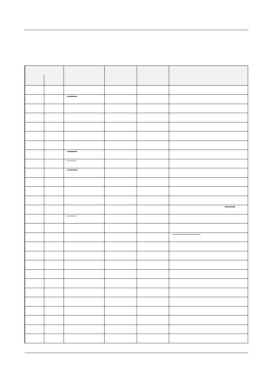
4.2. Pin Connections and Short Descriptions
NC
not connected, leave vacant
X
obligatory, pin must be connected as
described in application informations
LV
if not used, leave vacant
VDD
connect to positive supply
VSS
connect to ground
Pin No.
Pin Name
Type
Connection
Short Description
PMQFP
44-pin
PLCC
44-pin
(If not used)
1
6
TE
I
VSS
Test enable
2
5
POR
I
VDD
Reset , active low
3
4
I2CC
IO
X
I
2
C clock line
4
3
I2CD
IO
X
I
2
C data line
5
2
VDD
Supply
X
Positive supply for digital parts
6
1
VSS
Supply
X
Gound supply for digital parts
7
44
DCEN
I
VSS
Start and enable DC/DC converter
8
43
EOD
O
LV
PIO end of DMA, active low
9
42
RTR
O
LV
PIO ready to read, active low
10
41
RTW
O
LV
PIO ready to write, active low
11
40
DCSG
Supply
VSS
DC converter transistor ground
12
39
DCSO
O
VSS
DC converter transistor open drain
13
38
VSENS
I
VDD
DC converter voltage sense
14
37
PR
I
VDD
PIO DMA request or Read/Write
15
36
PCS
I
VDD
PIO chip select , active low
16
35
PI19
O
LV
BC-Frame-Toggle
17
34
PI18
I
VSS
BCINENABLE
18
33
PI17
I
VSS
PIO data [17], reserved
19
32
SIC*/PI16
I
X
PIO data[16] (SIC*)
20
31
SII*/PI15
I
VSS
PIO data[15] (SII*)
21
30
SID*/PI14
I
X
PIO data [14] (SID*)
22
29
PI13
O
LV
BC-FRAME-SYNC
23
28
PI12
O
LV
BC-SYNC
24
27
SOD/PI11
O
LV
Serial output data
25
26
SOI/PI10
O
LV
Serial ouput frame identification
26
25
SOC/PI9
O
LV
Serial output clock
27
24
PI8
O
LV
Decoding-error
28
23
XVDD
Supply
X
Positive supply of output buffers
MAS 3506D
PRELIMINARY DATA SHEET
32
Micronas
29
22
XVSS
Supply
X
Ground of output buffers
30
21
SID/PI7
I
X
Serial input data
31
20
SII/PI6
I
VSS
Serial input frame identification
32
19
SIC/PI5
I
X
Serial input clock
33
18
PI4
O
LV
MPEG-frame sync
34
17
PI3
I
VSS
AUD-SW, information from head-
phone jack
35
16
PI2
I
VSS
Reserved
36
15
PI1
I
VSS
Reserved
37
14
PI0
I
VSS
Reserved
38
13
CLKO
O
LV
Clock output (nominal 24.576 MHz)
39
12
PUP
O
LV
Power Up, i.e. status of voltage super-
vision
40
11
WSEN
I
X
Enable DSP and DC/DC converter
41
10
WRDY
O
LV
If WSEN=0: Valid clock input at CLKI
If WSEN=1: Clock synthesizer PLL
locked
42
9
AVDD
Supply
VDD
Supply for analog circuits
43
8
CLKI
I
X
Clock input
44
7
AVSS
Supply
VSS
Ground supply for analog circuits
Pin No.
Pin Name
Type
Connection
Short Description
PMQFP
44-pin
PLCC
44-pin
(If not used)

PRELIMINARY DATA SHEET
MAS 3506D
Micronas
33
4.3. Pin Descriptions
4.3.1. Power Supply Pins
Connection of all power supply pins is mandatory for
the function of the MAS 3506D.
VDD
SUPPLY
VSS
SUPPLY
The VDD/VSS pair is internally connected with all digi-
tal modules of the MAS 3506D.
XVDD
SUPPLY
XVSS
SUPPLY
The XVDD/XVSS pins are the supply lines for the pin
output buffers.
AVDD
SUPPLY
AVSS
SUPPLY
The AVDD/AVSS pair is internally connected with the
analog blocks of the MAS 3506D, i.e. clock synthe-
sizer and supply voltage supervision circuits.
4.3.2. DC/DC Converter Pins
DCEN
DC/DC ENABLE
IN
The DCEN input signal starts and enables the DC/DC
converter operation.
DCSG
SUPPLY
The DC converter Signal Ground pin is used as a
basepoint for the internal switching transistor of the
DC/DC converter. It must always be connected to
ground.
DCSO
OUT
DCSO is an open drain output and should be con-
nected with external circuitry (inductor/diode) to start
the DC/DC converter. When the DC/DC converter is
not used, it has to be connected to VSS.
VSENS
IN
The VSENS pin is the input for the DC/DC converter
feedback loop. It must be connected directly with the
Schottky diode and the capacitor as shown in Fig. 2≠5
on page 10.
When the DC/DC converter is not used, it has to be
connected to VDD.
4.3.3. Control Lines
I2CC
SCL
IN/OUT
I2CD
SDA
IN/OUT
Standard I
2
C control lines. Normally there are pull-up
resistors from each line to VDD.
4.3.4. Parallel Interface Control Lines
PR
IN
PCS
IN
RTR
OUT
RTW
OUT
EOD
OUT
PIO handshake lines. Their use depends on the actual
firmware on the MAS 3506D. Usage of these lines in
the standard WorldSpace configuration is not planned.
4.3.5. Parallel Interface Data Lines
General purpose Parallel IO pins. The information of
the input and output signals may also be read from
Register c8
hex
(please refer to Table 3≠10 in Section
Section 3.4. on page 20).
PI19
BC-FRAME-TOGGLE
OUT
The BC-FRAME-TOGGLE output toggles its state after
each correctly decoded Broadcast Channel Frame
(432 ms). This pin can be used for monitor the proper
function of the system.
PI18
BCINENABLE
IN
PI18 is used as input pin to sense the status of the
BCINENABLE line at the WorldSpace connector. On
low input level the alternative BC-input lines SIC*, SII*
and SID* are activated and SIC, SII, SID are deacti-
vated.
PI17
RESERVED
IN/OUT
PI16
SIC*
IN
PI15
SII*
IN
PI14
SID*
IN
The SIC*, SID*, and SII* may be configured as alterna-
tive serial input lines in order to support alternative
serial digital sources. SID* (PI14) is used as Broadcast
Channel data input from the Broadcast Channel I/O
interface.

MAS 3506D
PRELIMINARY DATA SHEET
34
Micronas
PI13
BC-FRAME-SYNC
OUT
The BC-FRAME-SYNC is reset after POR and set to
`1' after each correctly decoded SCH. It will only be
cleared if the controller reads out SCH information
from the MAS 3506D.
PI12
BC-SYNC
OUT
The BC-SYNC is set, if the MAS 3506D is in the state
of proper decoding of the Broadcast Channel bit-
stream.
PI8
DECODING-ERROR
OUT
The Decoding-Error pin is activated, if during decoding
of the Broadcast Channel, the MPEG frame an error
occurs or if no input bitstream is applied.
PI4
MPEG-FRAME-SYNC
IN
The MPEG-FRAME-SYNC signal indicates that an
MPEG header has been decoded properly and the
internal MPEG decoder is in a synchronized state. The
MPEG-FRAME-SYNC signal is inactive after Power-
On Reset and will be activated when a valid MPEG
Layer 3 header has been recognized. The signal will
be cleared if the ancillary data information is read out
by the controller via I
2
C interface.
PI3
AUD-SW
IN
The AUD-SW input may sense the headphone jack
and deposit its information in Bit 3 of register c8
hex
(please refer to Table 3≠10 on page 20.) This way the
controller can get the information weather a loud-
speaker or a headphone should be supplied and can
set the BAS_INVR bit in DRD 3515A's register
GLB_CONFIG accordingly.
PI2
RESERVED
IN
PI1
RESERVED
IN
PI0
RESERVED
IN
4.3.6. Voltage Supervision And Other Functions
CLKI
IN
CLKO
OUT
CLKI and CLKO are the input and output clock lines to
be connected to the DRD 3515A. CLKI expects
14.725 MHz, CLKO delivers 24.576 MHz synchronous
to the audio data stream.
PUP
POWER UP
OUT
The PUP output indicates that the power supply volt-
age exceeds its minimal level (software adjustable).
WSEN
DSP ENABLE
IN
WSEN enables DSP and DC/DC-converter operation.
It must also be set to activate the control interface e.g.
to reprogram the DC/DC-converter.
WRDY
OUT
WRDY has two functionalities depending on the state
of the WSEN signal.
If WSEN = 0, it indicates that a valid clock has been
recognized at the CLKI clock input.
If WSEN = 1, the WRDY output will be set to `0' until
the internal clock synthesizer has locked to the incom-
ing audio data stream, and thus, the CLKO clock out-
put signal is valid.
4.3.7. Serial Input Interface
SID
IN
SII
IN
SIC
IN
Data, Frame Indication and Clock line of the serial
input interface. The SII line should be connected with
VSS in the standard WorldSpace mode. The SID and
SIC lines are used for the Broadcast Channel input.
PRELIMINARY DATA SHEET
MAS 3506D
Micronas
35
4.3.8. Serial Output Interface
SOD
OUT
SOI
OUT
SOC
OUT
Data, Frame Indication and Clock line of the serial
audio output interface (I
2
S). The SOC line can be
deactivated, if only the DRD 3515A D/A converter is
connected. The SOI indicates, whether the left or the
right audio sample is transmitted. In the default setting
a left audio sample always corresponds to SOI = low.
4.3.9. Miscellaneous
POR
IN
The Power-On Reset pin is used to reset the digital
parts of the MAS 3506D.
TE
IN
The TE pin is for production test only and must be con-
nected with VSS in all applications.
4.4. Pin Configuration
Fig. 4≠3: PMQFP44 package
Fig. 4≠4: PLCC44 package
34
35
36
37
38
39
40
41
42
43
44
22
21
20
19
18
17
16
15
14
13
12
1
2
3
4
5
6
7
8
9
10 11
33 32 31 30 29 28 27 26 25 24 23
PI3
PI2
PI1
PI0
CLKO
PUP
WSEN
WRDY
AVDD
CLKI
AVSS
PI13
SID
SII
SIC
PI17
PI18
PI19
PCS
PR
VSENS
DCSO
SIC
SII
SID
XVSS
XVDD
PI4
PI8
SOC
SOI
SOD
PI12
POR
I2CC
I2CD
VDD
VSS
TE
DCEN
EOD
RTR
RTW
DCSG
MAS 3506D
7
8
9
10
11
12
13
14
15
16
17
39
38
37
36
35
34
33
32
31
30
29
18 19 20 21 22 23 24 25 26 27 28
6
5
4
3
2
1
44 43 42 41 40
AVSS
CLKI
AVDD
WRDY
WSEN
PUP
CLKO
PI0
PI1
PI2
PI3
DCSO
VSENS
PR
PCS
PI19
PI18
PI17
SIC
SII
SID
PI13
POR
I2CC
I2CD
VDD
VSS
TE
DCEN
EOD
RTR
RTW
DCSG
SIC
SII
SID
XVSS
XVDD
PI4
PI8
SOC
SOI
SOD
PI12
MAS 3506D
MAS 3506D
PRELIMINARY DATA SHEET
36
Micronas
4.5. Internal Pin Circuits
Fig. 4≠5: Input pins PCS, PR
Fig. 4≠6: Input pin TE, DCEN
Fig. 4≠7: Input pins WSEN, POR
Fig. 4≠8: Input pin CLKI
Fig. 4≠9: Input/Output pins PI0...PI4, PI8, SOC, SOI,
SOD, PI12...PI19
Fig. 4≠10: Input/Output pins I2CC, I2CD
Fig. 4≠11: Input/Output pins DCSO, DCSG
Fig. 4≠12: Output pins WRDY, RTW, EOD, RTR,
CLKO, PUP
Fig. 4≠13: Input pin VSENS
Fig. 4≠14: Input/Output pins SIC, SII, SID
TTLIN
XVDD
P
N
XVSS
VDD
N
VSS
DCSO
DCSG
VSS
XVDD
XVSS
N
P
VSENS
VSS
XVDD
P
N
XVSS
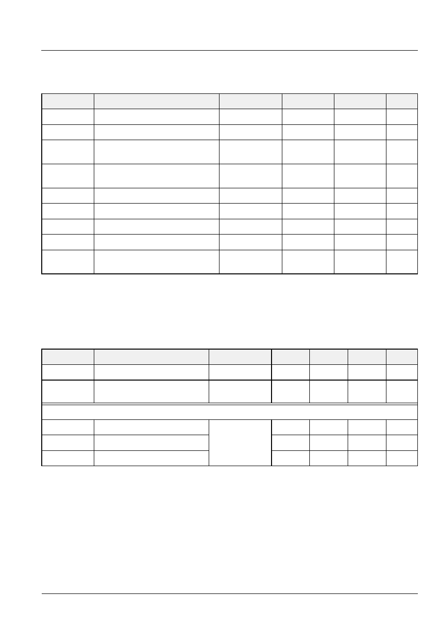
PRELIMINARY DATA SHEET
MAS 3506D
Micronas
37
4.6. Electrical Characteristics
4.6.1. Absolute Maximum Ratings
Stresses beyond those listed in the "Absolute Maximum Ratings" may cause permanent damage to the device. This
is a stress rating only. Functional operation of the device at these or any other conditions beyond those indicated in
the "Recommended Operating Conditions/Characteristics" of this specification is not implied. Exposure to absolute
maximum ratings conditions for extended periods may affect device reliability.
4.6.2. Recommended Operating Conditions
Symbol
Parameter
Pin Name
Min.
Max.
Unit
T
A
Ambient operating temperature
-
40
85
∞C
T
S
Storage temperature
-
40
125
∞C
P
MAX
Power dissipation
VDD, XVDD,
AVDD
600
mW
V
SUP
Supply voltage
VDD, XVDD,
AVDD
5.5
V
V
Idig
Input voltage, all digital inputs
-
0.3
V
SUP
+0.3
V
I
Idig
Input current, all digital inputs
-
20
+20
mA
I
Out
Current, all digital output
0.5
A
I
OutDC
Current
DCSO
1.5
A
V
II2C
Input voltage, I
2
C-Pins
I2CC,
I2CC
-
0.3
5.5
V
Symbol
Parameter
Pin Name
Min.
Typ.
Max.
Unit
T
A
Ambient temperature range
-
40
85
∞C
V
SUP
Supply voltage
VDD, XVDD,
AVDD
2.7
3.0
3.6
V
Reference Frequency Generation
CLK
F
Clock frequency
CLKI
14.725
MHz
CLK
I_V
Clock input voltage
0
V
SUP
V
CLK
Amp
Clock amplitude
0.5
V
pp
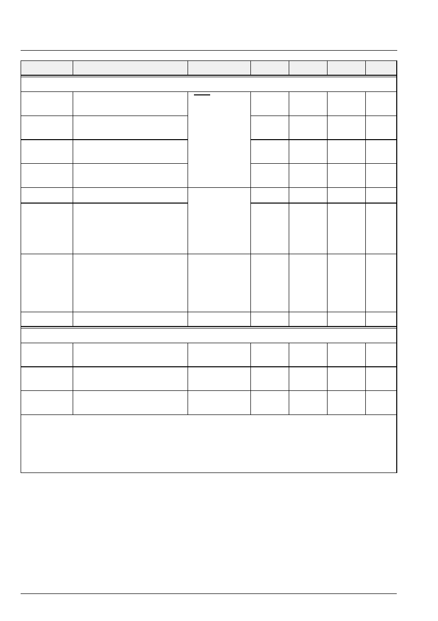
MAS 3506D
PRELIMINARY DATA SHEET
38
Micronas
Levels
I
IL27
Input low voltage
at V
SUP
= 2.7 V ... 3.6 V
POR
I2CC,
I2CD,
DCEN,
WSEN
0.4
V
I
IH36
Input high voltage
at V
SUP
= 2.7 V ... 3.6 V
1.8
V
I
IH33
Input high voltage
at V
SUP
= 2.7 V ... 3.3 V
1.7
V
I
IH30
Input high voltage
at V
SUP
= 2.7 V ... 3.0 V
1.6
V
I
ILD
Input low voltage
PI<i>
1)
,
SII,
SIC,
SID,
PR,
PCS,
TE,
0.4
V
I
IHD
Input high voltage
V
SUP
-
0.5
V
T
rf
Rise/fall time of digital inputs
PI<i>,
SII,
SIC,
SID,
PR,
PCS, CLKI
10
ns
D
cycle
Duty cycle of digital clock inputs
SIC, CLKI
40
50
60
%
DC-DC converter external circuitry
C
1
Blocking capacitor
(< 100 m
ESR)
2)
VSENS, DCSG
330
µ
F
V
F
Schottky diode forward voltage
3)
DCSO,
VSENS
0.35
V
L
Inductance of ferrite ring core
coil
4)
DCSO
22
µ
H
1)
i = 0 to 4, 8 , 12 to 19
2)
Sanyo Oscon 6SA330M
(distributed by Endrich Bauelemente, D-72202 Nagold-lselshausen)
3)
ZETEX ZMCS1000
(distributed by ZETEX, D-81673 M¸nchen), standard Schottky 1N5817
4)
C8 R/4L, SDS0604 (distributed by Endrich Bauelemente, see above)
Symbol
Parameter
Pin Name
Min.
Typ.
Max.
Unit
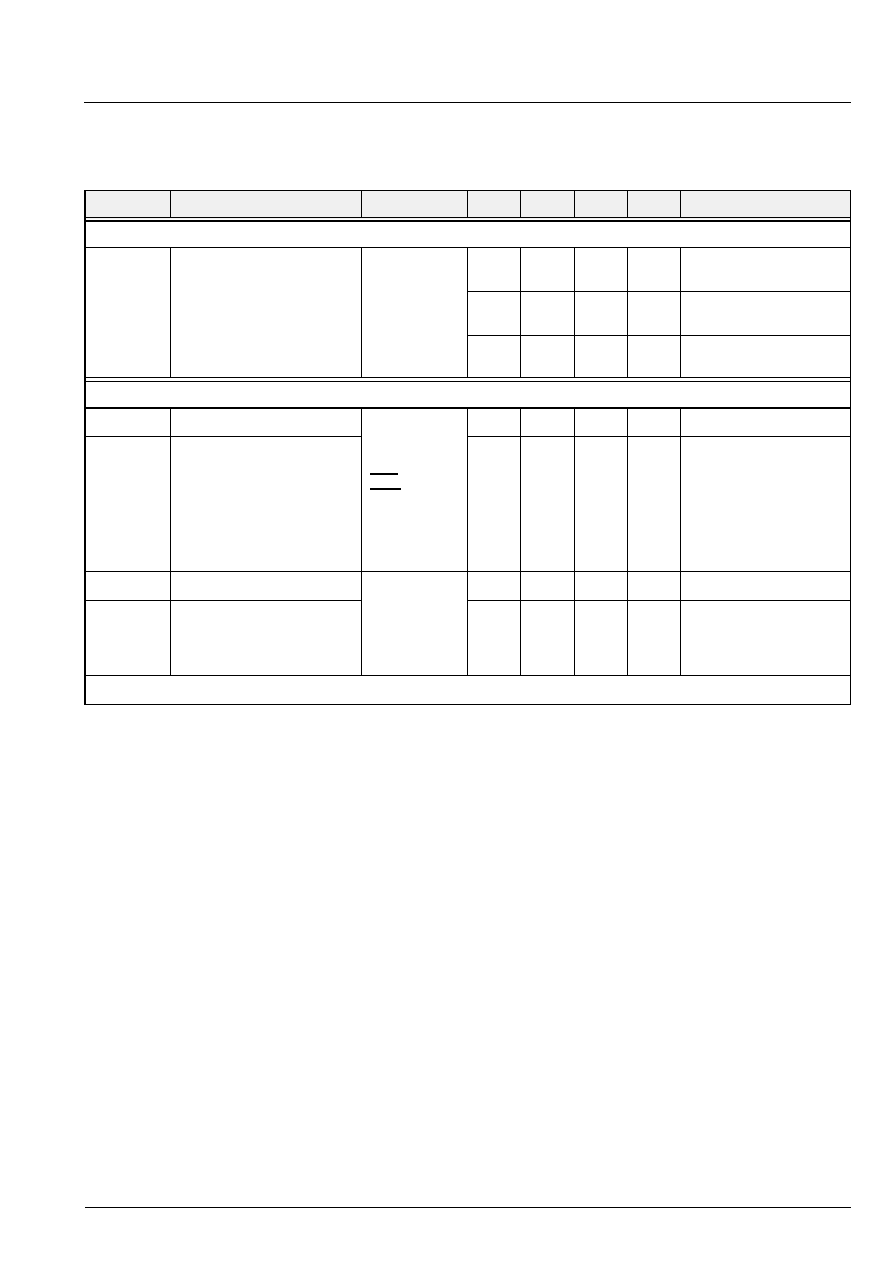
PRELIMINARY DATA SHEET
MAS 3506D
Micronas
39
4.6.3. Characteristics
at T = T
A
, V
SUP
= 2.7 to 3.6 V, typ. values at T
A
= 27∞C, V
SUP
= 3.5 V, CLK
F
= 14.725 MHz, duty cycle = 50%
Symbol
Parameter
Pin Name
Min.
Typ.
Max.
Unit
Test Conditions
Supply Voltage
I
SUP
Current consumption
VDD, XVDD,
AVDD
32
mA
2.7 V, sampling
frequency
32kHz
17
mA
2.7 V, sampling
frequency
24 kHz
11
mA
2.7 V, sampling
frequency
12 kHz
Digital Outputs and Inputs
V
DOL
Output low voltage
SOI
1)
,
SOC
1)
,
SOD
1)
,
EOD,
RTR,
RTW,
WRDY,
PUP,
CLKO
PI<i>
0.3
V
I
load
= 6mA
V
DIH
Output high voltage
V
SUP
-
0.3
V
I
load
= 6mA
Z
DigI
Input impedance
PI<i>,
SII,
SIC,
SID,
PR,
PCS, CLKI
7
pF
I
DLeak
Digital input leakage current
-
1
1
µ
A
0 V < V
pin
< V
SUP
1)
in low impedance mode
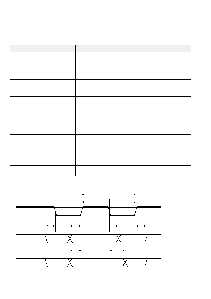
MAS 3506D
PRELIMINARY DATA SHEET
40
Micronas
4.6.3.1. I
2
C Characteristics
at T = T
A
, V
SUP
=2.7 to 3.6 V, typ. values at T
A
= 27∞C, V
SUP
= 3.0 V, CLK
F
= 14.725 MHz, duty cycle = 50 %
Fig. 4≠15: I
2
C timing diagram
Symbol
Parameter
Pin Name
Min.
Typ.
Max.
Unit
Test Conditions
R
ON
Output resistance
I2CC,
I2CD
60
I
load
= 5 mA,
V
SUP
= 2.7 V
f
I2C
I
2
C bus frequency
I2CC
400
kHz
t
I2C1
I
2
C Start condition setup time
I2CC,
I2CD
300
ns
t
I2C2
I
2
C Stop condition setup time
I2CC,
I2CD
300
ns
t
I2C3
I
2
C clock low pulse time
I2CC
1250
ns
t
I2C4
I
2
C clock high pulse time
I2CC
1250
ns
t
I2C5
I
2
C data hold time before
rising edge of clock
I2CC
80
ns
t
I2C6
I
2
C data hold time after falling
edge of clock
I2CC
80
ns
V
I2COL
I
2
C output low voltage
I2CC,
I2CD
0.3
V
I
LOAD
= 5 mA
I
I2COH
I
2
C output high leakage
current
I2CC,
I2CD
1
uA
V
I2CH
= 3.6 V
t
I2COL1
I
2
C data output hold time after
falling edge of clock
I2CC,
I2CD
20
ns
t
I2COL2
I
2
C data output setup time
before rising edge of clock
I2CC,
I2CD
250
ns
f
I2C
= 400kHz
t
W
Wait time
I2CC,
I2CD
0
0.5
4
ms
I2CC
I2CD as input
I2CD as output
t
I2C1
t
I2C5
t
I2C6
t
I2C2
t
I2C4
t
I2C3
1/f
I2C
t
I2COL2
t
IC2OL1
H
L
H
L
H
L
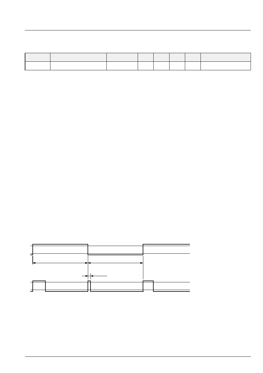
PRELIMINARY DATA SHEET
MAS 3506D
Micronas
41
4.6.3.2. Timing of PIO-Signals
Behavior of the FRAME signals
The BC-FRAME-TOGGLE toggles its level from '1' to
'0' and vice-versa every 432 ms. The BC-FRAME-
SYNC signal is set to '1' after the internal decoding
process for the Service Control Header has been fin-
ished for one frame. The signal could be used as an
interrupt input for the controller that triggers the read
out of the Service Control Header. As soon as the
MAS 3506D has recognized the corresponding read
command for the SCH, the BC-FRAME-SYNC is reset
before sending the first data word. The time t
read
depends on the response time of the controller. This
behavior reduces the possibility of not recognizing the
BC-FRAME-SYNC active state, if no controller inter-
rupt line is available for this purpose.
A similar behavior is implemented for MPEG-FRAME-
SYNC signal. However the frame period is restricted to
the MPEG frame length, the reset is initiated by issuing
a 'Read Ancillary MPEG Data' command.
Fig. 4≠16: Schematic timing of BC-FRAME signals
Table 4≠1: PIO Characteristics
Symbol
Parameter
Pin Name
Min.
Typ.
Max.
Unit
Test Conditions
t
BCTP
BC-frame toggle time
PI19
432
ms
V
h
V
L
432 ms
BC-FRAME-TOGGLE (PI 19)
432 ms
V
h
V
L
BC-FRAME-SYNC (PI13)
t
read
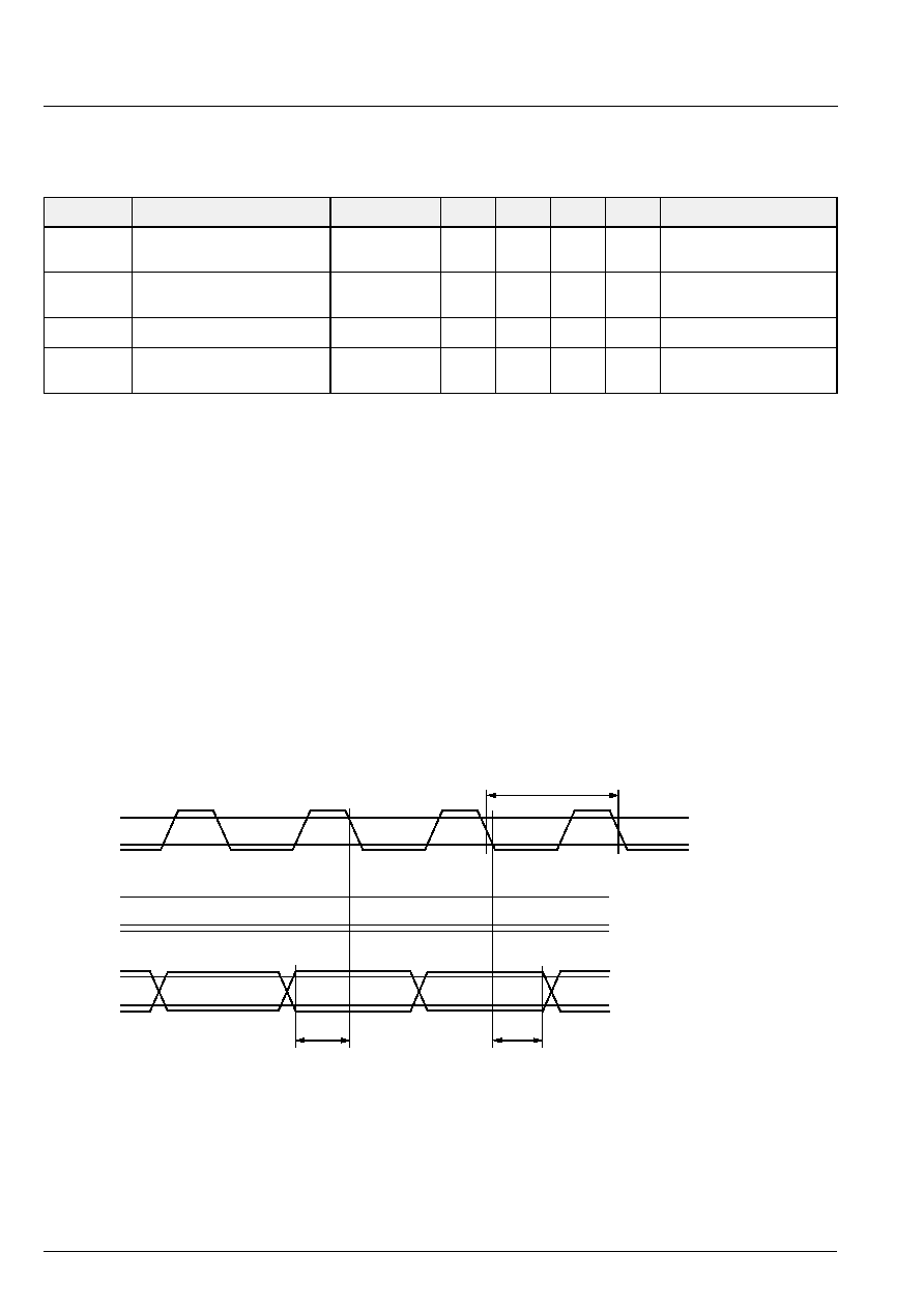
MAS 3506D
PRELIMINARY DATA SHEET
42
Micronas
4.6.3.3. I
2
S Bus Characteristics ≠ SDI
at T = T
A
, V
SUP
= 2.7 to 3.6 V, typ. values at T
A
= 27∞C, V
SUP
= 3.0 V, CLK
F
= 14.725 MHz, duty cycle = 50 %
Fig. 4≠17: Serial input
Symbol
Parameter
Pin Name
Min.
Typ.
Max.
Unit
Test Conditions
t
SICLK
I
2
S clock input clock period
SIC
480
ns
multimedia mode, mean
data rate < 150 kbit/s
t
SIIDS
I
2
S data setuptime before
falling edge of clock
SIC,
SID
50
t
SICLK
-
100
ns
t
SIIDH
I
2
S data hold time
SID
50
ns
t
bw
Burst wait time
SIC,
SID
480
H
L
H
L
H
L
T
SICLK
T
SIIDH
T
SIIDS
SIC
(SII)
SID
PRELIMINARY DATA SHEET
MAS 3506D
Micronas
43
4.6.3.4. I
2
S Characteristics ≠ SDO
at T = T
A
, V
SUP
= 2.7 to 3.6 V, typ. values at T
A
= 27∞C, V
SUP
= 3.0 V, CLK
F
= 14.725 MHz, duty cycle = 50 %
Fig. 4≠18: Serial output
4.6.3.5. Firmware Characteristics
at T = T
A
, V
SUP
= 2.7 to 3.6 V, typ. values at T
A
= 27∞C, V
SUP
= 3.0 V, CLK
F
= 14.725 MHz, duty cycle = 50 %
Symbol
Parameter
Pin Name
Min.
Typ.
Max.
Unit
Test Conditions
t
SOCLK
I
2
S clock output period
SOC
325
ns
48 kHz Stereo
32 bit/sample
t
SOISS
I
2
S wordstrobe delay time
after falling edge of clock
SOC,
SOI
0
ns
t
SOODC
I
2
S data delay time after
falling edge of clock
SOC,
SOD
0
ns
H
L
H
L
H
L
T
SOCLK
T
SOISS
T
SOISS
T
SOODC
SOC
SOI
SOD
Symbol
Parameter
Min.
Typ.
Max.
Unit
Test Conditions
Synchronization Times
t
bcsync
Synchronization on Broadcast Channel
216
432
ms
t
mpgsync
Synchronization on MPEG bit streams
12..36
72
ms
f
s
= 32 kHz, MPEG 2.5
Time constants
t
bcloop
Buffer controlled loop time constant (see Fig. 2≠
2 on page 8)
5
8
10
s
step response
t
anc
Validity of ancillary data after rising edge of
MPEG-FRAME-SYNC signal
6
ms
t
SCH
Validity of SCH-data after rising edge of
BC-FRAME-SYNC signal
400
ms
Ranges
PLLRange
Tracking range of sampling clock recovery PLL
-
200
200
ppm
MAS 3506D
PRELIMINARY DATA SHEET
44
Micronas
4.6.4. DC/DC Converter Characteristics
at T = T
A
, V
SUP
= 3.0 V, CLK
F
= 14.725 MHz, f
sw
= 230 kHz, typ. values at T
A
= +27 ∞C.
Unless otherwise noted: V
OUT
= 3.0 V, V
IN
= 1.2 V
Symbol
Parameter
Pin Name
Min.
Typ.
Max.
Unit
Test Conditions
V
IN1
Minimum start-up input voltage
1)
0.9
1.1
V
I
LOAD
= 0 mA
DCCF = $08000
(Reset)
V
IN2
Minimum operating input
voltage
1)
0.6
0.9
V
I
LOAD
= 55 mA,
DCCF = $08000
(Reset)
1.3
1.8
V
I
LOAD
= 250 mA,
DCCF = $08000
(Reset)
V
OUT
Output voltage range
Bits 16..14, Bit 9 of DCCF
Register (hex):
1C000
18000
14000
10000
0C000
08000
04000
00000
1C200
18200
14200
10200
0C200
08200
04200
00200
VSENS
3.567
3.460
3.354
3.248
3.144
3.039
2.935
2.831
2.729
2.625
2.524
2.422
2.321
2.219
2.118
2.017
V
VIN = 1.2 V
ILOAD = 50 mA
V
OTOL
Output voltage tolerance
VSENS
-
3.6
3.6
%
I
LOAD
= 50 mA
T
j
= 27
∞
C
V
IN
= 1.2 V
I
LOAD1
Output current
VSENS
150
mA
V
IN
= 0.9...1,5 V
I
LOAD2
250
mA
V
IN
= 1.8...3.0 V
dV
OUT
/dV
IN
/
V
OUT
Line regulation
VSENS
0.35
%/V
I
LOAD
= 50 mA
dV
OUT
/dV
IN
/
V
OUT
Line regulation
VSENS
0.7
%/V
I
LOAD
= 250 mA,
V
OUT
= 3.5 V,
V
IN
= 2.4 V
dV
OUT
/V
OUT
Load regulation
VSENS
-
0.5
%
I
LOAD
= 50...150 mA
dV
OUT
/V
OUT
Load regulation
VSENS
-
0.5
%
I
LOAD
= 50...250 mA,
V
OUT
= 3.5 V,
V
IN
= 2.4 V
PRELIMINARY DATA SHEET
MAS 3506D
Micronas
45
1)
All measurements are made with a C8 R/4L 20
µ
H, 25 m
ferrite ring-core coil, Zetex ZLMCS1000 Schottky
diode, and Sanyo/Oscon 6SA330M 330
µ
F, 25 m
ESR capacitors at input and output.
h
max
Maximum efficiency
90
%
V
IN
= 3.0 V,
V
OUT
= 3.5 V
I
SUPPLY
Supply current
VSENS
1.1
5
mA
V
IN
= 3.0 V, I
LOAD
= 0,
includ. switch current
I
L,MAX
Inductor current limit
DCSO,
DCSG
1.0
1.4
A
R
ON
Switch on-resistance
DCSO,
DCSG
0.4
I
LEAK
Switch leakage current
DCSO,
DCSG
0.1
1
µ
A
T
j
= 27
∞
C,
converter = off;
I
LOAD
= 0
µ
A
f
SW
Switch frequency
DCSO,
DCSG
156
230
460
kHz
Depending on DCCF
t
START
Start-up zime asserting to
PUP
DCEN
,
PUP
8
ms
V
IN
= 1.0 V,
I
LOAD
= 1 mA,
PUPLIM = 010 (Reset)
f
STARTUP
VSENSE
DCSO
250
kHz
VSENS < 1.9 V
Symbol
Parameter
Pin Name
Min.
Typ.
Max.
Unit
Test Conditions
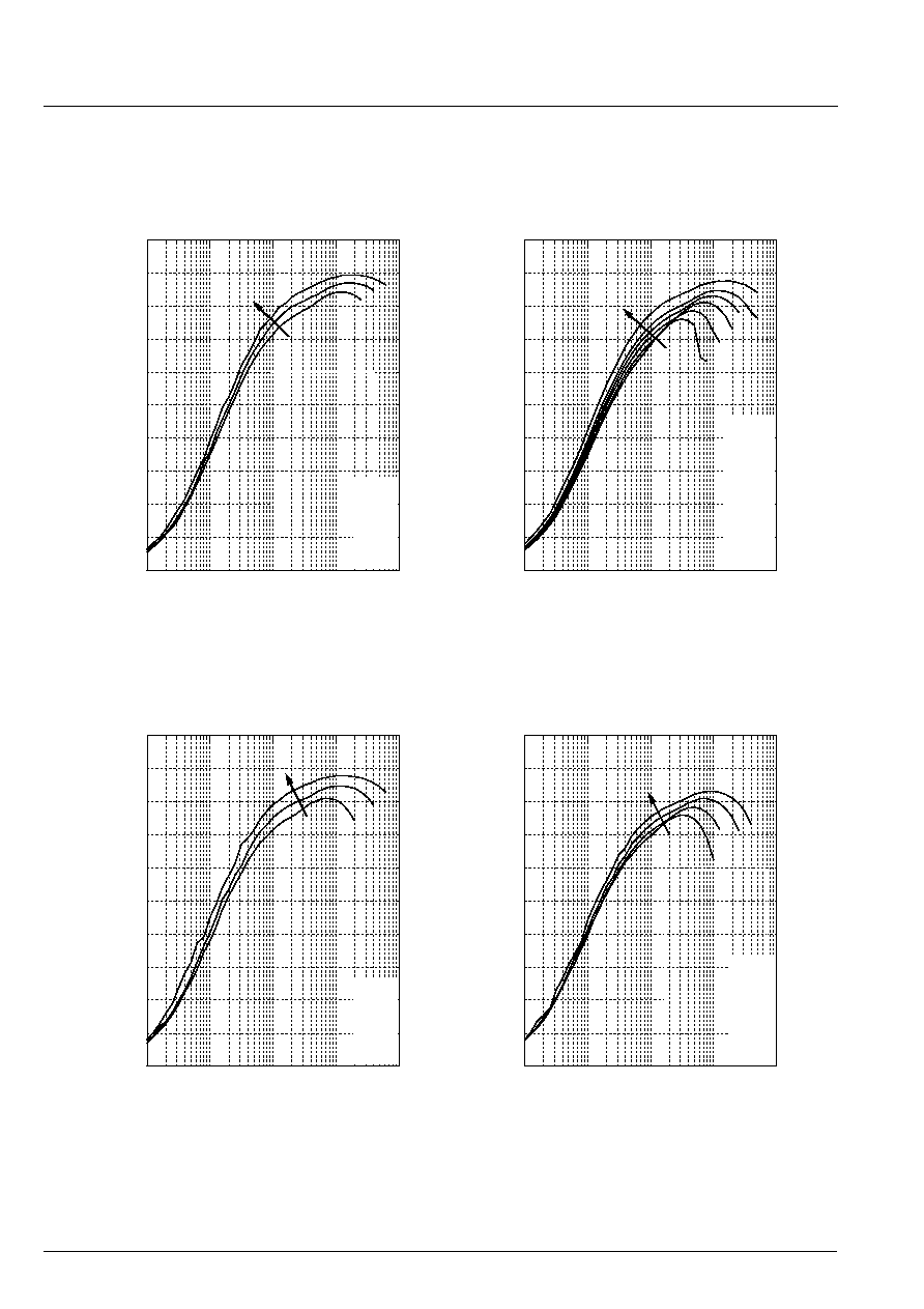
MAS 3506D
PRELIMINARY DATA SHEET
46
Micronas
4.6.5. Typical Performance Characteristics
Fig. 4≠19: Efficiency vs. Load Current
Load Current (A)
0
20
40
60
80
100
Efficiency (%)
Efficiency vs. Load Current
(Vout=2.7V)
Load Current (A)
0
20
40
60
80
100
Efficiency (%)
Efficiency vs. Load Current
(Vout=3.5V)
Load Current (A)
0
20
40
60
80
100
Efficiency (%)
Efficiency vs. Load Current
(Vout=2.2V)
Load Current (A)
0
20
40
60
80
100
Efficiency (%)
Efficiency vs. Load Current
(Vout=3.0V)
10
10
10
10
1
-4
-3
-2
-1
10
10
10
10
1
-4
-3
-2
-1
10
10
10
10
1
-4
-3
-2
-1
10
10
10
10
1
-4
-3
-2
-1
Vin:
2.4V
1.8V
1.5V
1.2V
0.9V
0.7V
Vin:
3.0V
2.4V
1.8V
Vin:
2.4V
1.8V
1.2V
Vin:
1.5V
1.2V
0.9V
0.7V
3.0 V
1.8 V
Vin
0.7 V
2.4 V
Vin
0.7 V
1.5 V
Vin
2.4 V
1.2 V
Vin
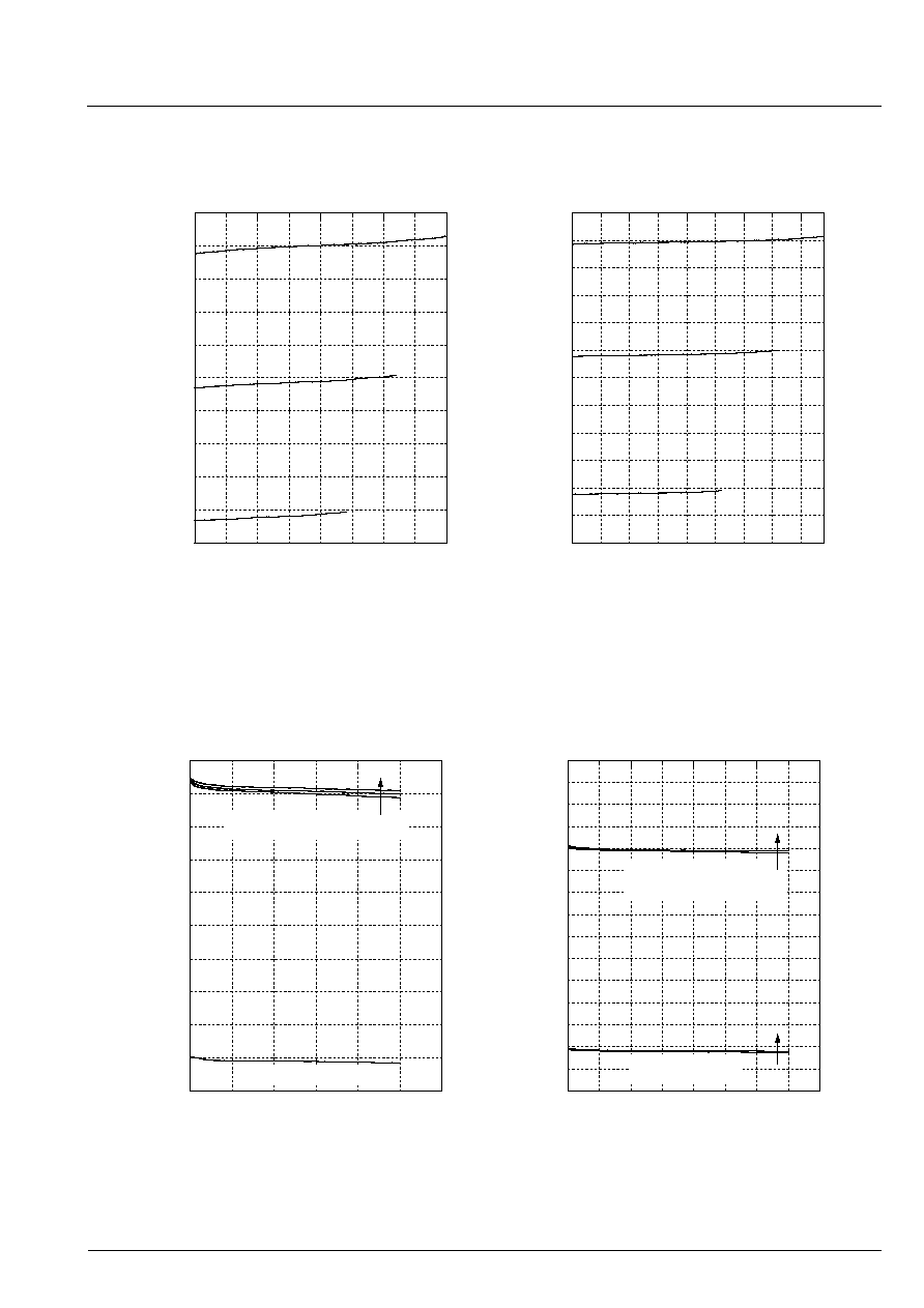
PRELIMINARY DATA SHEET
MAS 3506D
Micronas
47
Fig. 4≠20: Output Voltage vs. Input Voltage
Fig. 4≠21: Output Voltage vs. Load Current
1.5
2
2.5
3
3.5
Input Voltage (V)
2.6
2.8
3
3.2
3.4
3.6
Output Voltage (V)
Output Voltage vs. Input Voltage
Iload=250mA
0.9
1.4
1.9
2.4
2.9
Input Voltage (V)
2
2.2
2.4
2.6
2.8
3
3.2
Output Voltage (V)
Output Voltage vs. Input Voltage
Iload=50mA
3.5 V
3.1 V
2.7 V
3.1 V
2.2 V
2.7 V
0
0.1
0.2
0.3
Load Current (A)
2.6
2.8
3
3.2
3.4
3.6
Output Voltage (V)
Output Voltage
vs. Load Current
0
0.02
0.04
0.06
0.08
Load Current (A)
2
2.2
2.4
2.6
2.8
3
3.2
3.4
Output Voltage
Output Voltage
vs. Load Current
Vin=3V, 2.4V, 1.8V
Vin=2.4V
Vin=1.5V, 0.9V
Vin=1.5V, 0.9V
Vin
Vin
Vin
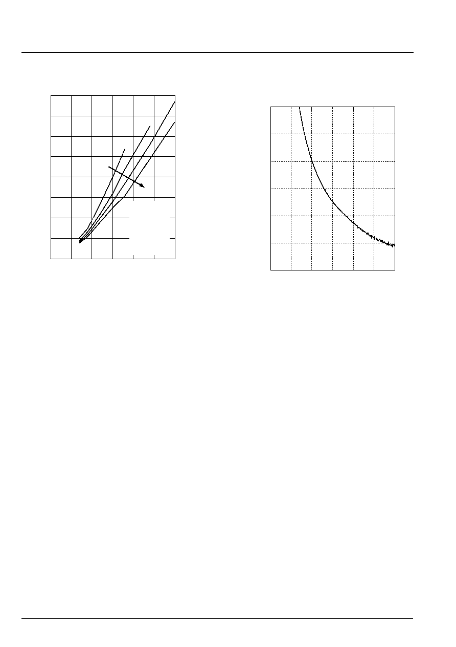
MAS 3506D
PRELIMINARY DATA SHEET
48
Micronas
Fig. 4≠22: Maximum Load Current vs. Input Voltage
Fig. 4≠23: No Load Supply Current vs. Input Voltage
0 1
2
3
Input Voltage (V)
0
0.2
0.4
0.6
0.8
Maximum Load Current (A)
Maximum Load Current
vs. Input Voltage
Vout=
3.5V
3.1V
2.7V
2.2V
3.5V
2.2V
V
out
0 1
2
3
Input Voltage (V)
0
2.0
4.0
6.0
No Load Supply Current
vs. Input Voltage
V
out
= 3 V
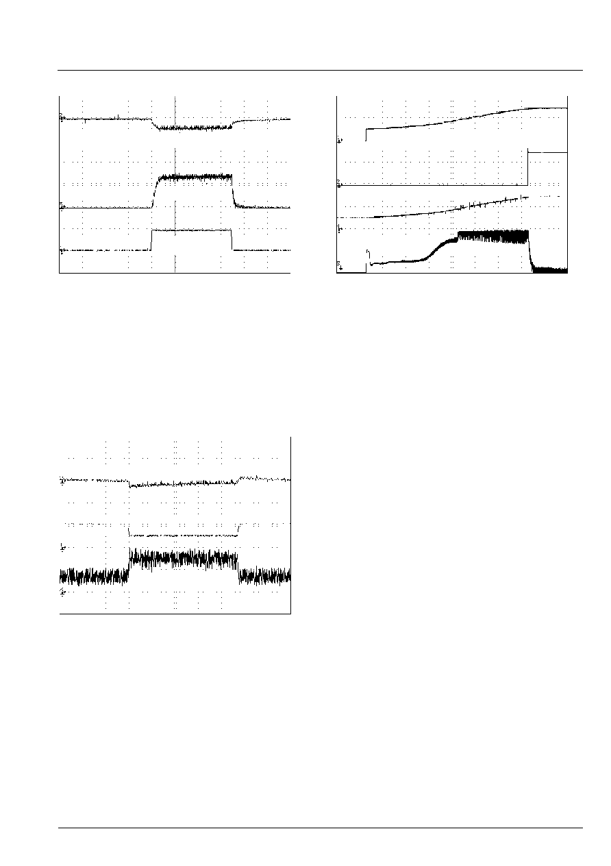
PRELIMINARY DATA SHEET
MAS 3506D
Micronas
49
Fig. 4≠24: Load Transient-Response
Fig. 4≠25: Line Transient-Response
Fig. 4≠26: Startup Waveform
500.00
µ
s/Div
V
in
= 1.2 V; V
out
= 3 V
1 Load Current
200.0 mA/Div
2 Output Voltage
100.0 mV/Div / AC-coupled
3 Inductor Current
500.0 mA/Div
3 V
0 A
0 A
I
load
= 100 mA; V
out
= 3 V
1 V
in
2.000 V/Div
2 Output Voltage
50.00 mV/Div / AC-coupled
3 Inductor Current 200.0 mA/Div
5.00 ms/Div
3 V
2 V
200
m
A
V
in
= 1 V; I
load
= 0 mA
1 V (DCEN)
2.000 V/Div
2 V (PUP)
2.000 V/Div
3 Inductor Current
500.0 mA/Div
4 Output Voltage
2.000 V/Div
500
µ
s/Div
0 A
3 V
3 V
3 V

MAS 3506D
PRELIMINARY DATA SHEET
50
Micronas

PRELIMINARY DATA SHEET
MAS 3506D
Micronas
51

All information and data contained in this data sheet are without any
commitment, are not to be considered as an offer for conclusion of a
contract, nor shall they be construed as to create any liability. Any new
issue of this data sheet invalidates previous issues. Product availability
and delivery are exclusively subject to our respective order confirmation
form; the same applies to orders based on development samples deliv-
ered. By this publication, Micronas GmbH does not assume responsibil-
ity for patent infringements or other rights of third parties which may
result from its use.
Further, Micronas GmbH reserves the right to revise this publication and
to make changes to its content, at any time, without obligation to notify
any person or entity of such revisions or changes.
No part of this publication may be reproduced, photocopied, stored on a
retrieval system, or transmitted without the express written consent of
Micronas GmbH.
MAS 3506D
PRELIMINARY DATA SHEET
52
Micronas
Micronas GmbH
Hans-Bunte-Strasse 19
D-79108 Freiburg (Germany)
P.O. Box 840
D-79008 Freiburg (Germany)
Tel. +49-761-517-0
Fax +49-761-517-2174
E-mail: docservice@micronas.com
Internet: www.micronas.com
Printed in Germany
Order No. 6251-433-1PD
5. Data Sheet History
1. Preliminary data sheet: "MAS 3506D WorldSpace
Broadcast Channel Audio Decoder, July 25, 2001,
6251-433-1PD. First release of the preliminary data
sheet.