 | –≠–ª–µ–∫—Ç—Ä–æ–Ω–Ω—ã–π –∫–æ–º–ø–æ–Ω–µ–Ω—Ç: MAS3507D | –°–∫–∞—á–∞—Ç—å:  PDF PDF  ZIP ZIP |
MAS 3507D
MPEG 1/2 Layer 2/3
Audio Decoder
Edition March 16, 2000
6251-459-3PD
PRELIMINARY DATA SHEET
MICRONAS

MAS 3507D
PRELIMINARY DATA SHEET
2
Micronas
Contents
Page
Section
Title
5
1.
Introduction
5
1.1.
Features
6
1.2.
Application Overview
6
1.2.1.
Multimedia Mode
6
1.2.2.
Broadcast Mode
7
2.
Functional Description of the MAS 3507D
7
2.1.
DSP Core
7
2.2.
Firmware (Internal Program ROM)
8
2.3.
Program Download Feature
8
2.4.
Baseband Processing
8
2.4.1.
Volume Control / Channel Mixer
8
2.4.2.
Mute / Bypass Tone Control
8
2.4.3.
Bass / Treble Control
9
2.5.
Clock Management
9
2.6.
Power Supply Concept
9
2.6.1.
Internal Voltage Monitor
9
2.6.2.
DC/DC Converter
9
2.6.3.
Stand-by Functions
10
2.6.4.
Start-up Sequence
11
2.7.
Interfaces
11
2.7.1.
MPEG Bit Stream Interface (SDI)
11
2.7.2.
SDI* Selection
12
2.7.3.
Parallel Input Output Interface (PIO)
12
2.7.3.1.
PIO-DMA Input Mode
12
2.7.3.2.
Writing MPEG Data to the PIO-DMA
13
2.7.3.3.
DMA Handshake Protocol
13
2.7.3.4.
End of DMA Transfer
13
2.7.4.
Audio Output Interface (SDO)
13
2.7.4.1.
Mode 1: 16 Bits/Sample(I
2
S Compatible Data Format)
14
2.7.4.2.
Mode 2:32 Bit/Sample (Inverted SOI)
14
2.7.4.3.
Other Output Modes
15
2.8.
Start-up Configuration
15
2.8.1.
Parallel Input Output Interface (PIO)
16
2.9.
Status Pins in SDI Input Mode

Contents, continued
Page
Section
Title
PRELIMINARY DATA SHEET
MAS 3507D
Micronas
3
18
3.
Control Interfaces
18
3.1.
I
2
C Bus Interface
18
3.1.1.
Device and Subaddresses
19
3.2.
Command Structure
19
3.2.1.
The Internal Fixed Point Number Format
20
3.2.2.
Conventions for the Command Description
20
3.3.
Detailed MAS 3507D Command Syntax
20
3.3.1.
Run
21
3.3.2.
Read Control Interface Data
21
3.3.3.
Write Register
21
3.3.4.
Write D0 Memory
21
3.3.5.
Write D1 Memory
22
3.3.6.
Read Register
22
3.3.7.
Read D0 Memory
22
3.3.8.
Read D1 Memory
22
3.3.9.
Default Read
23
3.4.
Protocol Description
23
3.4.1.
Run Command
23
3.4.2.
Read Control Interface Data
23
3.4.3.
Write to MAS 3507D Register
23
3.4.4.
Write to MAS 3507D D0 Memory
24
3.4.5.
Write to MAS 3507D D1 Memory
24
3.4.6.
Read Register
24
3.4.7.
Read D0 memory
24
3.4.8.
Read D1 memory
25
3.4.9.
Default Read
25
3.4.10.
Write Data to the Control Register
25
3.5.
Version Number
26
3.6.
Register Table
26
3.6.1.
DC/DC Converter
28
3.6.2.
Muting / Bypass Tone Control
28
3.6.3.
Bass and Treble Control
30
3.7.
Memory Area
30
3.7.1.
Status Memory
30
3.7.1.1.
MPEG Frame Counter
31
3.7.1.2.
MPEG Status 1
32
3.7.1.3.
MPEG Status 2
33
3.7.1.4.
CRC Error Counter
33
3.7.1.5.
Number Of Ancillary Bits
34
3.7.1.6.
Ancillary Data
35
3.7.2.
Configuration Memory
36
3.7.2.1.
PLL Offset for 44/48 kHz Sampling Frequency
37
3.7.2.2.
Output Configuration
37
3.7.3.
Baseband Volume Matrix

MAS 3507D
PRELIMINARY DATA SHEET
4
Micronas
Contents, continued
Page
Section
Title
39
4.
Specifications
39
4.1.
Outline Dimensions
40
4.2.
Pin Connections and Short Descriptions
43
4.2.1.
Pin Descriptions
43
4.2.1.1.
Power Supply Pins
43
4.2.1.2.
DC/DC Converter Pins
43
4.2.1.3.
Control Lines
43
4.2.1.4.
Parallel Interface Lines
43
4.2.1.4.1.
PIO Handshake Lines
43
4.2.1.4.2.
PIO Data Lines
44
4.2.1.5.
Voltage Supervision And Other Functions
44
4.2.1.6.
Serial Input Interface
44
4.2.1.7.
Serial Output Interface
45
4.2.1.8.
Miscellaneous
45
4.2.2.
Pin Configurations
46
4.2.3.
Internal Pin Circuits
47
4.2.4.
Electrical Characteristics
47
4.2.4.1.
Absolute Maximum Ratings
47
4.2.4.2.
Recommended Operating Conditions
49
4.2.4.3.
Characteristics
50
4.2.4.3.1.
I
2
C Characteristics
51
4.2.4.3.2.
I
2
S Bus Characteristics ≠ SDI
52
4.2.4.3.3.
I
2
S Characteristics ≠ SDO
53
4.2.4.4.
Firmware Characteristics
53
4.2.4.4.1.
Input Timing Parameters of the MultimediaMode
54
4.2.4.5.
DC/DC Converter Characteristics
55
4.2.4.6.
Typical Performance Characteristics
60
5.
Data Sheet History

PRELIMINARY DATA SHEET
MAS 3507D
Micronas
5
MPEG 1/2 Layer 2/3 Audio Decoder
Release Note: Revision bars indicate significant
changes to the previous edition.
This data sheet applies to MAS 3507D version G10
and following versions.
1. Introduction
The MAS 3507D is a single-chip MPEG layer 2/3 audio
decoder for use in audio broadcast or memory-based
playback applications. Due to embedded memories,
the embedded DC/DC up-converter, and the very low
power consumption, the MAS 3507D is ideally suited
for portable electronics.
In MPEG 1 (ISO 11172-3), three hierarchical layers of
compression have been standardized. The most
sophisticated and complex, layer 3, allows compres-
sion rates of approximately 12:1 for mono and stereo
signals while still maintaining CD audio quality. Layer 2
(widely used in DVB, ADR, and DAB) achieves a com-
pression of 8:1 providing CD quality.
In order to achieve better audio quality at low bit rates
(<64 kbit/s per audio channel), three additional sam-
pling frequencies are provided by MPEG 2
(ISO 13818-3). The MAS 3507D decodes both layer 2
and layer 3 bit streams as defined in MPEG 1 and 2.
The multichannel/multilingual capabilities defined by
MPEG 2 are not supported by the MAS 3507D. An
extension to the MPEG 2 layer 3 standard developed
by FhG Erlangen, Germany sometimes referenced as
MPEG 2.5, for extremely low bit rates at sampling fre-
quencies of 12, 11.025, or 8 kHz is also supported by
the MAS 3507D.
1.1. Features
≠ Serial asynchronous MPEG bit stream input (SDI)
≠ Parallel (PIO-DMA) Input
≠ Broadcast and multimedia operation mode
≠ Automatic locking to given data rate in broadcast
mode
≠ Data request triggered by 'demand signal' in multi-
media mode
≠ Output audio data delivered (in various formats) via
an I
2
S bus (SDO)
≠ Digital volume / stereo channel mixer / Bass / Treble
≠ Output sampling clocks are generated and con-
trolled internally.
≠ Ancillary data provided via I
2
C interface
≠ Status information accessible via PIO pins or I
2
C
≠ "CRC Error" and "MPEG Frame Synchronization"
Indicators at Pins in serial input mode
≠ Power management for reduced power consumption
at lower sampling frequencies
≠ Low power dissipation (30 mW @ f
s
12 kHz,
46 mW @ f
s
24 kHz, 86 mW @ f
s
> 24 kHz @
2.7 V)
≠ Supply voltage range: 1.0 V to 3.6 V due to built-in
DC/DC converter (1-cell/2-cell battery operation)
≠ Adjustable power supply supervision
≠ Power-off function
≠ Additional functionality achievable via download
software (CELP voice Decoder, ADPCM encoder /
decoder)
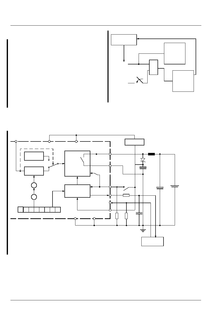
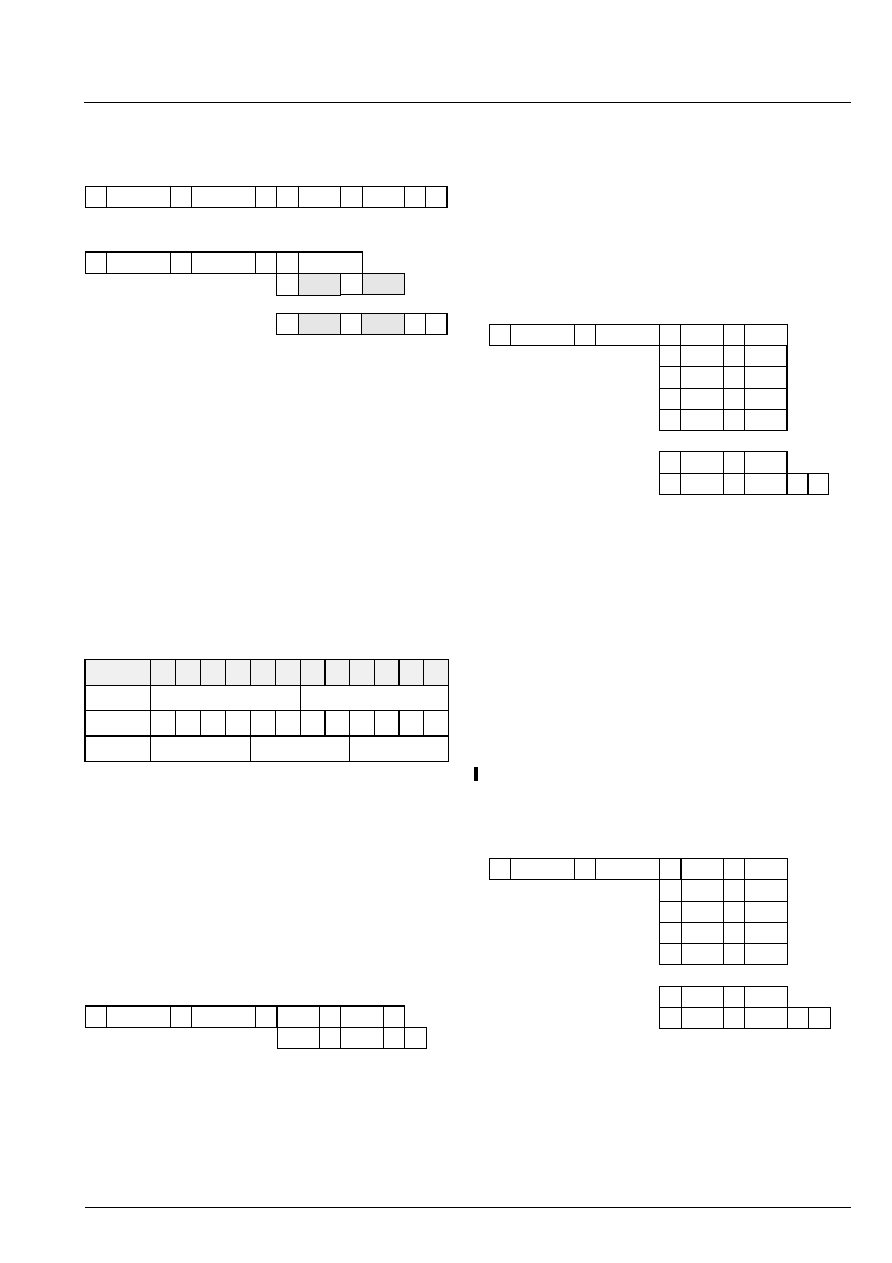
Fig. 1≠1: MAS 3507D block diagram
CLKI
CLKO
decoded output
MPEG 1/2
audio bit stream
/3/
/2/
Clock
Synthesizer
Serial Out
I
2
S
Serial In
I
2
C
RISC DSP Core
MPEG frame sync
CRC error
PIO
DC/DC
Converter
/3/
/8+5/
/2/
serial control
MAS 3507D
MAS 3507D
PRELIMINARY DATA SHEET
6
Micronas
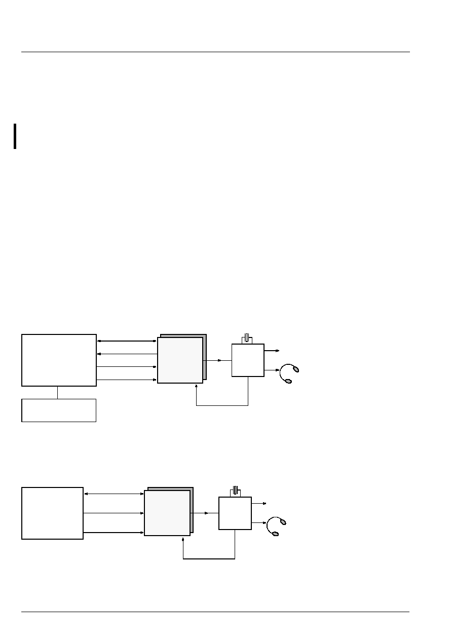
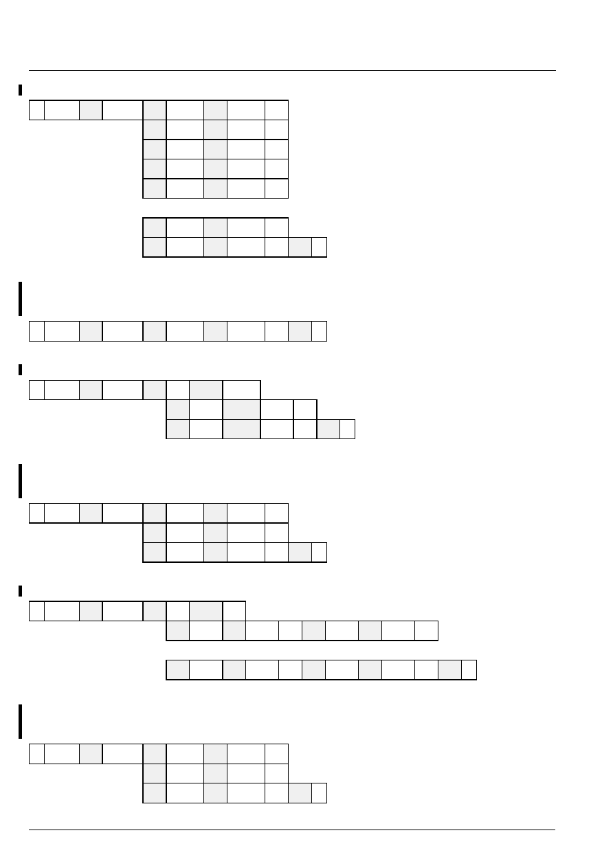
1.2. Application Overview
The MAS 3507D can be applied in two major environ-
ments: in multimedia mode or in broadcast mode. For
both modes, the DAC 3550A fits perfectly to the
requirements of the MAS 3507D. It is a high-quality
multi sample rate DAC (8 kHz ... 50 kHz) with internal
crystal oscillator, which is only needed for generating
the decoder clock, and integrated stereo headphone
amplifier plus 2 stereo inputs.
1.2.1. Multimedia Mode
In a memory-based multimedia environment, the easi-
est way to incorporate a MAS 3507D decoder is to use
its data-demand pin. This pin can be used directly to
request input bit stream data from the host or memory
system.
While the demand pin is active, the data stream shall
be transmitted to the MAS 3507D. The bit stream clock
should be higher than the actual data rate of the
MPEG bit stream (1 MHz bit stream clock works with
all MPEG bit rates). The demand signal will be active
until the input buffer of the MAS 3507D is filled.
A delayed response of the host to the demand signal
(by several milliseconds) or an interrupted response of
the host will be tolerated by the MAS 3507D as long as
the input buffer does not run empty. A PC might use its
DMA capabilities to transfer the data in the background
to the MAS 3507D without interfering with its fore-
ground processes.
The source of the bit stream may be a memory (e.g.
ROM, Flash) or PC peripherals, such as CD-ROM
drive, an ISDN card, a hard disk or a floppy disk drive.
1.2.2. Broadcast Mode
In environments where the bit stream is delivered from
an independent transmitter to one or more receivers,
the MAS 3507D cannot act as master for the bit
stream clock. In this mode, it synchronizes itself to the
incoming bit stream data rate by a digital PLL and gen-
erates a synchronized digital audio sample clock for
the required output sample rates.
Fig. 1≠2: Block diagram of a MAS 3507D, decoding a stored bit stream in multimedia mode
Fig. 1≠3: Block diagram of a MAS 3507D in a broadcast environment
MAS 3507D
ROM, CD-ROM,
RAM, Flash Mem. ..
DAC
Host
3550A
(PC, Controller)
I
2
S
line out
I
2
C
demand signal
demand clock
MPEG bit stream
CLKI
CLKOUT
14.725 MHz
MAS 3507D
DAC
Receiver
3550A
Front-end
I
2
S
line out
CLKI
control I
2
C
L3 bit stream
(fixed rate)
clock
14.725 MHz
CLKOUT
PRELIMINARY DATA SHEET
MAS 3507D
Micronas
7
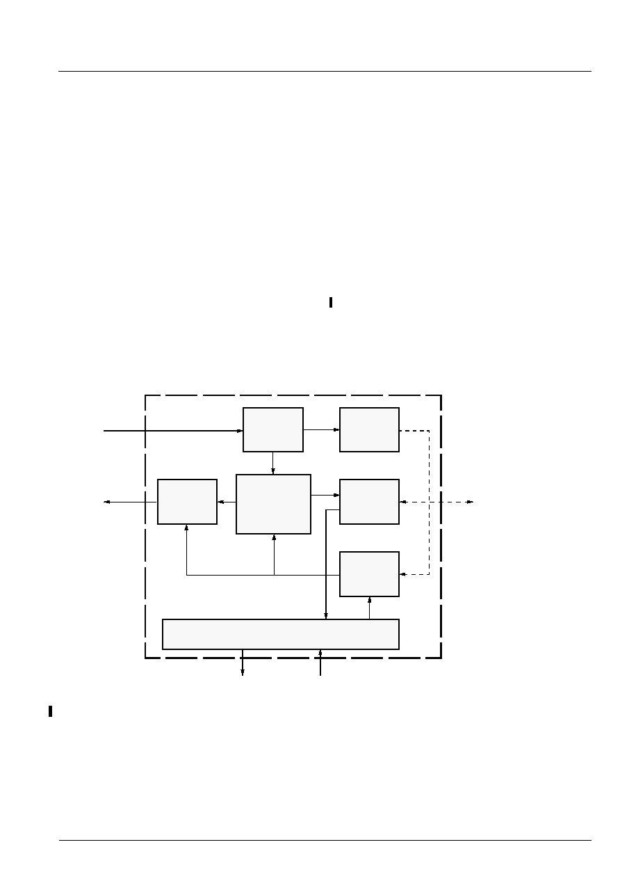
2. Functional Description of the MAS 3507D
2.1. DSP Core
The hardware of the MAS 3507D consists of a high
performance RISC Digital Signal Processor (DSP) and
appropriate interfaces (see Fig. 2≠1). The internal pro-
cessor works with a memory word length of 20 bits
and an extended range of 32 bits in its accumulators.
The instruction set of the DSP is highly optimized for
audio data compression and decompression. Thus,
only very small areas of internal RAM and ROM are
required. All data input and output actions are based
on a `non cycle stealing' background DMA that does
not cause any computational overhead.
2.2. Firmware (Internal Program ROM)
A valid MPEG 1/2/2.5 layer 2/3 data signal is taken as
input. The signal lines are a clock line SIC
and the data
line SID. The MPEG decoder performs the audio
decoding. The steps for decoding are
≠ synchronization,
≠ side information extraction,
≠ audio data decoding,
≠ ancillary data extraction, and
≠ volume and tone control.
For the supported bit rates and sample rates, see
Table 3≠12 on page 32. Frame synchronization and
CRC-error signals are provided at the output pins of
the MAS 3507D in serial input mode.
Fig. 2≠1: Block diagram of the MPEG Decoder in serial input mode
Sync
Ancillary
MPEG
Decoder
to
µ
C
MPEG Bit Stream
Digital Audio Output
Data
Decoder
Status
Config. Reg.
PIO
Status
Start-up Config.
Volume
Tone
Control
MAS 3507D
PRELIMINARY DATA SHEET
8
Micronas
2.3. Program Download Feature
This is an additional feature that is not required for the
MPEG decoding function.
The overall function of the MAS 3507D can be altered
by downloading up to 1 kWord program code into the
internal RAM and executing this code instead of the
ROM code. During this time, MPEG decoding is not
possible.
The code must be downloaded by the `write to mem-
ory' command (see Section 3.3.) into an area of RAM
that is switchable from data memory to program mem-
ory. A `run' command (see Section 3.3.1.) starts the
operation.
Micronas provides modules for voice-decoding using
the CELP algorithm (performing good speech quality
at very low bit rates) and for encoding and decoding
audio data with ADPCM.
Detailed information about downloading is provided in
combination with the MAS 3507D software develop-
ment package from Micronas.
For commercial issues and detailed information please
contact our sales department.
2.4. Baseband Processing
2.4.1. Volume Control / Channel Mixer
A digital volume control matrix is applied to the digital
stereo audio data. This performs additional balance
control and a simple kind of stereo basewidth
enhancement. The 4 factors LL, LR, RL, and RR are
adjustable via the controller with 20-bit resolution. See
Fig. 3≠2 and Section 3.7.3. for details.
2.4.2. Mute / Bypass Tone Control
A special bit enables a fast and simple mute functional-
ity without changing the current volume setting.
Another bit allows to bypass the complete bass / treble
/ volume control. See for details Section 3.6.2.
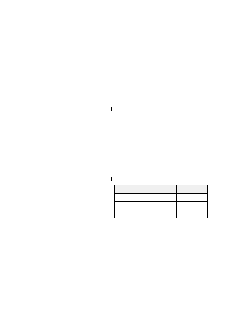
2.4.3. Bass / Treble Control
Tone control is implemented in the MAS 3507D. It
allows the control of bass and treble in a range up to
±15 dB, as Table 3≠9 shows. To prevent overflow or
clipping effects, the prescaler is built-in. The prescaler
decreases the overall gain of the tone filter, so the full
range up to +15 dB is usable without clipping.
Due to the different frequency ranges in MPEG 1,
MPEG 2, or MPEG 2.5, the bass cutoff frequencies dif-
fer.
For details see Section 3.6.3..
Table 2≠1: Cutoff Frequencies
Cutoff
Bass
Treble
MPEG 1
100 Hz
10 kHz
MPEG 2
200 Hz
10 kHz
MPEG 2.5
400 Hz
10 kHz
PRELIMINARY DATA SHEET
MAS 3507D
Micronas
9
2.5. Clock Management
The MAS 3507D should be driven by a single clock at
a frequency of 14.725 MHz. It is possible to drive the
MAS 3507D with other reference clocks (see Section
3.7.2.1. on page 36).
The CLKI signal acts as a reference for the embedded
clock synthesizer that generates the internal system
clock. Based on the reference input clock CLKI
,
a syn-
chronized output clock CLKO
that depends on the
audio sample frequency of the decompressed bit
stream is generated and provided as `master clock' to
external D/A converters. Some of them need master
clocks that have a fixed relation to the sampling fre-
quencies. A scaler can be switched on during start-up,
optionally, by setting the PI8 pin to 0. Then, the clock-out
will automatically be divided by 1, 2, or 4 as defined in
Table 2≠2.
2.6. Power Supply Concept
The MAS 3507D offers an embedded controlled DC/
DC converter for battery based power supply con-
cepts. It works as an up-converter.
2.6.1. Internal Voltage Monitor
An internal voltage monitor compares the input voltage
at the VSENS
pin with an internal reference value that
is adjustable via I
2
C bus. The PUP output pin becomes
inactive when the voltage at the VSENS pin drops
below the programmed value of the reference voltage.
It is important that the WSEN must not be activated
before the PUP is generated. The PUP signal thresh-
olds are listed in Table 3≠8. The internal voltage moni-
tor will be activated with a high level at Pin DCEN.
2.6.2. DC/DC Converter
The DC/DC converter of the MAS 3507D is used to
generate a fixed power supply voltage even if the chip
set is powered by battery cells in portable applications.
The DC/DC converter is designed for the application of
1 or 2 batteries or NiCd cells as shown in Fig. 2≠3
which shows the standard application circuit. The DC/
DC converter is switched on by activating the DCEN
pin. Its output power is sufficient for other ICs as well.
Note: Connecting DCEN directly to VDD leads to
unexpected states of the DCCF register.
The PUP signal should be read out by the system con-
troller.
A 22
µ
H inductor is required for the application. The
important specification item is the inductor saturation
current rating, which should be greater than 2.5 times
the DC load current. The DC resistance of the inductor
is important for efficiency. The primary criterion for
selecting the output filter capacitor is low equivalent
series resistance (ESR), as the product of the inductor
current variation and the ESR determines the high-fre-
quency amplitude seen on the output voltage. The
Schottky diode should have a low voltage drop V
D
for a
high overall efficiency of the DC/DC converter. The
current rating of the diode should also be greater than
2.5 times the DC output current. The VSENS pin has
to be always connected to the output voltage.
2.6.3. Stand-by Functions
The digital part of the MAS 3507D and the DC/DC
converter are turned on by setting WSEN. If only the
DC/DC converter should work, it can remain active by
setting DCEN alone to supply other parts of the appli-
cation even if the audio decoding part of the
MAS 3507D is not being used. The WSEN power-up
pin of the digital part may be handled by the controller.
Please pay attention to the fact, that I
2
C protocol is
working only if the processor and its interfaces works
(WSEN = 1)
Table 2≠2: CLKO Frequencies
f
s
/kHz
CLKO/MHz
scaler on
CLKO/MHz
scaler off
48, 32
24.576
24.576
44.1
22.5792
22.5792
24, 16
12.288
24.576
22.05
11.2896
22.5792
12, 8
6.144
24.576
11.025
5.6448
22.5792
MAS 3507D
PRELIMINARY DATA SHEET
10
Micronas
2.6.4. Start-up Sequence
The DC/DC converter starts from a minimum input
voltage of 0.9 V. There should be no output load during
startup. In case WSEN is active, the MAS 3507D is in
the DSP operation mode. The start-up script should be
as follows:
1. Enable the DC/DC-converter with a high signal
(VDD, AVDD) at pin DCEN.
2. Wait until PUP goes "high".
3. Wait one more millisecond to guarantee that the out-
put voltage has settled (recommended).
4. Enable the MAS 3507D with a "high" signal at pin
"WSEN".
Please also refer to Figure 2≠2.
Fig. 2≠2: DC/DC operation
Fig. 2≠3: DC/DC converter connections
> 0.9 V
WSEN > 2 V
DCEN
=1
DSP
operation
µController
DC/DC
On
button
voltage monitor
DC/DC
converter
Start-up
oscillator
Frequency
divider
optional
filter
x2
+32
0...15
32...47
64...94
10
16
-
+
-
+
VSS
AVSS
AVDD
VDD
CLKI
DCSO
DCSG
DCEN
PUP
WSEN
VSENSE
V
in
0.9 V
22
µ
H
C
out
330
µ
F
Low ESR
C
in
330
µ
F
DCCF
$8e
9
47 k
µController
47 k
Power-On
Push Button
10 k
10 nF

PRELIMINARY DATA SHEET
MAS 3507D
Micronas
11
2.7. Interfaces
The MAS 3507D uses an I
2
C control interface,
2 selectable serial input interfaces for MPEG bit
stream (SDI, SDI*) , a parallel I/O interface (PIO) for
MPEG- or ADPCM-data and a digital audio output
interface (SDO) for the decoded audio data (I
2
S or
similar). Additionally, the parallel I/O interface (PIO)
may be used for monitoring and mode selection tasks.
The PIO lines are defined by the internal firmware.
2.7.1. MPEG Bit Stream Interface (SDI)
The MPEG bit stream input interface uses the three
pins: SIC,
SII
, and SID. For MPEG decoding operation,
the SII pin must always be connected to VSS.
The serial interface has to be initialized before the
first use. Otherwise no output signal is produced.
After Power-up or a rising slope on Pin PORQ, write
the following I
2
C-command, while SIC is hold low:
W $3A 68 93 B0 00 02
(write $0020 into register $3B)
W $3A 68 00 01
(execute "RUN 1" command)
The MPEG input signal format is shown in Fig. 2≠4.
The data values are latched with the falling edge of the
SIC signal.
The MPEG bit stream generated by an encoder is
unformatted. It will be formatted (e.g. 8 bit or 16 bit) by
storing on a media (Flash-RAM, Harddisk). The serial
data required from the MPEG bit stream interface must
be in the same bit order as produced by the encoder.
2.7.2. SDI* Selection
An alternative serial input (SDI*) is available. The alter-
native serial input can be selected by setting register
SI1M0 at address $4f (see Table 2≠3).
Fig. 2≠4: Schematic timing of the SDI (MPEG) input
Table 2≠3: SDI* Selection via Register SI1M0,
$4f (write)
Value
Function
0
use SDI lines
2
use PI14...PI16 pins for
serial input (named SDI*)
SIC
SII
SID
V
h
V
l
V
h
V
l
V
h
V
l
data valid
latch data at falling edge of clock
MAS 3507D
PRELIMINARY DATA SHEET
12
Micronas
2.7.3. Parallel Input Output Interface (PIO)
The parallel interface of the MAS 3507D uses the lines
PI0...PI4, PI8, PI12...PI19, and several control lines.
2.7.3.1. PIO-DMA Input Mode
By setting the PIO pin PI4 to "1", the PIO-DMA input
mode of the MAS 3507D is activated after reset.
Normally, the input mode should not be altered in a
customer's application. Should this nonetheless be
desired, the necessary changes are described in
Table 2≠4 and Table 2≠5.
2.7.3.2. Writing MPEG Data to the PIO-DMA
The PIO-DMA mode enables the writing of 8-bit paral-
lel MPEG data to the MAS 3507D. In this mode, PIO
lines PI19...PI12 are switched to the MAS 3507D data
input which hence will be an 8-bit parallel input port
with MSB first (at position PI19) for the MPEG bit
stream data. In order to write data to this parallel port
successfully, a special handshake protocol has to be
used by the controller (see Fig. 2≠5).
Note: Either SII has to be set to "1", or SIC clock input
has to be stopped ("0") in this mode.
.
.
Fig. 2≠5: Handshake protocol for writing MPEG data to the PIO-DMA
Table 2≠4: Switching from SDI- to PIO-DMA-Input
Address
1)
Value
$e6, Bit 4
1
1)
Startup Configuration Register
Table 2≠5: Switching from PIO-DMA- to SDI-Input
Step
Address
1)
Value
1
$e6, Bit 4
0
2
$4b
$82
1)
PIO Configuration Register
Note: These 2 steps must be done in above
order!
EOD
PR
RTR
PI[19:12]
high
low
high
low
high
low
high
low
t
st
t
rpr
t
rtrq
t
set
t
h
t
r
t
pr
t
pd
t
eodq
t
eod
Byte 15
Byte 1
MAS 3507D latches the PIO DATA

PRELIMINARY DATA SHEET
MAS 3507D
Micronas
13
2.7.3.3. DMA Handshake Protocol
The data transfer can be started after the EOD pin of
the MAS 3507D is set to "high". After verifying this, the
controller signalizes the sending of data by activating
the PR line. The MAS 3507D responds by setting the
RTR line to the "low" level. The MAS 3507D reads the
data PI[19:12] t
pd
ns after rising edge of the PR. The
next data word write operation will again be initialized
by setting the PR line via the controller. Please refer to
Figure 2≠5 and Table 2≠6 for the exact timing
2.7.3.4. End of DMA Transfer
The above procedure will be repeated until the
MAS 3507D sets the EOD signal to "0", which indi-
cates that the transfer of one data block has been exe-
cuted. Subsequently, the controller should set PR to
"0", wait until EOD rises again, and then repeat the
procedure (see Section 2.7.3.3. ) to send the next
block of data. The DMA buffer is 15 bytes long.
The recommended PIO-DMA conditions and the char-
acteristics of the PIO timing are given in Table 2≠6
2.7.4. Audio Output Interface (SDO)
The audio output interface of the MAS 3507D is a
standard I
2
S interface. It is possible to choose between
two standard interfaces (16 bit with delay or 32 bit with-
out delay and inverted SOI) via start-up configuration.
These setup modes meet the performance of the most
common DACs. It is also possible to select other inter-
face modes via I
2
C commands (see Section 2.7.4.3.).
2.7.4.1. Mode 1: 16 Bits/Sample
(I
2
S Compatible Data Format)
A schematic timing diagram of the SDO interface in
16 bit/sample mode is shown in Fig. 2≠6.
.
Fig. 2≠6: Schematic timing of the SDO interface in 16 bit/sample mode
Table 2≠6: PIO DMA Timing
Symbol
PIO Pin
Min.
Max.
Unit
t
st
PR, EOD
0.010
2000
µ
s
t
r
PR, RTR
40
160
ns
t
pd
PR,
PI[19:12]
120
480
ns
t
set
PI[19:12]
160
no limit
ns
t
h
PI[19:12]
160
no limit
ns
t
rtrq
RTR
200
30000
ns
t
pr
PR
120
no limit
ns
t
rpr
PR, RTR
40
no limit
ns
t
eod
PR, EOD
40
160
ns
t
eodq
EOD
0
500
µ
s
SOC
SOD
V
h
V
l
SOI
left 16-bit audio sample
right 16-bit audio sample
15 14 13 12 11 10 9
8
7
6
5
4
3
2
1
0
13 12 11 10
9 8
7
6
5
4
3
2
1
0
15 14
V
h
V
l
V
h
V
l

MAS 3507D
PRELIMINARY DATA SHEET
14
Micronas
2.7.4.2. Mode 2:32 Bit/Sample (Inverted SOI)
If the serial output generates 32 bits per audio sample,
only the first 20 bits will carry valid audio data. The 12
trailing bits are set to zero by default (see Fig. 2≠7)
The 12 trailing bits for left and right channel of the SDO
interface can be accessed by writing to registers as
shown in Table 2≠7.
2.7.4.3. Other Output Modes
The interface is also configurable by software to work
in different modes. It is possible to choose:
≠ 16 or 32 bit/sample modes,
≠ inverted or noninverted word strobe (SOI),
≠ no delay or delay of data related to word strobe
≠ inverted or noninverted I
2
S-Clock (SOC).
For further details see Section 3.7.2.2.
Fig. 2≠7: Schematic timing of the SDO interface in 32 bit/sample mode
Table 2≠7: Access for Trailing Bits
Register
Bit 0 ... 11
$c5
Left Channel
$c6
Right Channel
30 29 28 27 26 25 ... 7
6
5
4
3
2
1
0
31 30 29 28 27 26 25
7
6
5
4
3
2
1
0
left 32-bit audio sample
right 32-bit audio sample
SOC
SOD
SOI
V
h
V
l
V
h
V
l
V
h
V
l
...
...
31
...
PRELIMINARY DATA SHEET
MAS 3507D
Micronas
15
2.8. Start-up Configuration
Basic operation of the MAS 3507D is possible without
controller interaction. Configuration and the most
important status information are available by the PIO
interface. The start-up configuration is selected
according to the levels of several PIO pins. The levels
should be set via high impedance resistors (for exam-
ple 10 k
)
to VSS or VDD and will be copied into the
StartupConfig register directly after power up / reset.
After start-up, the PIO will be reconfigured as output.
To enable greater flexibility, it is possible to configure
the MAS 3507D without using the PIO pins or to recon-
figure the IC after start-up. The procedure for this is to
send two I
2
C commands to the MAS 3507D:
≠ Writing the StartupConfig register (see Section 3.6.
on page 26)
≠ Execute a `run $0fcd' command (see
Section 3.3.1.).
The configuration will be active up to a reset. Then, the
new configuration will be loaded again via PIO.
2.8.1. Parallel Input Output Interface (PIO)
During start-up, the PIO will read the start-up configu-
ration. This is to define the environment for the
MAS 3507D. The following pins must be connected via
resistors to VSS or VDD:
Table 2≠8: Start-up configuration
1)
1) Start-up setting can be changed by I
2
C commands
after reset.
PIO
Pin
"0"
"1"
PI8
divide CLKO by 1,
2, or 4 (according
to MPEG 1, 2, or
2.5)
CLKO fixed at
24.576 or
22.5792 MHz
PI4
SDI input mode
PIO-DMA input
mode
PI3
Enable layer 3
Disable layer 3
PI2
Enable layer 2
Disable layer 2
PI1
SDO output: 32 bit
SDO output: 16 bit
PI0
input: Multimedia
mode (PLL off)
input: Broadcast
mode (PLL on)
MAS 3507D
PRELIMINARY DATA SHEET
16
Micronas
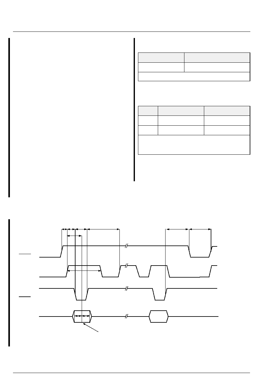
2.9. Status Pins in SDI Input Mode
After having read the start-up configuration, the PIO
will be switched to `
µ
P-mode'. In
µ
P-mode, the addi-
tional PIO control lines (PR, PCS
)
are evaluated. If the
MPEG decoder firmware detects PR = `1' and the
PCS = `0'. Then, all PIO interface lines are configured
as output and display some status information of the
MPEG decoder. The PIO lines can be read by an
external controller or directly used by dedicated hard-
ware blocks (e.g. for sample rate indication or display
units). The internal MPEG decoder firmware attaches
specific functions to the following pins.
The MPEG-FRAME-SYNC signal is set to `1' after the
internal decoding for the MPEG header has been fin-
ished for one frame. The rising edge of this signal
could be used as an interrupt input for the controller
that triggers the read out of the control information and
ancillary data. As soon as the MAS 3507D has recog-
nized the corresponding read command (`read control
interface data' (see Section 3.3.2. on page 21), the
MPEG-FRAME-SYNC is reset. This behavior reduces
the possibility of missing the MPEG-FRAME-SYNC
active state.
Fig. 2≠8: Schematic timing of MPEG-FRAME-Sync
The time t
read
depends on the response time of the
controller. This time must not exceed 1/2 of the MPEG-
frame length t
frame
. The MPEG frame lengths are given
in Table 2≠10
.
V
h
l
t
read
MPEG-FRAME-SYNC
t
frame
=24 ... 72 ms
Table 2≠9: PIO output signals during MPEG decoding
in SDI mode
PIO
Pin
Name
Comment
PI19
Demand PIN
%0
%1
no input data exp.
input data request
PI18,
PI17
MPEG INDEX
%00
%01
%10
%11
MPEG 2.5
reserved
MPEG 2
MPEG 1
PI13,
PI12
MPEG Layer ID
%00
%01
%10
%11
reserved
Layer 3
Layer 2
Layer 1
1)
PI8
MPEG CRC-ERROR
%0
%1
no error
CRC-error,
MPEG decoding
not successful
PI4
MPEG-FRAME-
SYNC
see following text
PI3,
PI2
Sampling frequency
%00
%01
%10
%11
in kHz
2)
44.1 / 22.1 / 11.0
48 / 24 / 12
32 / 16 / 8
reserved
PI1,
PI0
Deemphasis
%00
%01
%10
%11
none
50/15
µ
s
reserved
CCITT J.17
1)
Layer 1 bit streams will not be decoded
2)
Sampling frequency also defined by MPEG index
(see Table 3≠12 for additional information)
PRELIMINARY DATA SHEET
MAS 3507D
Micronas
17
Table 2≠10: Frame length in MPEG layer 2 / 3
f
s
in
kHz
Frame Length
Layer 2
Frame Length
Layer 3
48
24 ms
24 ms
44.1
26.12 ms
26.12 ms
32
36 ms
36 ms
24
24 ms
24 ms
22.05
26.12 ms
26.12 ms
16
32 ms
32 ms
12
not available
48 ms
11.025
not available
52.24 ms
8
not available
72 ms
MAS 3507D
PRELIMINARY DATA SHEET
18
Micronas
3. Control Interfaces
3.1. I
2
C Bus Interface
3.1.1. Device and Subaddresses
The MAS 3507D is controlled via the I
2
C bus slave
interface.
The IC is selected by transmitting the MAS 3507D
device addresses. (see Table 3≠1).
Writing is done by sending the device write address,
(
$3a
) followed by the subaddress byte (
$68
), two or
more bytes of data. Reading is done by sending the
write device address ($3a), followed by the subad-
dress byte ($69). Without sending a stop condition,
reading of the addressed data is completed by sending
the device read address ($3b) and reading n-bytes of
data.
By means of the RESET bit in the CONTROL register,
the MAS 3507D can be reset by the controller.
Due to the internal architecture of the MAS 3507D, the
IC cannot react immediately to an I
2
C request. The
typical response time is about 0.5 ms. If the
MAS 3507D cannot accept another complete byte of
data until it has performed some other function (for
example, decoding MP3 data), it will hold the clock line
I2C_CL LOW to force the transmitter into a wait state.
The positions within a transmission where this may
happen are indicated by 'Wait' in section 3.4. The max-
imum wait period of the MAS 3507D during normal
operation mode is less than 4 ms.
Table 3≠1: I
2
C Bus Device Addresses
MAS 3507D Device
Address
Write
Read
MAS_I2C_ADR
$3a $3b
Table 3≠2: I
2
C Bus Subaddresses
Name
Binary Value
Hex Value
Mode
Function
CONTROL_MAS
0000 0000
$6a
Write
control subaddress (see Table 3≠3)
WR_MAS
0110 1000
$68
Write
write subaddress
RD_MAS
0110 1001
$69
Write
read subaddress
Table 3≠3: Control Register (Subaddress: $6a)
Name
Subaddress
Bit : 8
Bit : 0-7, 9-15
CONTROL
$6a
1 : Reset
0 : normal
0

PRELIMINARY DATA SHEET
MAS 3507D
Micronas
19
Note: S =
I
2
C-Bus Start Condition from master
P =
I
2
C-Bus Stop Condition from master
ACK = Acknowledge-Bit: LOW on I2C_DA from slave or master
NAK = Not Acknowledge-Bit: HIGH on I2C_DA from master to indicate `End of Read'
Wait = I
2
C-Clock line is held low, while the MAS 3507D is processing the I
2
C command.
Fig. 3≠1: I
2
C bus protocol (MSB first; data must be stable while clock is high)
3.2. Command Structure
The I
2
C control of the MAS 3507D is done completely
via the I
2
C data register by using a special command
syntax. The commands are executed by the
MAS 3507D during its normal operation without any
loss or interruption of the incoming data or outgoing
audio data stream. These I
2
C commands allow the
controller to access internal states, RAM contents,
internal hardware control registers, and even a down-
load of an alternative software module. The command
structure allows sophisticated control of the
MAS 3507D. The registers of the MAS 3507D are
either general purpose, e.g. for program flow control,
or specialized registers that directly affect hardware
blocks. The unrestricted access to these registers
allows the system controller to overrule the firmware
configuration of the serial interfaces or the default input
line selection.
The control interface is also used for low bit rate data
transmission, e.g. MPEG-embedded ancillary data
transmission. The data information is performed by
sending a `read memory
'
command to the MAS 3507D
and by reading the memory block that temporarily con-
tains the required information. The synchronization
between the controller and the MAS 3507D is done via
a MPEG-FRAME-SYNC signal or by monitoring the
MPEGFrameCount register (at the cost of a higher
work load for the controller).
The MAS 3507D firmware scans the I
2
C interface peri-
odically and checks for pending or new commands.
However, due to some time critical firmware parts, a
certain latency time for the response has to be
expected. The theoretical worst case response time
does not exceed 4 ms. Table 3≠4 shows the basic con-
troller commands that are available by the
MAS 3507D.
3.2.1. The Internal Fixed Point Number Format
Internal register or memory values can easily be
accessed via the I
2
C interface. In this document, two
number representations are used: the fixed point nota-
tion `v' and the 2's complement number notation `r'.
The conversion between the two forms of notation is
easily done (see the following equations).
r = v x 524288.0 + 0.5; (
-
1.0
v < 1.0)
(EQ 1)
v = r / 524288.0; (
-
524288 < r < 524287)
(EQ 2)
1
0
S
P
I2C_DA
I2C_CL
MAS 3507D
PRELIMINARY DATA SHEET
20
Micronas
3.2.2. Conventions for the Command Description
The description of the various controller commands
uses the following formalism:
≠ A data value is split into 4-bit nibbles which are num-
bered beginning with 0 for the least significant nib-
ble.
≠ Data values in nibbles are always shown in hexa-
decimal notation indicated by a preceding $.
≠ A hexadecimal 20-bit number d is written, e.g. as
d = $17C63, its five nibbles are
d0 = $3, d1 = $6, d2 = $C, d3 = $7, and d4 = $1.
≠ Abbreviations used in the following descriptions:
a
address
d
data value
n
count value
o
offset value
r
register number
x
don't care
≠ Variables used in the following descriptions:
dev_write
$3a
dev_read
$3b
data_write
$68
data_read
$69
control
$6a
3.3. Detailed MAS 3507D Command Syntax
3.3.1. Run
The
`
run'
command causes the start of a program part
at address a = (a3,a2,a1,a0). The nibble a3 is
restricted to $0 or $1 which also acts as command
selector. Run with address a = $0 will suspend normal
MPEG decoding and only I
2
C commands are evalu-
ated. This freezing will be required if alternative soft-
ware is downloaded into the internal RAM of the
MAS 3507D. Detailed information about downloading
is provided in combination with a MAS 3507D software
development package or together with MAS 3507D
software modules available from Micronas.
If the address $1400
a < $1800, the MAS 3507D
continues execution of the program with the down-
loaded code. For detailed information, please refer to
the MASC software development kit. This is for starting
the downloaded program code.
Example 1: `run' at address $fcd (override start-up
configuration) has the following I
2
C protocol:
<$3a><$68><$0f><$cd>
Example 2: `run' at address $475 (activate PLLOffset
and OutputConfig after change by write command) has
the following I
2
C protocol:
<$3a><$68><$04><$75>
S
dev_write
A
data_write
A
a3,a2
A
P
a1,a0
A
Table 3≠4: Basic controller commands
Code
Command
Comment
$0
$1
run
Start execution of an internal program. (Run 0 means freeze operating sys-
tem.)
$3
read Control Informa-
tion and Ancillary Data
fast read of a block of information organized in 16-bit words (see Section
3.7.1. on page 30)
$9
write register
An internal register of the MAS 3507D can be written directly to by the con-
troller.
$A
$B
write to memory
A block of the DSP memory can be written to by the controller. This feature
may be used to download alternate programs.
$D
read register
The controller can read an internal register of the MAS 3507D.
$E
$F
read memory
A block of the DSP memory can be read by the controller.
PRELIMINARY DATA SHEET
MAS 3507D
Micronas
21
3.3.2. Read Control Interface Data
An internal memory array keeps the status information
of the MAS 3507D (see Table 3≠10). The `read control
interface data' command can be used for quick access
to this memory array. A successive range of memory
locations may be read by passing a 6-bit offset value
"o" and a 6-bit count value "n" as parameter.
Both values are combined in a 12-bit = 4 nibble field
x2, x1, x0. If, for example, 4 words (n = 4) starting with
one word offset (o = 2), i.e. the MPEG Status 2, the
CRCErrorCount, and NumberOfAncillaryBits are read
from the control memory array, the 3 nibbles x2, x1 and
x0 are evaluated as shown in the following table.
The complete I
2
C protocol reads as:
<$3a><$68><$30><$83>
<$3a><$69><$3b><receive 3 16-bit data values>
The `read control interface data' command resets the
MPEG-FRAME-SYNC at PI4 pin
(see Section 2.9. on
page 16).
3.3.3. Write Register
The controller writes the 20-bit value
(d = d4,d3,d2,d1,d0) into the MAS 3507D register
(r = r1,r0). In contrast to memory cells, registers are
always addressed individually, and they may also inter-
act with built-in hardware blocks. A list of useful regis-
ters is given in the next section.
Example: Muting can be realized by writing the value 1
into the register with the number $aa:
<$3a><$68><$9a><$a1><$00><$00>
3.3.4. Write D0 Memory
The MAS 3507D has 2 memory areas of 2048 words
each called D0 and D1 memory. For both memory
areas, read and write commands are provided.
Example: reconfiguration of the output to 16 bit without
delay has the following I
2
C protocol:
<$3a><$68><$a0><$00> (write D0 memory)
<$00><$01>
(1 word to write)
<$03><$2f> (start
address)
<$00><$10>
(value = $00010)
<$00><$00>
<$3a><$68><$04><$75> (run command)
3.3.5. Write D1 Memory
For further details, see `write D0 memory' command.
11
10
9
8
7
6
5
4
3
2
1
0
6-bit values
offset: 2
number of words: 3
bit
0
0
0
0
1
0
0
0
0
0
1
1
nibble
0
8
3
S
dev_write
A
data_write
A
$3, x2
A
d3, d2
x1,x0
S
dev_write
A
data_read
A S
dev_read
A
A
d1,d0
A
Nak
P
1) send command
2) get ancillary data values
....repeat for n data values....
d3, d2
A
d1,d0
d3...d0: 16-bit data values
(ancillary word 0)
A P
x2...x0: combined count, offset value
S
S
dev_write
A
data_write
A
$9, r1
A
P
r0, d0
A
d4, d3
A
d2, d1
A
S
dev_write
A
data_write
$A, $0
A
$0,$0
A
n3,n2
A
n1,n0
A
a3,a2
a1,a0
n3..n0: number of words
a3..a0: start address in MASD memory
d4..d0: data value
A
n3,n2
A
n3,n2
A
d1,d0
A
$0,$0
$0,d4
A
d3,d2
....repeat for n data values....
A
n3,n2
A
d1,d0
A
$0,$0
$0,d4
A
d3,d2
A P
A
S
dev_write
A
data_write
A
$B, $0
A
$0,$0
A
n3,n2
A
n1,n0
A
a3,a2
a1,a0
n3..n0: number of words to be transmitted
a3..a0: start address in MASD memory
d4..d0: data value
A
n3,n2
A
n3,n2
A
d1,d0
A
$0,$0
$0,d4
A
d3,d2
....repeat for n data values....
A
n3,n2
A
d1,d0
A
$0,$0
$0,d4
A
d3,d2
A P

MAS 3507D
PRELIMINARY DATA SHEET
22
Micronas
3.3.6. Read Register
The MAS 3507D has an address space of 256 regis-
ters. Some of the registers (r = r1,r0 in the figure
above) are direct control inputs for various hardware
blocks, others do control the internal program flow. In
the next section, those registers that are of any interest
with respect to the MPEG decoding are described in
detail.
Example:
Read the content of the PIO data register ($c8):
<$3a><$68><$dc><$80>
<$3a><$69><$3b>
now read:
<d3,d2><d1,d0><x,x><x,d4>
3.3.7. Read D0 Memory
The `read D0 memory' command is provided to get
information from memory cells of the MAS 3507D. It
gives the controller access to all memory cells of the
internal D0 memory. Direct access to memory cells is
an advanced feature of the DSP. It is intended for users
of the MASC software development kit.
3.3.8. Read D1 Memory
The `read D1 memory' command is provided to get
information from memory cells of the MAS 3507D. It
gives the controller access to all memory cells of the
internal D1 memory.
3.3.9. Default Read
The `default read' command immediately returns the
content of the MPEGFrameCount (D0:$300) of the
MAS 3507D in the variable (d = d3,d2,d1,d0). The
`default read' command is the fastest way to get infor-
mation from the MAS 3507D. Executing the `default
read' command in a polling loop can be used to detect
the availability of new ancillary data.
S
dev_write
A
data_write
A
$D, r1
A
d3, d2
P
r0,$0
A
S
dev_write
A
data_read
A S
dev_read
A
A
d1,d0
A
X,X
A
X, d4
Nak
P
1) send command
2) get register value
r1, r0: register r
d3...d0: data value in r
X:
don't care
S
dev_write
A
data_write
A
$E, $0
A
d3, d2
$0,$0
A
S
dev_write
A
data_read
A S
dev_read
A
A
d1,d0
A
$0,$0
A
$0, d4
1) send command
2) get memory value
n3,n2
n1,n0
A
a3,a2
A
a1,a0
A
....repeat for n data values....
n3..n0: number of words
a3..a0: start address in MASD memory
d4..d0: data value
A
d3, d2
A
d1,d0
A
$0,$0
A
$0, d4
P
NaK
P
A
S
dev_write
A
data_write
A
$F, $0
A
d3, d2
$0,$0
A
S
dev_write
A
data_read
A S
dev_read
A
A
d1,d0
A
$0,$0
A
$0, d4
1) send command
2) get memory value
n3,n2
n1,n0
A
a3,a2
A
P
a1,a0
A
A
....repeat for n data values....
n3..n0: number of words
a3..a0: start address in MASD memory
d4..d0: data value
A
d3, d2
A
d1,d0
A
$0,$0
A
$0, d4
P
NaK
S
dev_write
A
data_read
A S
device_read
A
d3,d2
Nak
P
A
d1,d0

PRELIMINARY DATA SHEET
MAS 3507D
Micronas
23
3.4. Protocol Description
3.4.1. Run Command
3.4.2. Read Control Interface Data
Send Command
Get Ancillary Data Values
3.4.3. Write to MAS 3507D Register
3.4.4. Write to MAS 3507D D0 Memory
S
$3A
ACK
$68
ACK
a3, a2
ACK
a1, a0
Wait ACK
P
S
$3A
ACK
$68
ACK
$3, x2
ACK
x1, x0
Wait ACK
P
S
$3A
ACK
$69
ACK
S
$3B
Wait
ACK
d3, d2
ACK
d1, d0
Wait
.... repeat for n data values
ACK
d3, d2
ACK
d1, d0
Wait
Nak
P
S
$3A
ACK
$68
ACK
$9,r1
ACK
r0,d0
Wait ACK
d4,d3
ACK
d2,d1
Wait ACK
P
S
$3A
ACK
$68
ACK
$A, $0
ACK
$0, $0
Wait
ACK
n3, n2
ACK
n1, n0
Wait
ACK
a3, a2
ACK
a1, a0
Wait
ACK
d3, d2
ACK
d1, d0
Wait
ACK
$0, $0
ACK
$0, $d4
Wait
.... repeat for n data values
ACK
d3, d2
ACK
d1, d0
Wait
ACK
$0, $0
ACK
$0, $d4
Wait
Ack
P
MAS 3507D
PRELIMINARY DATA SHEET
24
Micronas
3.4.5. Write to MAS 3507D D1 Memory
3.4.6. Read Register
Send command
Get register value
3.4.7. Read D0 memory
Send Command
Get memory values
3.4.8. Read D1 memory
Send Command
S
$3A
ACK
$68
ACK
$B, $0
ACK
$0, $0
Wait
ACK
n3, n2
ACK
n1, n0
Wait
ACK
a3, a2
ACK
a1, a0
Wait
ACK
d3, d2
ACK
d1, d0
Wait
ACK
$0, $0
ACK
$0, $d4
Wait
.... repeat for n data values
ACK
d3, d2
ACK
d1, d0
Wait
ACK
$0, $0
ACK
$0, $d4
Wait
Ack
P
S
$3A
ACK
$68
ACK
$D, r1
ACK
r0, $0
Wait ACK
P
S
$3A
ACK
$69
ACK
S
$3B
Wait
ACK
d3, d2
ACK
d1, d0
Wait
ACK
X, X
ACK
X, d4
Wait
Nak
P
S
$3A
ACK
$68
ACK
$E, $0
ACK
$0, $0
Wait
ACK
n3, n2
ACK
n1, n0
Wait
ACK
a3, a2
ACK
a1, a0
Wait ACK
P
S
$3A
ACK
$69
ACK
S
$3B
Wait
ACK
d3, d2
ACK
d1, d0
Wait ACK
$0, $0
ACK
$0, d4
Wait
.... repeat for n data values
ACK
d3, d2
ACK
d1, d0
Wait ACK
d3, d2
ACK
d1, d0
Wait
Nak
P
S
$3A
ACK
$68
ACK
$F, $0
ACK
$0, $0
Wait
ACK
n3, n2
ACK
n1, n0
Wait
ACK
a3, a2
ACK
a1, a0
Wait ACK
P
PRELIMINARY DATA SHEET
MAS 3507D
Micronas
25
Get memory values
3.4.9. Default Read
3.4.10.Write Data to the Control Register
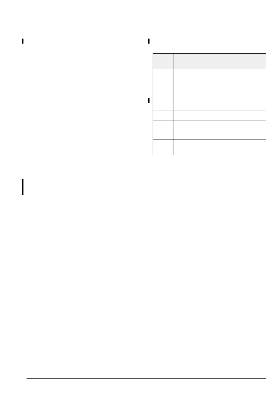
3.5. Version Number
Table 3≠5 shows where the MAS 3507D hardware ver-
sion, its software and additional information is located.
S
$3A
ACK
$69
ACK
S
$3B
Wait
ACK
d3, d2
ACK
d1, d0
Wait ACK
$0, $0
ACK
$0, d4
Wait
.... repeat for n data values
ACK
d3, d2
ACK
d1, d0
Wait ACK
d3, d2
ACK
d1, d0
Wait
Nak
P
S
$3A
ACK
$69
ACK
S
$3B
Wait
ACK
d3, d2
ACK
d1, d0
Wait
Nak
P
S
$3A
ACK
$6A
ACK
d3, d2
ACK
d1, d0
Wait ACK
P
Table 3≠5: MAS 3507D Version
Addr.
Content
Example Value
D1:$ff6
name of
MAS 3507D ver-
sion
0x03507
3507
D1:$ff7
hardware/software
design code
MAS 3507D F10
0x00601
(increases
for new
versions)
0601
D1:$ff9
description:
"MPEG 1/2.5 L23"
0x04d50
MP
D1:$ffa
0x04547
EG
D1:$ffb
0x02031
1
D1:$ffc
0x02f32
/2
D1:$ffd
0x02e35
.5
D1:$ffe
0x0204C
L
D1:$fff
0x03233
23

MAS 3507D
PRELIMINARY DATA SHEET
26
Micronas
3.6. Register Table
In Table 3≠6, the internal registers that are useful for
controlling the MAS 3507D are listed. They are acces-
sible by `register read/write' I
2
C commands (see Sec-
tion 3.3. on page 20).
Important note! Writing into undocumented registers
or read-only registers is always possible, but it is highly
recommended not to do so. It may damage the func-
tion of the firmware and may even lead to a complete
system crash of the decoder operation which can only
be restored by a reset.
3.6.1. DC/DC Converter
The DCCF Register controls both the internal voltage
monitor and DC/DC converter. Between output voltage
of the DC/DC converter and the internal voltage moni-
tor threshold an offset exists which is shown in the fol-
lowing table. Please pay attention to the fact, that I
2
C
protocol is working only if the processor is active
(WSEN = 1). However, the setting for the DCCF regis-
ter will remain active if the DCEN and WSEN lines are
deasserted
Table 3≠6: Command Register Table
Address
R/W
Name
Comment
Default
$8e
w
DCCF
Set DC/DC converter mode
(see Table 3≠7 on page 27)
$08000
$aa
r/w
Mute / Bypass
Tone Control
Forces a mute of the digital output
bypass Bass / Treble / Volume matrix
$0
$ed
1)
r
PIOData
Read back the PIO pin levels. The PI0 pin corresponds to bit
0 in the PIOData register.
This register can be used to detect the actual state of the
PIO pins, regardless of the PIO configuration.
$e6
r/w
StartupConfig
Shadows the start-up configuration set via PIO pins or I
2
C
command (valid are bits 8, 4...0 as described in Table 2≠8.
$e7
r/w
KPrescale
responsible for prescale of the tone filter (prevent overflows)
(see Section 3.6.3. on page 28)
$80000
$6b
r/w
KBass
responsible for increase / decrease of low frequencies
(see Section 3.6.3. on page 28)
$0
$6f
r/w
KTreble
responsible for increase / decrease of high frequencies
(see Section 3.6.3. on page 28)
$0
1) In order to get the right information of the PIO pin levels (except for PI19, Demand Pin), register $ed should be
read and evaluated. However, the Demand Pin PI19 is shadowed in bit 19 of register $c8.
PRELIMINARY DATA SHEET
MAS 3507D
Micronas
27
The DC/DC converter may generate interference noise
that could be unacceptable for some applications.
Thus the oscillator frequency may be adjusted in 16
steps in order to allow the system controller to select a
base frequency that does not interfere with an other
application.
The CLKI input provides the base clock f
CKLI
for the
frequency divider whose output is made symmetrical
with an additional divider by two. The divider quotient
is determined by the content of the DCCF register.
This register allows 32 settings generating a DC/DC
converter clock frequency f
dc
between:
(EQ 3)
Table 3≠7: DC/DC-converter switch frequency (Bits 8,
13..10 of DCCF-register)
DCCF Value
(hex)
1)
f
SW
Bit 8 = 0
Bit 8 = 1
0CC00
0C800
0C400
0C000
04C00
04800
04400
04000
01C00
01800
01400
01000
00C00
00800
00400
00000
156 kHz
160 kHz
163 kHz
167 kHz
171 kHz
175 kHz
179 kHz
184 kHz
188 kHz
194 kHz
199 kHz
204 kHz
210 kHz
216 kHz
223 kHz
230 kHz
238 kHz
245 kHz
253 kHz
263 kHz
272 kHz
283 kHz
295 kHz
307 kHz
320 kHz
335 kHz
351 kHz
368 kHz
387 kHz
409 kHz
433 kHz
460 kHz
1)
All other bits are set to zero (DC/DC-converter
output voltage = 3.0 V)
f
SW
f
CK LI
2
m
n
+
(
)
-------------------------
=
n
0 15
{ ,
}
m
16 32
,
{
}
,
Table 3≠8: DC Converter Output Voltages (Bits
16..14, Bit 9 of DCCF-register)
DCCF Value
(hex)
1)
DC/DC
Converter
Output
Internal
Voltage
Monitor
2)
1C000
18000
14000
10000
0C000
08000
04000
00000
1C200
18200
14200
10200
0C200
08200
04200
00200
3.5 V
3.4 V
3.3 V
3.2 V
3.1 V
3.0 V
2.9 V
2,8 V
2.7 V
2.6 V
2.5 V
2.4 V
2.3 V
2.2 V
2.1 V
2.0 V
3.3 V
3.2 V
3.1 V
3.0 V
2.9 V
2,8 V
2.7 V
2.6 V
2.5 V
2.4 V
2.3 V
2.2 V
2.1 V
2.0 V
1.9 V
1.8 V
1)
All other bits are set to zero (f
SW
= 230 kHz)
2)
PUP signal becomes inactive when output below

MAS 3507D
PRELIMINARY DATA SHEET
28
Micronas
3.6.2. Muting / Bypass Tone Control
To enable fast and simple mute functionality, set bit 0 in register $aa to `1'. Writing a `0' deactivates mute.
It is possible to bypass the complete bass / treble / volume control by setting bit 1 in register $aa (write a `2'). Reset-
ting bit 1 to `0' enables tone control again.
3.6.3. Bass and Treble Control
Tone control is implemented in the MAS 3507D. It
allows the control of bass and treble in a range up to
±15 dB, as Table 3≠9 shows. To prevent overflow or
clipping effects, the prescaler is built-in. The prescaler
decreases the overall gain of the tone filter, so the full
range up to +15 dB is usable without clipping.
To select a special setting, max. 3 coefficients have to
be written into registers of the MAS 3507D. This has to
be done via the `write register' I
2
C command (see
Section 3.3.3.).
Address
R/W
Name
Comment
Default
$aa
r/w
Mute / Bypass
Tone Control
0
1
2
Forces a mute of the digital output
no mute, Tone control active
mute output, but continue decoding
bypass Bass / Treble / Volume matrix
$0
Address
R/W
Name
Comment
Default
$e7
r/w
KPrescale
responsible for prescale of the tone filter (prevent overflows)
(see Section 2.4.3. on page 8)
$80000
$6b
r/w
KBass
responsible for increase / decrease of low frequencies
(see Section 2.4.3. on page 8)
$0
$6f
r/w
KTreble
responsible for increase / decrease of high frequencies
(see Section 2.4.3. on page 8)
$0

PRELIMINARY DATA SHEET
MAS 3507D
Micronas
29
Table 3≠9: Tone control registers
Boost in
dB
Bass
(Reg. $6b)
Treble
(Reg. $6f)
Prefactor
(Reg $e7)
+15
+14
+13
+12
+11
+10
+9
+8
+7
+6
+5
+4
+3
+2
+1
$61800
$5d400
$58800
$53800
$4e400
$48800
$42800
$3c000
$35800
$2e400
$27000
$1f800
$17c00
$10000
$800
$5f800
$58400
$51800
$49c00
$42c00
$3c000
$35400
$2ec00
$28400
$22000
$1c000
$16000
$10400
$ac00
$5400
$e9400
$e6800
$e3400
$dfc00
$dc000
$d7800
$d25c0
$cd000
$c6c00
$bfc00
$b8000
$af400
$a5800
$9a400
$8e000
0
0
0
$80000
-
1
-
2
-
3
-
4
-
5
-
6
-
7
-
8
-
9
-
10
-
11
-
12
-
13
-
14
-
15
$f7c00
$efc00
$e8000
$e0400
$d8c00
$d1800
$ca400
$c3c00
$bd400
$b7400
$b1800
$ac400
$a7400
$a2800
$9e400
$fac00
$f5c00
$f0c00
$ec000
$e7e00
$e2800
$de000
$d9800
$d5000
$d0400
$cbc00
$c6c00
$c1800
$bb400
$b2c00
$80000
$80000
$80000
$80000
$80000
$80000
$80000
$80000
$80000
$80000
$80000
$80000
$80000
$80000
$80000

MAS 3507D
PRELIMINARY DATA SHEET
30
Micronas
3.7. Memory Area
3.7.1. Status Memory
The memory cells given in the following table should be accessed by the `read control interface data' I
2
C command
(see Section 3.3.2. on page 21) because only the 16 LSBs of these memory blocks are used. The memory area
table is a consecutive memory block in the D0 memory that keeps all important status information that monitors the
MPEG decoding process. The `read control interface data' command resets the MPEG-FRAME-SYNC at PI4
as
described in Section 2.9.
3.7.1.1. MPEG Frame Counter
The counter will be incremented with each new frame that is decoded. With an invalid MPEG bit stream as its input
(e.g. if an invalid header is detected), the MAS 3507D resets the MPEGFrameCount cell to `0'. The MPEGFrame-
Count is also returned by the `default read' command as described in Section 3.3.9.
Table 3≠10: Status Memory Area
Address
Offset
1)
R/W
Name
Function
D0:$300
0
r
MPEGFrameCount
counts the MPEG frames
D0:$301
1
r
MPEGStatus1
MPEG header / status information
D0:$302
2
r
MPEGStatus2
MPEG header
D0:$303
3
r
CRCErrorCount
counts CRC errors during MPEG decoding
D0:$304
4
r
NumberOfAncillaryBits
number of bits in ancillary data
D0:$305
... $321
5
r
AncillaryData
organized in words a 16 bit (MSB first)
1) Offset applies to the `read control interface data' command
Address
Offset
R/W
Name
Function
D0:$300
0
r
MPEGFrameCount
counts the MPEG frames

PRELIMINARY DATA SHEET
MAS 3507D
Micronas
31
3.7.1.2. MPEG Status 1
The MPEG Status 1 contains the bits 15...11 of the MPEG header and some status bits. It will be set each frame,
directly after the header has been decoded from the bit stream.
Address
Offset
R/W
Name
Function
D0:$301
1
r
MPEGStatus 1
MPEG header / status information
Table 3≠11: MPEG Status 1
Bits
Name/Value
Comment
19, 15
%xxxx.x
don't care
14, 13
MPEG ID
%00
%01
%10
%11
Bits 11, 12 of the MPEG-header
MPEG 2.5
reserved
MPEG 2
MPEG 1
12, 11
Layer
%00
%01
%10
%11
Bits 13, 14 of the MPEG-header
reserved
Layer 3
Layer 2
Layer 1 (Not supported)
10
%1
not protected by CRC
9...2
private bits
1
%1
CRC Error
0
%1
invalid frame

MAS 3507D
PRELIMINARY DATA SHEET
32
Micronas
3.7.1.3. MPEG Status 2
The MPEG Status 2 contains the 16 LSBs of the MPEG header. It will be set directly after synchronizing to the bit
stream.
Address
Offset
R/W
Name
Function
D0:$302
2
r
MPEG Status 2
MPEG header
Table 3≠12: MPEG Status 2
Bits
Value/Name
Comment
19, 16
don't care
15...12
Bit rate index
MPEG 1
(Layer 2)
in kbit/s
MPEG 1
(Layer 3)
in kbit/s
MPEG 2 in kbit/s
(Layer 2 & 3)
MPEG 2.5 in kbit/s
%0000
%0001
%0010
%0011
%0100
%0101
%0110
%0111
%1000
%1001
%1010
%1011
%1100
%1101
%1110
%1111
free
32
48
56
64
80
96
112
128
160
192
224
256
320
384
forbidden
free
32
40
48
56
64
80
96
112
128
160
192
224
256
320
forbidden
free
8
16
24
32
40
48
56
64
80
96
112
128
144
160
forbidden
11, 10
Sampling frequency
MPEG 1
MPEG 2
MPEG 2.5
%00
%01
%10
%11
44.1 kHz
48 kHz
32 kHz
reserved
22.05 kHz
24 kHz
16 kHz
reserved
11.025 kHz
12 kHz
8 kHz
reserved
9
Padding bit
8
Private bit
7, 6
Mode
%00
%01
%10
%11
stereo
joint_stereo (intensity stereo / ms_stereo)
dual channel
single_channel
5, 4
Mode extension
(if joint stereo only)
intensity stereo
ms_stereo
%00
%01
%10
%11
off
on
off
on
off
off
on
on
3
%0 / 1
copyright not protected / copyright protected
PRELIMINARY DATA SHEET
MAS 3507D
Micronas
33
3.7.1.4. CRC Error Counter
The counter will be increased by each CRC error in the MPEG bit stream. It will not be reset by losing the synchroni-
zation.
3.7.1.5. Number Of Ancillary Bits
This cell displays the number of valid ancillary bits stored beginning at D0:$305.
2
%0 / 1
copy / original
1, 0
Emphasis
indicates the type of emphasis
%00
%01
%10
%11
none
50/15
µ
s
reserved
CCITT J.17
Table 3≠12: MPEG Status 2
Bits
Value/Name
Comment
Address
Offset
R/W
Name
Function
D0:$303
3
r
CRCErrorCount
counts CRC errors during MPEG decoding
Address
Offset
R/W
Name
Function
D0:$304
4
r
NumberOfAncillaryBits
number of bits in ancillary data

MAS 3507D
PRELIMINARY DATA SHEET
34
Micronas
3.7.1.6. Ancillary Data
This memory field contains the ancillary data. It is organized in words 16 bit each. The last ancillary bit transmitted in
a frame is placed at bit 0 in D0:$305. The position of the first ancillary data bit is locatable via the content of Number-
OfAncillaryBits.
An example: 17 bits ancillary data in a frame:
A possible `
read ancillary data
' algorithm would read the NumberOfAncillaryBits and the complete ancillary data
area using the telegram:
<$3a><$68><$31><$1e> (offset=4, n=30)
<$3a><$69><$3b><receive 30 16-bit words>
For reducing the I
2
C protocol transfer traffic, it may be useful to split up the `read ancillary data' algorithm into a first
part that reads NumberOfAncillaryBits and a second that reads only NumberOfAncillaryBits/16+1 words.
Address
Offset
R/W
Name
Function
D0:$305 ...
D0:$321
5
r
AncillaryData
organized in words a 16 bit (MSB first)
Table 3≠13: Ancillary data bit assignment
D0: $305
15 MSB
14
13
12
11
10
09
08
07
06
05
04
03
02
01
00 LSB
ancillary data
bit 1
bit 2
bit 3
bit 4
bit 5
bit 6
bit 7
bit 8
bit 9
bit 10
bit 11
bit 12
bit 13
bit 14
bit 15
bit 16
Table 3≠14: Ancillary data bit assignment
D0: $306
15 MSB
14
13
12
11
10
09
08
07
06
05
04
03
02
01
00 LSB
ancillary data
x
x
x
x
x
x
x
x
x
x
x
x
x
x
x
bit 0
PRELIMINARY DATA SHEET
MAS 3507D
Micronas
35
3.7.2. Configuration Memory
The configuration memory allows the controller advanced configuration possibilities, e.g. changing setups for the
crystal frequency or changing the digital format of the serial audio output data interface.
Table 3≠15: Configuration memory area
1)
1) Important note: Writing into undocumented memory cells is always possible, but it is highly recommended not to
do so. It may damage the function of the firmware and may even lead to a complete system crash of the decoder
operation which can only be restored by a reset.
Address
R/W
Name
Function
Default
D0:$36d
r/w
PLLOffset48
PLL offset (if f
s
= 48, 24, 12, 32, 16, or 8 kHz),
validate by `run $475' command
D0:$36e
r/w
PLLOffset44
PLL offset (if f
s
= 44.1, 22.05, 11.025 kHz),
validate by `run $475' command
D0:$36f
r/w
OutputConfig
Configuration of the I
2
S audio output interface
validate by `run $475' command
D1:$7f8
r/w
LL
Left
Left Gain
$80000
D1:$7f9
r/w
LR
Left
Right Gain
0
D1:$7fa
r/w
RL
Right
Left Gain
0
D1:$7fb
r/w
RR
Right
Right Gain
$80000

MAS 3507D
PRELIMINARY DATA SHEET
36
Micronas
3.7.2.1. PLL Offset for 44/48 kHz Sampling Frequency
With these memory cells it is possible to choose other
frequencies than the standard CLKI frequencies.
Please note:
≠ PLLOffset48 is valid for
f
s
= 48, 24, 12, 32, 16, or 8 kHz.
≠ PLLOffset44 is valid for
f
s
= 44.1, 22.05, 11.025 kHz.
Table 3≠16 shows the default values which will be set
by the firmware according to the start-up configuration.
It is also possible to run the MAS 3507D with other
clocks. In broadcast mode, it is necessary to adjust the
PLLOffsets to this clock, otherwise it will not lock to the
MPEG bit stream. In multimedia mode, it is recom-
mended to adjust the PLLOffsets to the crystal, other-
wise it would result in a frequency shift (music will be
played faster or slower). For adjusting, the following
procedure must be done:
≠ Calculate the PLLOffsets according to:
with
-
0.74 < PLLOffset < 0.74. This corresponds to
a frequency range of 14.31...14.73 MHz for the
crystal, if both 44.1 kHz and 48 kHz based sample
frequencies are used. The range is extended in an
application with a fixed sampling frequency, as
Table 3≠17 shows.
≠ Write the PLLOffsets to the memory (PLLOffset48
D0:$36d, PLLOffset44 D0:$36e).
≠ Send a `run $475' command. With the jump to this
address, the settings in the memory will be valid for
the internal processing.
Example:
A very common crystal frequency is 14.31818 MHz
(NTSC color subcarrier). The
and
are inside the range
-
0.74 ... 0.74.
Address
R/W
Name
Function
Default
D0:$36d
r/w
PLLOffset48
PLL offset (if f
s
= 48, 24, 12, 32, 16, or 8 kHz),
validate by `run $475' command
D0:$36e
r/w
PLLOffset44
PLL offset (if f
s
= 44.1, 22.05, 11.025 kHz),
validate by `run $475' command
Table 3≠16: PLLOffset48 and PLLOffset44
f
CLKI
PLLOffset48
PLLOffset44
14.725 MHz
0.351986
-
0.732862
f
CLKI
24,576 8
13
PLLOffset48
+
----------------------------------------------
22,5792 8
13
PLLOffset44
+
----------------------------------------------
=
=
Table 3≠17: f
ClkI
for max./ min. PLLOffsets
PLLOffset
f
CLKI
for f
s
related to
48 kHz
fCLKI for fs
related to
44.1 kHz
-
0.74
16.0365 MHz
14.7336 MHz
0.74
14.309 MHz
13.1465 MHz
PLLOffset48
24,576 8
14,31818
------------------------
13
≠
0,7314
=
=
PLLOffset44
22,5792 8
14,31818
---------------------------
13
≠
0,3843
≠
=
=

PRELIMINARY DATA SHEET
MAS 3507D
Micronas
37
3.7.2.2. Output Configuration
The content of this memory cell depends on the start-
up configuration and will be set by the firmware. Never-
theless, the audio output interface is configurable by
the software to work in different 16 bit/sample modes
and 32 bit/sample modes (see Section 2.7.4. on
page 13). For adjusting to this, the following procedure
has to be done:
≠ Choose the output mode (see Table 3≠18).
≠ Write this value to the memory (D0:$36f).
≠ Send a `run $475' command. With the jump to this
address, the settings in the memory will become
valid for the internal processing. This overrides all
start-up settings
3.7.3. Baseband Volume Matrix
The digital Baseband volume Matrix is used for con-
trolling the digital gain and a simple kind of stereo
basewidth enlargement as shown in Fig. 3≠2. Table 3≠
20 shows the proposed settings for the 4 volume
matrix coefficients for stereo, left and right mono. The
gain factors are given in fixed point notation. The gain
values may be written to the MAS 3507D by the con-
troller command 'write D1 memory'.
Address
R/W
Name
Function
Default
D0:$36f
r/w
OutputConfig
Configuration of the I
2
S audio output interface
validate by `run $475' command
Address
R/W
Name
Function
Default
D1:$7f8
r/w
LL
Left->Left gain
$80000
D1:$7f9
r/w
LR
Left->Right gain
$0
D1:$7fa
r/w
RL
Right->Left gain
$0
D1:$7fb
r/w
RR
Right->Right gain
$80000
Table 3≠18: Output Configuration
Bits
Value
Comment
19...15
%0000.0
don't care
14
%0
%1
SOC standard tim-
ing
SOC inverted tim-
ing
13..12
%00.
don't care
11
%0
%1
no delay
additional delay of
data related to word
strobe
10...6
%000.00
don't care
5
%0
%1
not invert
invert outgoing
word strobe signal
4
%0
%1
32 bits/sample
16 bits/sample
3...0
%0000
don't care
Table 3≠19: Bit Assignment of the Volume Cells
Bits
Name Value
Comment
19..0
LL/LR/RL/RR
-
524288/524288..524287/524288 =
-
1.0 .. 1.0
-
2^
-
19
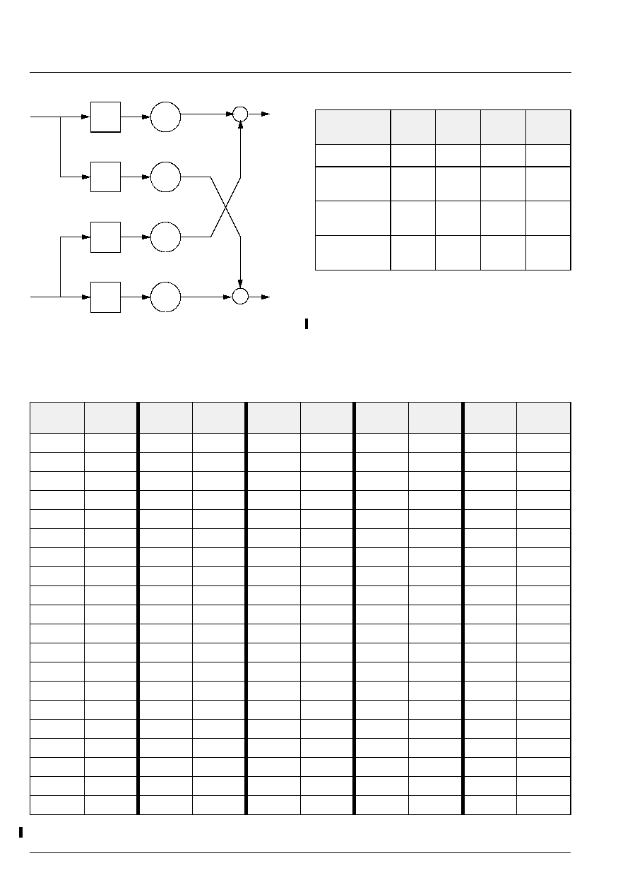
MAS 3507D
PRELIMINARY DATA SHEET
38
Micronas
Fig. 3≠2: Digital volume matrix
The fixed point gain values correspond to 20 bit 2's
complement notation. The conversion between fixed
point and 2's complement notation is done easily by
the algorithms described in Section 3.2.1.
Table 3≠21 contains the converted gain values as used in the 'write D1 memory' command
-
1
-
1
-
1
-
1
LL
LR
RL
RR
+
+
left audio
right audio
Table 3≠20: Settings for the digital volume matrix
Memory
location
D1:
$7f8
D1:
$7f9
D1:
$7fa
D1:
$7fb
Name
LL
LR
RL
RR
Stereo
(default)
-
1.0
0
0
-
1.0
Mono
left
-
1.0
-
1.0
0
0
Mono
right
0
0
-
1.0
-
1.0
Table 3≠21: Volume matrix conversion (dB into hexadecimal)
Volume
(in dB)
Hexa
decimal
Volume
(in dB)
Hexa
decimal
Volume
(in dB)
Hexa
decimal
Volume
(in dB)
Hexa
decimal
Volume
(in dB)
Hexa
decimal
0
80000
-
20
F3333
-
40
FEB85
-
60
FFDF4
-
80
FFFCC
-
1
8DEB8
-
21
F4979
-
41
FEDBF
-
61
FFE2D
-
81
FFFD1
-
2
9A537
-
22
F5D52
-
42
FEFBB
-
62
FFE60
-
82
FFFD6
-
3
A5621
-
23
F6F03
-
43
FF180
-
63
FFE8D
-
83
FFFDB
-
4
AF3CD
-
24
F7EC8
-
44
FF314
-
64
FFEB5
-
84
FFFDF
-
5
B8053
-
25
F8CD5
-
45
FF47C
-
65
FFED9
-
85
FFFE3
-
6
BFD92
-
26
F995B
-
46
FF5BC
-
66
FFEF9
-
86
FFFE6
-
7
C6D31
-
27
FA485
-
47
FF6DA
-
67
FFF16
-
87
FFFE9
-
8
CD0AD
-
28
FAE78
-
48
FF7D9
-
68
FFF2F
-
88
FFFEB
-
9
D2958
-
29
FB756
-
49
FF8BC
-
69
FFF46
-
89
FFFED
-
10
D785E
-
30
FBF3D
-
50
FF986
-
70
FFF5A
-
90
FFFEF
-
11
DBECC
-
31
FC648
-
51
FFA3A
-
71
FFF6C
-
91
FFFF1
-
12
DFD91
-
32
FCC8E
-
52
FFADB
-
72
FFF7C
-
92
FFFF3
-
13
E3583
-
33
FD227
-
53
FFB6A
-
73
FFF8B
-
93
FFFF4
-
14
E675F
-
34
FD723
-
54
FFBEA
-
74
FFF97
-
94
FFFF6
-
15
E93CF
-
35
FDB95
-
55
FFC5C
-
75
FFFA3
-
95
FFFF7
-
16
EBB6A
-
36
FDF8B
-
56
FFCC1
-
76
FFFAD
-
96
FFFF8
-
17
EDEB6
-
37
FE312
-
57
FFD1B
-
77
FFFB6
-
97
FFFF9
-
18
EFE2C
-
38
FE638
-
58
FFD6C
-
78
FFFBE
-
98
FFFF9
-
19
F1A36
-
39
FE905
-
59
FFDB4
-
79
FFFC5
-
99
FFFFA

PRELIMINARY DATA SHEET
MAS 3507D
Micronas
39
4. Specifications
4.1. Outline Dimensions
Fig. 4≠1:
44-Pin Plastic Leaded Chip Carrier Package
(PLCC44)
Weight approximately 2.5 g
Dimensions in mm
Fig. 4≠2:
44-Pin Plastic Quad Flat Package
(PMQFP44)
Weight approximately 0.4 g
Dimensions in mm
Note: Start pin and orientation of pin numbering is different for PLCC and PMQFP packages!
15.7
0.3
±
10 x 1.27 = 12.7
0.1
±
1.2 x 45
∞
1
40
39
29
28
18
17
7
6
1.6
0.1
5
8.6
5
2
2
x 45
∞
1.1
1.27
1.27
SPGS0027-2(P44/K)/1E
17.52
0.12
±
17.52
0.12
±
16.5
0.1
±
16.5
0.1
±
10 x 1.27 = 12.7
0.1
±
4.75
±
0.15
4.05
±
0.1
1.9
±
0.05
0.28
0.04
±
0.71
0.05
±
0.48
0.06
±
0.9
0.2
±
SPGS706000-2(P44)/1E
34
44
1
11
12
22
23
33
1.3
1.75
1.75
0.1
0.8
0.8
13.2
0.2
±
13.2
0.2
±
0.17
0.06
±
2.15
0.2
±
2.0
0.1
±
0.375
0.075
±
10
0.1
±
10
0.1
±
10 x 0.8 = 8
0.1
±
10 x 0.8 = 8
0.1
±
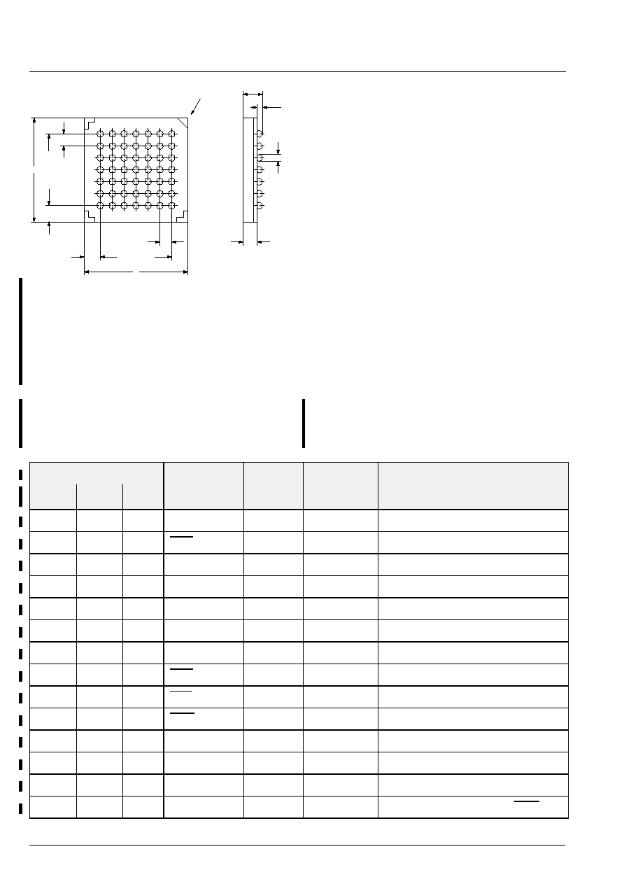
MAS 3507D
PRELIMINARY DATA SHEET
40
Micronas
Fig. 4≠3:
49-Ball Plastic Ball Grid Array
(PBGA49)
Weight approximately 0.13 g
Dimensions in mm
4.2. Pin Connections and Short Descriptions
NC
not connected, leave vacant
LV
If not used, leave vacant
X
obligatory, pin must be connected as described
in application information
VDD connect to positive supply
VSS connect to ground
0.46
6 x 0.8 = 4.8
SPGS0007-1/2E
7
0.8
7
6 x 0.8 = 4.8
0.8
A
B
C
D
E
F
G
1
2
3
4
5
6
7
1.4
0.36
1.04
1.1
1.1
A1 Ball Pad Corner
Pin No.
Pin Name
Type
Connection
Short Description
PMQFP
44-pin
PLCC
44-pin
PBGA
49-ball
Test Alias in ()
(If not used)
1
6
C3
TE
IN
VSS
Test Enable
2
5
C2
POR
IN
VDD
Reset, Active Low
3
4
B1
I2CC
IN/OUT
X
I
2
C Clock Line
4
3
D2
I2CD
IN/OUT
X
I
2
C Data Line
5
2
C1
VDD
SUPPLY
X
Positive Supply for Digital Parts
6
1
D1
VSS
SUPPLY
X
Ground Supply for Digital Parts
7
44
E2
DCEN
IN
VSS
Enable DC/DC Converter
8
43
E1
EOD
OUT
LV
PIO End of DMA, Active Low
9
42
F2
RTR
OUT
LV
PIO Ready to Read, Active Low
10
41
F1
RTW
OUT
LV
PIO Ready to Write, Active Low
11
40
G1
DCSG
SUPPLY
VSS
DC Converter Transistor Ground
12
39
E3
DCSO
OUT
VSS
DC Converter Transistor Open Drain
13
38
F3
VSENS
IN
VDD
DC Converter Voltage Sense
14
37
G2
PR
IN
X
PIO-DMA Request or Read/Write
PRELIMINARY DATA SHEET
MAS 3507D
Micronas
41
15
36
F4
PCS
IN
X
PIO Chip Select, Active Low
16
35
G3
PI19
IN/OUT
LV
PIO Data [19]
1. Demand Pin in SDI mode
2. data bit [7], MSB (PIO-DMA input
mode)
17
34
E4
PI18
IN/OUT
LV
PIO Data [18]
1. MPEG header bit 11
-
MPEG ID
(SDI mode)
2. data bit [6] (PIO-DMA input mode)
18
33
G4
PI17
IN/OUT
LV
PIO Data [17]
1. MPEG header bit 12 ≠ MPEG ID
(SDI mode)
2. data bit [5] (PIO-DMA input mode)
19
32
F5
PI16
IN/OUT
LV
PIO Data [16]
1. SIC*, alternative input for SIC (SDI
mode)
2. data bit [4] (PIO-DMA input mode)
20
31
G5
PI15
IN/OUT
LV
PIO Data [15]
1. SII*, alternative input for SII (SDI
mode)
2. data bit [3] (PIO-DMA input mode)
21
30
F6
PI14
IN/OUT
LV
PIO Data [14]
1. SID*, alternative input for SID (SDI
mode)
2. data bit [2] (PIO-DMA input mode)
22
29
G6
PI13
IN/OUT
LV
PIO Data [13]
1. MPEG header bit 13 ≠ Layer ID (SDI
mode)
2. data bit [1] (PIO-DMA input mode)
23
28
E5
PI12
IN/OUT
LV
PIO Data [12]
1. MPEG header bit 14 ≠ Layer ID (SDI
mode)
2. data bit [0] (PIO-DMA input mode)
24
27
E6
SOD
(PI11)
OUT
LV
Serial Output Data
25
26
F7
SOI
(PI10)
OUT
LV
Serial Output Frame Identification
26
25
D6
SOC
(PI9)
OUT
LV
Serial Output Clock
27
24
E7
PI8
IN
X
Start-up
1)
: Clock output scaler on / off
OUT
Operation
2)
: MPEG CRC error
28
23
D7
XVDD
SUPPLY
X
Positive Supply of Output Buffers
29
22
C6
XVSS
SUPPLY
X
Ground of Output Buffers
30
21
C7
SID
(PI7)
IN
X
Serial Input Data
31
20
B6
SII
(PI6)
IN
VSS
Serial Input Frame Identification
Pin No.
Pin Name
Type
Connection
Short Description
PMQFP
44-pin
PLCC
44-pin
PBGA
49-ball
Test Alias in ()
(If not used)
MAS 3507D
PRELIMINARY DATA SHEET
42
Micronas
32
19
B7
SIC
(PI5)
IN
X
Serial Input Clock
33
18
A7
PI4
IN
X
Start-up
1)
: Select SDI / PIO-DMA input
mode
OUT
Operation
2)
: MPEG-Frame Sync
34
17
B5
PI3
IN
X
Start-up
1)
:
Enable Layer 3 / Disable Layer 3
decoding
OUT
Operation
2)
: MPEG header bit 20
(Sampling frequency)
35
16
A6
PI2
IN
X
Start-up
1)
:
Enable Layer 2 / Disable Layer 2
decoding
OUT
Operation
2)
: MPEG header bit 21
(Sampling frequency)
36
15
B4
PI1
IN
X
Start-up
1)
:
SDO: Select 32-bit mode / 16-bit I
2
S
mode
OUT
Operation
2)
: MPEG header bit 30
(Emphasis)
37
14
A5
PI0
IN
X
Start-up
1)
:
Select Multimedia mode / Broadcast
mode
OUT
Operation
2)
: MPEG header bit 31
(Emphasis)
38
13
C4
CLKO
OUT
LV
Clock Output for the D/A converter
39
12
A4
PUP
OUT
LV
Power Up, i.e. status of voltage super-
vision
40
11
B3
WSEN
IN
X
Enable DSP and Start DC/DC Con-
verter
41
10
A3
WRDY
OUT
LV
If WSEN = 0: valid clock input at CLKI
If WSEN = 1: clock synthesizer PLL
locked
42
9
B2
AVDD
SUPPLY
VDD
Supply for analog circuits
43
8
A2
CLKI
IN
X
Clock input
44
7
A1
AVSS
SUPPLY
VSS
Ground supply for analog circuits
1)
Start-up configuration see Section 2.8.
2)
Not available in PIO-DMA mode, see Section 2.8.1.
Pin No.
Pin Name
Type
Connection
Short Description
PMQFP
44-pin
PLCC
44-pin
PBGA
49-ball
Test Alias in ()
(If not used)

PRELIMINARY DATA SHEET
MAS 3507D
Micronas
43
4.2.1. Pin Descriptions
4.2.1.1. Power Supply Pins
Connection of all power supply pins is mandatory for
the function of the MAS 3507D.
VDD
SUPPLY
VSS
SUPPLY
The VDD/VSS pair is internally connected with all digi-
tal modules of the MAS 3507D.
XVDD
SUPPLY
XVSS
SUPPLY
The XVDD/XVSS pins are internally connected with
the pin output buffers.
AVDD
SUPPLY
AVSS
SUPPLY
The AVDD/AVSS pair is connected internally with the
analog blocks of the MAS 3507D, i.e. clock synthesizer
and supply voltage supervision circuits.
4.2.1.2. DC/DC Converter Pins
DCEN
IN
The DCEN input signal enables the DC/DC converter
operation.
DCSG
SUPPLY
The DC converter Signal Ground pin is used as a
basepoint for the internal switching transistor of the
DC/DC converter. It must always be connected to
ground.
DCSO
OUT
DCSO is an open drain output and should be con-
nected with external circuitry (inductor/diode) to start
the DC/DC converter. When the DC/DC converter is
not used, it has to be connected to VSS.
VSENS
IN
The VSENS pin is the input for the DC/DC converter
feedback loop. It must be connected directly with the
Schottky diode and the capacitor as shown in Fig. 2≠3.
When the DC/DC converter is not used, it has to be
connected to VDD.
4.2.1.3. Control Lines
I2CC
SCL
IN/OUT
I2CD
SDA
IN/OUT
Standard I
2
C control lines. Normally there are Pullup-
resistors tied from each line to VDD.
4.2.1.4. Parallel Interface Lines
4.2.1.4.1. PIO Handshake Lines
PIO handshake lines are not used during start-up but
in operation mode. Read out of the status information
and the demand mode work in
µ
P-mode: set PCS = '0'
and PR = '1'. Usage of PIO-DMA mode is possible
with input mode via PIO.
PCS
IN
The PIO chip select must be set to `0' to activate the
PIO as Output in operation mode (e.g. PI19 = demand
signal in mutimedia mode & SDI input mode).
PR
IN
The PIO PR
must be set to `1' to validate data output
from MAS 3507D.
RTW
OUT
RTW is not supported by the built-in firmware.
RTR
OUT
RTR is only supported by the built-in firmware in PIO-
DMA input mode.
EOD
OUT
End of DMA (EOD) is only supported by the built-in
firmware in PIO-DMA input mode.
4.2.1.4.2. PIO Data Lines
The function of the parallel interface is separated into
two parts. During start-up, the PIO will read the start-
up configuration (independent from the PIO hand-
shake lines). This is done to define the environment for
the MAS 3507D (see Section 2.8.1. for details).
After start-up, the PIO will be switched to
µ
P-mode.
With the PR = `1' and the PCS = `0', the PIO interface
is defined as output and displays some status informa-
tion of the MPEG decoder. The PIO can be connected
to an external controller or to a display unit (e.g. LED).
The internal MPEG decoder firmware attaches specific
functions to the following pins:

MAS 3507D
PRELIMINARY DATA SHEET
44
Micronas
PI19
DEMAND PIN
OUT
When MAS 3507D is in multimedia mode it demands
with PI19 = '1' for new input data.
PI18
MPEG-IDEX
OUT
PI17
MPEG-ID
OUT
These pins mirror the according bits of the MPEG
header (see Table 2≠9 for details).
PI16
(SIC*)
IN
PI15
(SII*)
IN
PI14
(SID*
IN
The SIC*, SID*, and SII* may be configured as alterna-
tive serial input lines in order to support alternative
serial digital inputs.
PI13
LAYER ID
OUT
PI12
LAYER ID
OUT
These pins mirror the according bits of the MPEG
header (see Table 2≠9 for details).
PI8
MPEG-CRC-ERROR
OUT/IN
The MPEG-CRC-ERROR pin is activated if no suc-
cessful MPEG decoding is possible. The reason might
be that the CRC check of the MPEG Frame header
has detected an error or that no valid bit stream is
available. The error signal will stay active for the entire
duration of one MPEG frame.
During start-up, this pin is an input for enabling/dis-
abling the CLKO+divider (see Section 3.6.).
PI4
MPEG-FRAME-SYNC
OUT/IN
The MPEG-FRAME-SYNC signal indicates that a
MPEG header has been decoded properly and the
internal MPEG decoder is in a synched state. The
MPEG-FRAME-SYNC signal is inactive after Power
On Reset and will be activated if a valid MPEG Layer 2
or 3 header has been recognized. The signal will be
cleared if the ancillary data information is read out by
the controller via I
2
C interface.
During start-up, this pin sets either SDI- or PIO-DMA-
input mode (see Section 3.6.).
PI3
SAMPLING FREQUENCY
OUT
PI2
SAMPLING FREQUENCY
OUT
PI1
EMPHASIS
OUT
PI0
EMPHASIS
OUT
These pins mirror the according bits of the MPEG
header (see Table 2≠9 for details).
During start-up, these pins are input pins (see
Section 3.6.).
4.2.1.5. Voltage Supervision And Other Functions
CLKI
IN
This is the clock input of the MAS 3507D. CLKI should
be a buffered output of a crystal oscillator. Standard
clock frequency is 14.725. Others can be used, if
PLL_offset register is changed by I
2
C.
CLKO
OUT
The CLKO is an oversampling clock that is synchro-
nized to the digital audio data (SOD) and the frame
identification (SOI).
PUP
OUT
The PUP output indicates that the power supply volt-
age exceeds its minimal level (software adjustable).
WSEN
IN
WSEN enables DSP operation and starts DC/DC-con-
verter.
WRDY
OUT
WRDY has
two functions depending on the state of the
WSEN signal.
If WSEN = '0', it indicates that a valid clock has been
recognized at the CLKI clock input.
If WSEN = '1', the WRDY output will be set to `0' until
the internal clock synthesizer has locked to the incom-
ing audio data stream, and thus, the CLKO clock out-
put signal is valid.
4.2.1.6. Serial Input Interface
SID
IN
SII
IN
SIC
IN
Data, Frame Indication, and Clock line of the serial
input interface. The SII line should be connected with
VSS in the standard mode.
4.2.1.7. Serial Output Interface
SOD
OUT
SOI
OUT
SOC
OUT
Data, Frame Indication, and Clock line of the serial out-
put interface. The SOI indicates whether the left or the
right audio sample is transmitted. Besides the two
modes (selected by the PI1 during start-up), it is possi-
ble to reconfigure the interface.

PRELIMINARY DATA SHEET
MAS 3507D
Micronas
45
4.2.1.8. Miscellaneous
POR
IN
The Power On Reset pin is used to reset the digital
parts of the MAS 3507D. POR is a low active signal.
TE
IN
The TE pin is for production test only and must be con-
nected with VSS in all applications.
4.2.2. Pin Configurations
Fig. 4≠4: 44-pin PLCC package
Fig. 4≠5: 44-pin PMQFP package
7
8
9
10
11
12
13
14
15
16
17
39
38
37
36
35
34
33
32
31
30
29
18 19 20 21 22 23 24 25 26 27 28
6
5
4
3
2
1
44 43 42 41 40
AVSS
CLKI
AVDD
WRDY
WSEN
PUP
CLKO
PI0
PI1
PI2
PI3
DCSO
VSENS
PR
PCS
PI19
PI18
PI17
PI16
PI15
PI14
PI13
POR
I2CC
I2CD
VDD
VSS
TE
DCEN
EOD
RTR
RTW
DCSG
SIC
SII
SID
XVSS
XVDD
PI4
PI8
SOC
SOI
SOD
PI12
MAS 3507D
34
35
36
37
38
39
40
41
42
43
44
22
21
20
19
18
17
16
15
14
13
12
1
2
3
4
5
6
7
8
9
10 11
33 32 31 30 29 28 27 26 25 24 23
PI3
PI2
PI1
PI0
CLKO
PUP
WSEN
WRDY
AVDD
CLKI
AVSS
PI13
PI14
PI15
PI16
PI17
PI18
PI19
PCS
PR
VSENS
DCSO
SIC
SII
SID
XVSS
XVDD
PI4
PI8
SOC
SOI
SOD
PI12
POR
I2CC
I2CD
VDD
VSS
TE
DCEN
EOD
RTR
RTW
DCSG
MAS 3507D
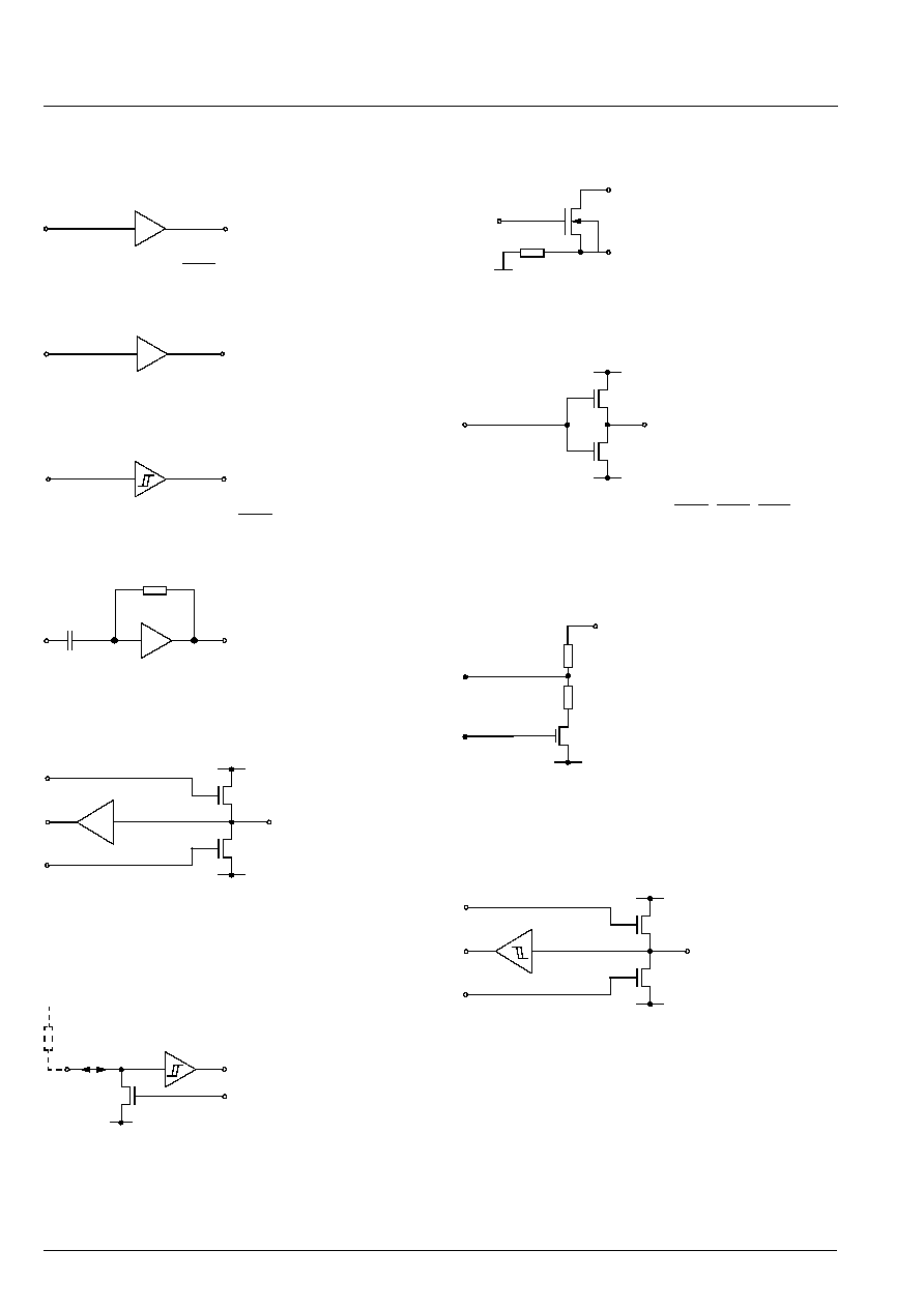
MAS 3507D
PRELIMINARY DATA SHEET
46
Micronas
4.2.3. Internal Pin Circuits
Fig. 4≠6: Input pins PCS, PR
Fig. 4≠7: Input pin TE, DCEN
Fig. 4≠8: Input pins WSEN, POR
Fig. 4≠9: Input pin CLKI
Fig. 4≠10: Input/Output pins PI0...PI4, PI8, SOC, SOI,
SOD, PI12..
.
PI19
Fig. 4≠11: Input/Output pins I2CC, I2CD
Fig. 4≠12: Input/Output pins DCSO, DCSG
Fig. 4≠13: Output pins WRDY, RTW, EOD
,
RTR
,
CLKO, PUP
Fig. 4≠14: Input pin VSENS
Fig. 4≠15: Input/Output pins SIC, SII, SID
TTLIN
VDD
P
N
VSS
VDD
N
VSS
DCSO
DCSG
VSS
VDD
VSS
N
P
VSS
VSENS
VDD
P
N
VSS

PRELIMINARY DATA SHEET
MAS 3507D
Micronas
47
4.2.4. Electrical Characteristics
4.2.4.1. Absolute Maximum Ratings
Stresses beyond those listed in the "Absolute Maximum Ratings" may cause permanent damage to the device. This
is a stress rating only. Functional operation of the device at these or any other conditions beyond those indicated in
the "Recommended Operating Conditions/Characteristics" of this specification is not implied. Exposure to absolute
maximum ratings conditions for extended periods may affect device reliability.
4.2.4.2. Recommended Operating Conditions
Symbol
Parameter
Pin
Name
Min.
Max.
Unit
T
A
Ambient Operating Temperature
-
30
85
∞C
T
S
Storage Temperature
-
40
125
∞C
P
MAX
Power dissipation
VDD,
XVDD,
AVDD
600
400 (PBGA)
mW
V
SUP
Supply voltage
VDD,
XVDD,
AVDD
5.5
V
V
Idig
Input voltage, all digital inputs
-
0.3
V
SUP
+0.3
V
I
Idig
Input current, all digital inputs
-
20
+20
mA
I
Out
Current, all digital output
0.5
A
I
OutDC
Current
DCSO
1.5
A
Symbol
Parameter
Pin
Name
Min.
Typ.
Max.
Unit
T
A
Ambient temperature range
-
30
85
∞C
V
SUP
Supply voltage
VDD,
XVDD,
AVDD
2.5
2.7
3.6
V
Reference Frequency Generation
CLK
F
Clock Frequency
1)
CLKI
14.725
MHz
CLK
I_V
Clock Input Voltage
0
V
SUP
V
CLK
Amp
Clock Amplitude
0.5
V
pp
1)
range acc. to Section 3.7.2.1.
MAS 3507D
PRELIMINARY DATA SHEET
48
Micronas
Levels
I
IL27
Input Low Voltage
@V
SUP
= 2.5 V ... 3.6 V
POR
I2CC,
I2CD,
DCEN,
WSEN
0.4
V
I
IH36
Input High Voltage
@V
SUP
= 2.5 V ... 3.6 V
1.8
V
I
IH33
Input High Voltage
@V
SUP
= 2.5 V ... 3.3 V
1.7
V
I
IH30
Input High Voltage
@V
SUP
= 2.5 V ... 3.0 V
1.6
V
I
ILD
Input Low Voltage
PI<i>
2)
,
SII,
SIC,
SID,
PR,
PCS,
TE,
0.4
V
I
IHD
Input High Voltage
V
SUP
-
0.5
V
T
rf
Rise / Fall time of digital inputs
PI<i>,
SII,
SIC,
SID,
PR,
PCS,
CLKI
10
ns
D
cycle
Duty cycle of digital clock inputs
SIC, CLKI
40
50
60
%
DC-DC converter external circuitry
C
1
Blocking Capacitor
(25 m
ESR)
3)
VSENS,
DCSG
330
µ
F
V
F
Schottky Diode Forward voltage
4)
DCSO,
VSENS
0.35
0.45
V
L
Inductance of Ferrite ring core coil
5)
(50 m
),VAC 616/103
DCSO
20
µ
H
2)
i = 0 to 4, 8 , 12 to 19
3)
Sanyo Oscon 6SA330M
(distributed by Endrich Bauelemente, D-72202 Nagold-lselshausen, www.endrich.com)
4)
ZETEX ZMCS1000
(distributed by ZETEX, D-81673 M¸nchen,
europe.sales@zetex.com
)
, standard Schottky 1N5817
5)
C8 R/4L, SDS0604 (distributed by Endrich Bauelemente, see above)
Symbol
Parameter
Pin
Name
Min.
Typ.
Max.
Unit
PRELIMINARY DATA SHEET
MAS 3507D
Micronas
49
4.2.4.3. Characteristics
at T
A
=
-
30 to 85 ∞C, V
SUP
= 2.5 to 3.6 V, typ. values at T
A
= 27∞C, V
SUP
= 2.7 V, CLK
F
= 14.725 MHz, duty
cycle = 50%
Symbol
Parameter
Pin
Name
Min.
Typ.
Max.
Unit
Test Conditions
Supply Voltage
I
SUP
Current consumption
VDD,
XVDD,
AVDD
32
mA
2.7 V, sampling
frequency
32kHz
17
mA
2.7 V, sampling
frequency
24 kHz
11
mA
2.7 V, sampling
frequency
12 kHz
Digital Outputs and Inputs
V
DOL
Output Low Voltage
SOI
1)
,
SOC
1)
,
SOD
1)
,
EOD,
RTR,
RTW,
WRDY,
PUP,
CLKO
PI<i>
0.3
V
I
load
= 6mA
V
DIH
Output High Voltage
V
SUP
-
0.3
V
I
load
= 6mA
Z
DigI
Input Impedance
PI<i>,
SII,
SIC,
SID,
PR,
PCS,
CLKI
7
pF
I
DLeak
Digital Input Leakage
Current
-
1
1
µ
A
0 V < V
pin
< V
SUP
1)
in low inpedance mode
MAS 3507D
PRELIMINARY DATA SHEET
50
Micronas
4.2.4.3.1. I
2
C Characteristics
at T
A
=
-
30 to 85 ∞C, V
SUP
=2.5 to 3.6 V, typ. values at T
A
= 27∞C, V
SUP
= 2.7 V, CLK
F
= 14.725 MHz, duty
cycle = 50 %
Fig. 4≠16: I
2
C timing diagram
Symbol
Parameter
Pin
Name
Min.
Typ.
Max.
Unit
Test Conditions
R
ON
Output resistance
I2CC,
I2CD
60
I
load
= 5 mA,
V
SUP
= 2.7 V
f
I2C
I
2
C Bus Frequency
I2CC
400
kHz
t
I2C1
I
2
C START Condition Setup
Time
I2CC,
I2CD
300
ns
t
I2C2
I
2
C STOP Condition Setup
Time
I2CC,
I2CD
300
ns
t
I2C3
I
2
C Clock Low Pulse Time
I2CC
1250
ns
t
I2C4
I
2
C Clock High Pulse Time
I2CC
1250
ns
t
I2C5
I
2
C Data Hold Time before
rising edge of clock
I2CC
80
ns
t
I2C6
I
2
C Data Hold Time after
falling edge of clock
I2CC
80
ns
V
I2COL
I
2
C Output Low Voltage
I2CC,
I2CD
0.3
V
I
LOAD
= 5 mA
I
I2COH
I
2
C Output high leakage
current
I2CC,
I2CD
1
uA
V
I2CH
= 3.6 V
t
I2COL1
I
2
C Data Output Hold Time
after falling edge of clock
I2CC,
I2CD
20
ns
t
I2COL2
I
2
C Data Output Setup Time
before rising edge of clock
I2CC,
I2CD
250
ns
f
I2C
= 400kHz
I2CC
I2CD as input
I2CD as output
t
I2C1
t
I2C5
t
I2C6
t
I2C2
t
I2C4
t
I2C3
1/f
I2C
t
I2COL2
t
IC2OL1
H
L
H
L
H
L

PRELIMINARY DATA SHEET
MAS 3507D
Micronas
51
4.2.4.3.2. I
2
S Bus Characteristics ≠ SDI
at T
A
=
-
30 to 85 ∞C, V
SUP
=2.5 to 3.6 V, typ. values at T
A
= 27∞C, V
SUP
= 2.7 V, CLK
F
= 14.725 MHz, duty
cycle = 50 %
Fig. 4≠17: Serial input
Symbol
Parameter
Pin
Name
Min.
Typ.
Max.
Unit
Test Conditions
t
SICLK
I
2
S Clock Input Clockperiod
SIC
960
ns
multimedia mode, mean
data rate < 150 kbit/s
t
SIIDS
I
2
S Data SetupTime before
falling edge of clock
SIC,
SID
50
t
SICLK
-
100
ns
t
SIIDH
I
2
S data hold time
SID
50
ns
t
bw
Burst wait time
SIC,
SID
480
H
L
H
L
H
L
SIC
(SII)
SID
T
SICLK
T
SIIDH
T
SIIDS
MAS 3507D
PRELIMINARY DATA SHEET
52
Micronas
4.2.4.3.3. I
2
S Characteristics ≠ SDO
at T
A
=
-
30 to 85 ∞C, V
SUP
= 2.5 to 3.6 V, typ. values at T
A
= 27∞C, V
SUP
= 2.7 V, CLK
F
= 14.725 MHz, duty
cycle = 50 %
Fig. 4≠18: Serial output
Symbol
Parameter
Pin
Name
Min.
Typ.
Max.
Unit
Test Conditions
t
SOCLK
I
2
S Clock Output Period
SOC
325
ns
48 kHz Stereo
32 bit/sample
t
SOISS
I
2
S Wordstrobe Hold Time
after falling edge of clock
SOC,
SOI
10
t
SOCLK
/
2
ns
t
SOODC
I
2
S Data Hold Time after
falling edge of clock
SOC,
SOD
10
t
SOCLK
/
2
ns
H
L
H
L
H
L
SOC
SOI
SOD
T
SOCLK
T
SOISS
T
SOISS
T
SOODC
PRELIMINARY DATA SHEET
MAS 3507D
Micronas
53
4.2.4.4. Firmware Characteristics
at T
A
=
-
30 to 85 ∞C, V
SUP
= 2.5 to 3.6 V, typ. values at T
A
= 27∞C, V
SUP
= 2.7 V, CLK
F
= 14.725 MHz, duty
cycle = 50 %
4.2.4.4.1. Input Timing Parameters of the MultimediaMode
Fig. 4≠19: Demand mode
T
sdstart
refers to the maximal response time for a serial data source to start data transmission with respect to the ris-
ing edge of the demand signal at the pin PI19.
T
sdstop
refers to the maximal response time for a serial data source to stop data transmission with respect to the fall-
ing edge of the demand signal at the pin PI19.
Symbol
Parameter
Min.
Typ.
Max.
Unit
Test Conditions
Synchronization Times
t
mpgsync
Synchronization on MPEG Bit Streams
12...36
72
ms
f
s
= 32 kHz, MPEG 2.5
Ranges
PLLRange
Tracking range of sampling clock
recovery PLL
-
200
200
ppm
Broadcast mode
Symbol
Parameter
Pin Name
Min.
Typ.
Max.
Unit
Test Conditions
T
sdstart
Reaction time for data source
PI19
3.1
5.7
ms
f
s
= 48 kHz,
320...64 kbit/s
T
sdstart
Reaction time for data source
4.2
9.2
ms
f
s
= 24 kHz,
320...32 kbit/s
T
sdstar
Reaction time for data source
23.1
25.6
ms
f
s
= 12 kHz,
64...16 kbit/s
T
sdstar
Reaction time for data source
34.8
38.4
ms
f
s
= 8 kHz,
64...8 kbit/s
T
sdstop
Reaction time for data source
1.3
ms
H
L
T
sdstart
T
sdstop
PI19
MAS 3507D
PRELIMINARY DATA SHEET
54
Micronas
4.2.4.5. DC/DC Converter Characteristics
at T
A
=
-
30 to 85 ∞C, V
SUP
= 3.0 V, CLK
F
= 14.725 MHz, f
sw
= 230 kHz, typ. values at T
A
= +27 ∞C
All measurements are made with a C8 R/4L 20
µ
H, 25 m
ferrite ring-core coil, Zetex ZLMCS1000 Schottky diode,
and Sanyo/Oscon 6SA330M 330
µ
F, 25 m
ESR capacitors at input and output (see Section 4.2.4. on page 47).
Symbol
Parameter
Pin Name
Min.
Typ.
Max.
Unit
Test Conditions
V
IN1
Minimum Start-Up Input
Voltage
0.9
1.0
V
I
LOAD
= 0 mA
DCCF = $08000
(Reset)
V
IN2
Minimum Operating Voltage
0.6
0.8
V
I
LOAD
= 55 mA,
DCCF = $08000
(Reset)
1.3
1.8
V
I
LOAD
= 250 mA,
DCCF = $08000
(Reset)
V
OUT
Output Voltage
2.0
1)
3.5
V
see Section 4.2.4.6.
dV
OUT
/dV
IN
/
V
OUT
Line Regulation
1
%
V
IN
= 1.0...3.0 V,
I
LOAD
= 55 mA
dV
OUT
/dI
LOAD
/
V
OUT
Load Regulation
0.6
%
V
IN
= 1.2 V,
I
LOAD
= 0...55 mA,
f
SW
= 230 kHz
dV
OUT
/dI
LOAD
/
V
OUT
Load Regulation
1.2
%
V
IN
= 1.2 V,
I
LOAD
= 0...55 mA,
f
SW
= 165 kHz
h
max
Maximum Efficiency
90
%
I
SUPPLY
Supply Current
1.1
5
mA
V
IN
= 3.0 V, I
LOAD
= 0,
includ. switch current
I
L,MAX
Inductor Current Limit
DCSO,
DCSG
1.0
1.4
A
R
ON
Switch On-Resistance
DCSO,
DCSG
0.2
0.4
T
j
= 25
∞
C
I
LEAK
Switch Leakage Current
DCSO,
DCSG
0.1
1
µ
A
T
j
= 25
∞
C
f
SW
Switch Frequency
DCSO,
DCSG
156
230
460
kHz
Depending on DCCF
t
START
Start Up Time to PUP-Enable
DCEN
,
PUP
8
ms
V
IN
= 1.0 V,
I
LOAD
= 1 mA,
PUPLIM = 010 (Reset)
V
STARTTRAN
Start-Up to Normal Mode
Transition Voltage
VSENSE
1.9
V
1) see Section 4.2.4.2.
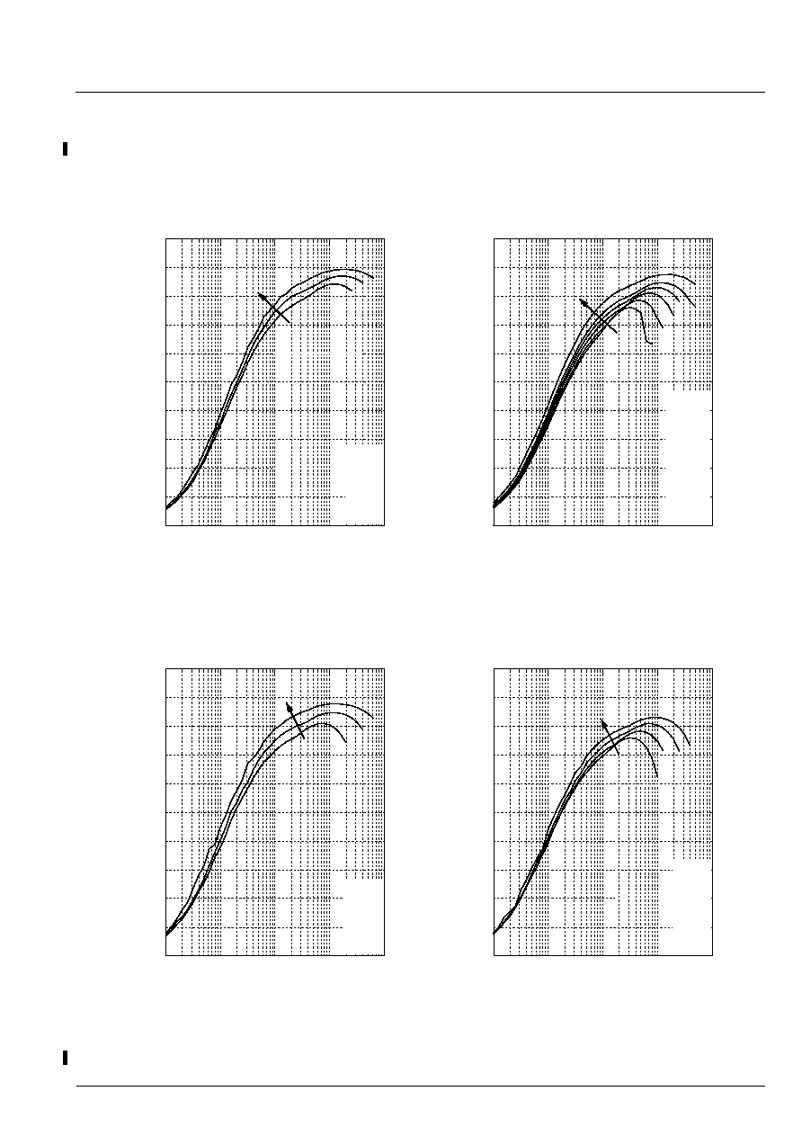
PRELIMINARY DATA SHEET
MAS 3507D
Micronas
55
4.2.4.6. Typical Performance Characteristics
Fig. 4≠20: Efficiency vs. Load Current
Load Current (A)
0
20
40
60
80
100
Efficiency (%)
Efficiency vs. Load Current
(Vout=2.7V)
Load Current (A)
0
20
40
60
80
100
Efficiency (%)
Efficiency vs. Load Current
(Vout=3.5V)
Load Current (A)
0
20
40
60
80
100
Efficiency (%)
Efficiency vs. Load Current
(Vout=2.2V)
Load Current (A)
0
20
40
60
80
100
Efficiency (%)
Efficiency vs. Load Current
(Vout=3.0V)
10
10
10
10
1
-4
-3
-2
-1
10
10
10
10
1
-4
-3
-2
-1
10
10
10
10
1
-4
-3
-2
-1
10
10
10
10
1
-4
-3
-2
-1
Vin:
2.4V
1.8V
1.5V
1.2V
0.9V
0.7V
Vin:
3.0V
2.4V
1.8V
Vin:
2.4V
1.8V
1.2V
Vin:
1.5V
1.2V
0.9V
0.7V
3.0 V
1.8 V
Vin
0.7 V
2.4 V
Vin
0.7 V
1.5 V
Vin
2.4 V
1.2 V
Vin
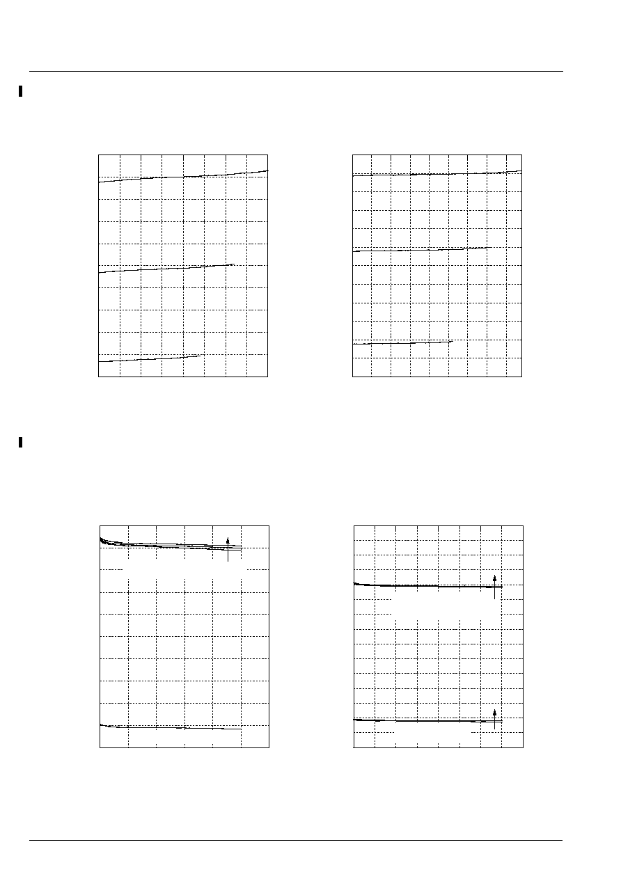
MAS 3507D
PRELIMINARY DATA SHEET
56
Micronas
Fig. 4≠21: Output Voltage vs. Input Voltage
Fig. 4≠22: Output Voltage vs. Load Current
1.5
2
2.5
3
3.5
Input Voltage (V)
2.6
2.8
3
3.2
3.4
3.6
Output Voltage (V)
Output Voltage vs. Input Voltage
Iload=250mA
0.9
1.4
1.9
2.4
2.9
Input Voltage (V)
2
2.2
2.4
2.6
2.8
3
3.2
Output Voltage (V)
Output Voltage vs. Input Voltage
Iload=50mA
3.5 V
3.1 V
2.7 V
3.1 V
2.2 V
2.7 V
0
0.1
0.2
0.3
Load Current (A)
2.6
2.8
3
3.2
3.4
3.6
Output Voltage (V)
Output Voltage
vs. Load Current
0
0.02
0.04
0.06
0.08
Load Current (A)
2
2.2
2.4
2.6
2.8
3
3.2
3.4
Output Voltage
Output Voltage
vs. Load Current
Vin=3V, 2.4V, 1.8V
Vin=2.4V
Vin=1.5V, 0.9V
Vin=1.5V, 0.9V
Vin
Vin
Vin
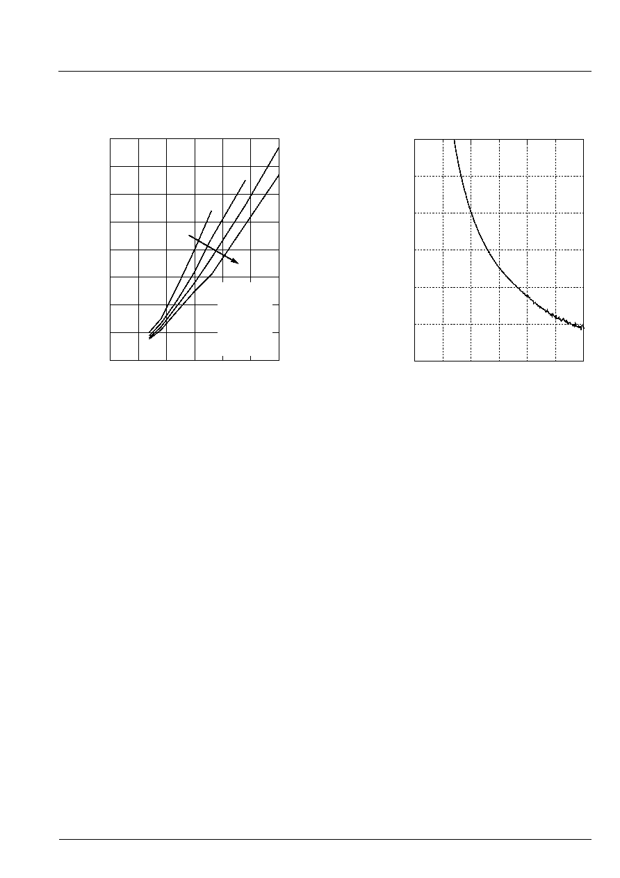
PRELIMINARY DATA SHEET
MAS 3507D
Micronas
57
Fig. 4≠23: Maximum Load Current vs. Input Voltage
Fig. 4≠24: No Load Supply Current vs. Input Voltage
0 1
2
3
Input Voltage (V)
0
0.2
0.4
0.6
0.8
Maximum Load Current (A)
Maximum Load Current
vs. Input Voltage
Vout=
3.5V
3.1V
2.7V
2.2V
3.5V
2.2V
V
out
0 1
2
3
Input Voltage (V)
0
2.0
4.0
6.0
No Load Supply Current (mA)
No Load Supply Current
vs. Input Voltage
V
out
= 3 V

MAS 3507D
PRELIMINARY DATA SHEET
58
Micronas
Fig. 4≠25: Load Transient-Response
Fig. 4≠26: Line Transient-Response
Fig. 4≠27: Startup Waveform
500.00
µ
s/Div
V
in
= 1.2 V; V
out
= 3 V
1 Load Current
200.0 mA/Div
2 Output Voltage
100.0 mV/Div / AC-coupled
3 Inductor Current
500.0 mA/Div
3 V
0 A
0 A
I
load
= 100 mA; V
out
= 3 V
1 V
in
2.000 V/Div
2 Output Voltage
50.00 mV/Div / AC-coupled
3 Inductor Current 200.0 mA/Div
5.00 ms/Div
3 V
2 V
20
0
m
A
V
in
= 1 V; I
load
= 0 mA
1 V (DCEN)
2.000 V/Div
2 V (PUP)
2.000 V/Div
3 Inductor Current
500.0 mA/Div
4 Output Voltage
2.000 V/Div
500
µ
s/Div
0 A
3 V
3 V
3 V

PRELIMINARY DATA SHEET
MAS 3507D
Micronas
59

All information and data contained in this data sheet are without any
commitment, are not to be considered as an offer for conclusion of a
contract, nor shall they be construed as to create any liability. Any new
issue of this data sheet invalidates previous issues. Product availability
and delivery are exclusively subject to our respective order confirmation
form; the same applies to orders based on development samples deliv-
ered. By this publication, Micronas GmbH does not assume responsibil-
ity for patent infringements or other rights of third parties which may
result from its use.
Further, Micronas GmbH reserves the right to revise this publication and
to make changes to its content, at any time, without obligation to notify
any person or entity of such revisions or changes.
No part of this publication may be reproduced, photocopied, stored on a
retrieval system, or transmitted without the express written consent of
Micronas GmbH.
MAS 3507D
PRELIMINARY DATA SHEET
60
Micronas
Micronas GmbH
Hans-Bunte-Strasse 19
D-79108 Freiburg (Germany)
P.O. Box 840
D-79008 Freiburg (Germany)
Tel. +49-761-517-0
Fax +49-761-517-2174
E-mail: docservice@micronas.com
Internet: www.micronas.com
Printed in Germany
Order No. 6251-459-3PD
5. Data Sheet History
1. Preliminary data sheet: "MAS 3507D MPEG 1/2
Layer2/3 Audio Decoder", Feb. 25, 1998,
6251-459-1PD. First release of the preliminary data
sheet.
2. Preliminary data sheet: "MAS 3507D MPEG 1/2
Layer 2/3 Audio Decoder", Oct. 21, 1998,
6251-459-2PD. Second release of the preliminary data
sheet. Major changes:
≠ Table 3≠20: Volume matrix conversion added
≠ Address for Prefactor register corrected
≠ Definition for register $aa changed
≠ Fig. 4≠1: Outline Dimension for PLCC44 changed
≠ Fig. 4≠2: PQFP44 package diagram changed
≠ Fig. 4≠3 and Fig. 4≠4: Pin configurations added
3. Preliminary data sheet: "MAS 3507D MPEG 1/2
Layer 2/3 Audio Decoder, March 16, 2000,
6251-459-3PD. Third release of the preliminary data
sheet.