 | –≠–ª–µ–∫—Ç—Ä–æ–Ω–Ω—ã–π –∫–æ–º–ø–æ–Ω–µ–Ω—Ç: MSP3400D | –°–∫–∞—á–∞—Ç—å:  PDF PDF  ZIP ZIP |

MSP 3400D,
MSP 3410D
Multistandard
Sound Processors
Edition May 14, 1999
6251-482-2PD
PRELIMINARY DATA SHEET
MICRONAS
MICRONAS

MSP 34x0D
PRELIMINARY DATA SHEET
2
Micronas
Contents
Page
Section
Title
5
1.
Introduction
5
1.1.
Common Features of MSP 34x0D
5
1.2.
Specific Features of MSP 3410D
6
2.
Basic Features of the MSP 34x0D
6
2.1.
Demodulator and NICAM Decoder Section
6
2.2.
DSP Section (Audio Baseband Processing)
6
2.3.
Analog Section
7
3.
Application Fields of the MSP 34x0D
7
3.1.
NICAM plus FM/AM-Mono
7
3.2.
German 2-Carrier System (Dual-FM System)
10
4.
Architecture of the MSP 34x0D
10
4.1.
Demodulator and NICAM Decoder Section
10
4.1.1.
Analog Sound IF ≠ Input Section
11
4.1.2.
Quadrature Mixers
11
4.1.3.
Low-pass Filtering Block for Mixed Sound IF Signals
12
4.1.4.
Phase and AM Discrimination
12
4.1.5.
Differentiators
12
4.1.6.
Low-pass Filter Block for Demodulated Signals
12
4.1.7.
High-Deviation FM Mode
12
4.1.8.
FM Carrier Mute Function in the Dual-Carrier FM Mode
12
4.1.9.
DQPSK Decoder
12
4.1.10.
NICAM Decoder
13
4.2.
Analog Section
13
4.2.1.
SCART Switching Facilities
13
4.2.2.
Stand-by Mode
13
4.3.
DSP Section (Audio Baseband Processing)
13
4.3.1.
Dual-Carrier FM Stereo/Bilingual Detection
15
4.4.
Audio PLL and Crystal Specifications
15
4.5.
ADR Bus Interface
15
4.6.
Digital Control Output Pins
16
4.7.
I
2
S Bus Interface
17
5.
I
2
C Bus Interface: Device and Subaddresses
18
5.1.
Protocol Description
19
5.2.
Proposal for MSP 34x0D I
2
C Telegrams
19
5.2.1.
Symbols
19
5.2.2.
Write Telegrams
19
5.2.3.
Read Telegrams
19
5.2.4.
Examples
20
5.3.
Start-Up Sequence: Power-Up and I
2
C-Controlling

Contents, continued
Page
Section
Title
PRELIMINARY DATA SHEET
MSP 34x0D
Micronas
3
21
6.
Programming the Demodulator and NICAM Decoder Section
21
6.1.
Short-Programming and General Programming of the Demodulator Part
22
6.2.
Demodulator Write Registers: Table and Addresses
22
6.3.
Demodulator Read Registers: Table and Addresses
23
6.4.
Demodulator Write Registers for Short-Programming: Functions and Values
23
6.4.1.
Demodulator Short-Programming
24
6.4.2.
AUTO_FM/AM: Automatic Switching between NICAM and FM/AM-Mono
25
6.5.
Demodulator Write Registers for the General Programming Mode: Functions and Values
25
6.5.1.
Register `AD_CV'
27
6.5.2.
Register `MODE_REG'
28
6.5.3.
FIR Parameter
30
6.5.4.
DCO Registers
31
6.6.
Demodulator Read Registers: Functions and Values
32
6.6.1.
Autodetection of Terrestrial TV Audio Standards
32
6.6.2.
C_AD_BITS
32
6.6.3.
ADD_BITS [10...3] 0038
hex
32
6.6.4.
CIB_BITS
33
6.6.5.
ERROR_RATE 0057
hex
33
6.6.6.
CONC_CT (for compatibility with MSP 3410B)
33
6.6.7.
FAWCT_IST (for compatibility with MSP 3410B)
33
6.6.8.
PLL_CAPS
33
6.6.9.
AGC_GAIN
33
6.7.
Sequences to Transmit Parameters and to Start Processing
35
6.8.
Software Proposals for Multistandard TV Sets
35
6.8.1.
Multistandard Including System B/G with NICAM/FM-Mono only
35
6.8.2.
Multistandard Including System I with NICAM/FM-Mono only
35
6.8.3.
Multistandard Including System B/G with NICAM/FM-Mono and German DUAL-FM
35
6.8.4.
Satellite Mode
35
6.8.5.
Automatic Search Function for FM Carrier Detection
37
7.
Programming the DSP Section (Audio Baseband Processing)
37
7.1.
DSP Write Registers: Table and Addresses
39
7.2.
DSP Read Registers: Table and Addresses
40
7.3.
DSP Write Registers: Functions and Values
40
7.3.1.
Volume ≠ Loudspeaker and Headphone Channel
41
7.3.2.
Balance ≠ Loudspeaker and Headphone Channel
41
7.3.3.
Bass ≠ Loudspeaker and Headphone Channel
42
7.3.4.
Treble ≠ Loudspeaker and Headphone Channel
42
7.3.5.
Loudness ≠ Loudspeaker and Headphone Channel
43
7.3.6.
Spatial Effects ≠ Loudspeaker Channel
44
7.3.7.
Volume ≠ SCART1 and SCART2 Channel
44
7.3.8.
Channel Source Modes
45
7.3.9.
Channel Matrix Modes
45
7.3.10.
SCART Prescale
46
7.3.11.
FM/AM Prescale
46
7.3.12.
FM Matrix Modes (see also Table 4≠1)
46
7.3.13.
FM Fixed Deemphasis

MSP 34x0D
PRELIMINARY DATA SHEET
4
Micronas
Contents, continued
Page
Section
Title
46
7.3.14.
FM Adaptive Deemphasis
47
7.3.15.
NICAM Prescale
47
7.3.16.
NICAM Deemphasis
47
7.3.17.
I
2
S1 and I
2
S2 Prescale
47
7.3.18.
ACB Register
48
7.3.19.
Beeper
48
7.3.20.
Identification Mode
48
7.3.21.
FM DC Notch
48
7.3.22.
Mode Tone Control
48
7.3.23.
Automatic Volume Correction (AVC)
49
7.3.24.
Subwoofer Channel
50
7.3.25.
Equalizer Loudspeaker Channel
50
7.4.
Exclusions for the Audio Baseband Features
50
7.5.
Phase Relationship of Analog Outputs
50
7.6.
DSP Read Registers: Functions and Values
50
7.6.1.
Stereo Detection Register
51
7.6.2.
Quasi-Peak Detector
51
7.6.3.
DC Level Register
51
7.6.4.
MSP Hardware Version Code
51
7.6.5.
MSP Major Revision Code
51
7.6.6.
MSP Product Code
51
7.6.7.
MSP ROM Version Code
52
8.
Differences between MSP 3400C, MSP 3400D, MSP 3410B, and MSP 3410D
55
9.
Specifications
55
9.1.
Outline Dimensions
57
9.2.
Pin Connections and Short Descriptions
60
9.3.
Pin Configurations
64
9.4.
Pin Circuits (pin numbers refer to PLCC68 package)
66
9.5.
Electrical Characteristics
66
9.5.1.
Absolute Maximum Ratings
67
9.5.2.
Recommended Operating Conditions
71
9.5.3.
Characteristics
77
10.
Application Circuit
79
11.
Appendix A: MSP 34x0D Version History
80
12.
Data Sheet History

PRELIMINARY DATA SHEET
MSP 34x0D
Micronas
5
Multistandard Sound Processors
Release Notes: The hardware description in this
document is valid for the MSP 34x0D version B3
and following versions. Revision bars indicate sig-
nificant changes to the previous edition.
1. Introduction
The MSP 34x0D is designed as a single-chip Multi-
standard Sound Processor for applications in analog
and digital TV sets, satellite receivers, video recorders,
and PC cards.
The MSP 34x0D, again, improves function integration:
The full TV sound processing, starting with analog
sound IF signal-in, down to processed analog AF-out, is
performed in a single chip. It covers all European
TV standards (some examples are shown in Table 3≠1).
The MSP 3400D is fully pin and software-compatible
to the MSP 3410D, but is not able to decode NICAM. It
is also compatible to the MSP 3400C.
The IC is produced in submicron CMOS technology,
combined with high-performance digital signal pro-
cessing. The MSP 34x0D is available in the following
packages: PLCC68, PSDIP64, PSDIP52, PQFP80,
and PLQFP64.
Note: The MSP 3410D version is fully downward-com-
patible to the MSP 3410B, the MSP 3400B, and the
MSP 3400C. To achieve full software-compatibility with
these types, the demodulator part must be programmed
as described in the data sheet of the MSP 3410B.
1.1. Common Features of MSP 34x0D
≠ AVC: Automatic Volume Correction
≠ Subwoofer Output
≠ 5-band graphic equalizer (as in MSP 3400C)
≠ Enhanced spatial effect (pseudostereo/basewidth
enlargement as in MSP 3400C)
≠ headphone channel with balance, bass, treble, loud-
ness
≠ balance for loudspeaker and headphone channels
in dB units (optional)
≠ D/A converters for SCART2 out
≠ improved oversampling filters (as in MSP 3400C)
≠ Four SCART inputs
≠ Full SCART in/out matrix without restrictions
≠ SCART volume in dB units (optional)
≠ Additional I
2
S input (as in MSP 3400C)
≠ New FM identification (as in MSP 3400C)
≠ Demodulator short programming
≠ Autodetection for terrestrial TV sound standards
≠ Improved carrier mute algorithm
≠ Improved AM demodulation
≠ ADR together with DRP 3510A
≠ Dolby Pro Logic together with DPL 351xA
≠ Reduction of necessary controlling
≠ Less external components
≠ Significant reduction of radiation
1.2. Specific Features of MSP 3410D
≠ All NICAM standards
≠ Precise bit-error rate indication
≠ Automatic switching from NICAM to FM/AM or vice-
versa
≠ Improved NICAM synchronization algorithm
MSP 34x0D
PRELIMINARY DATA SHEET
6
Micronas
2. Basic Features of the MSP 34x0D
2.1. Demodulator and NICAM Decoder Section
The MSP 34x0D is designed to perform demodulation
of FM or AM-Mono TV sound. Alternatively, two-carrier
FM systems according to the German or Korean terres-
trial specs or the satellite specs can be processed with
the MSP 34x0D.
Digital demodulation and decoding of NICAM-coded
TV stereo sound, is done only by the MSP 3410.
The MSP 34x0D offers a powerful feature to calculate
the carrier field strength which can be used for auto-
matic standard detection (terrestrial) and search algo-
rithms (satellite). The IC may be used in TV sets, as
well as in satellite tuners and video recorders. It offers
profitable multistandard capability, including the follow-
ing advantages:
≠ two selectable analog inputs (TV and SAT-IF
sources)
≠ Automatic Gain Control (AGC) for analog IF input.
Input range: 0.10≠3 V
pp
≠ integrated A/D converter for sound-IF inputs
≠ all demodulation and filtering is performed on chip
and is individually programmable
≠ easy realization of all digital NICAM standards (B/G,
I, L, and D/K) with MSP 3410.
≠ FM demodulation of all terrestrial standards (incl.
identification decoding)
≠ FM demodulation of all satellite standards
≠ no external filter hardware is required
≠ only one crystal clock (18.432 MHz) is necessary
≠ FM carrier level calculation for automatic search
algorithms and carrier mute function
≠ high-deviation FM-Mono mode (max. deviation:
approx.
±
360 kHz)
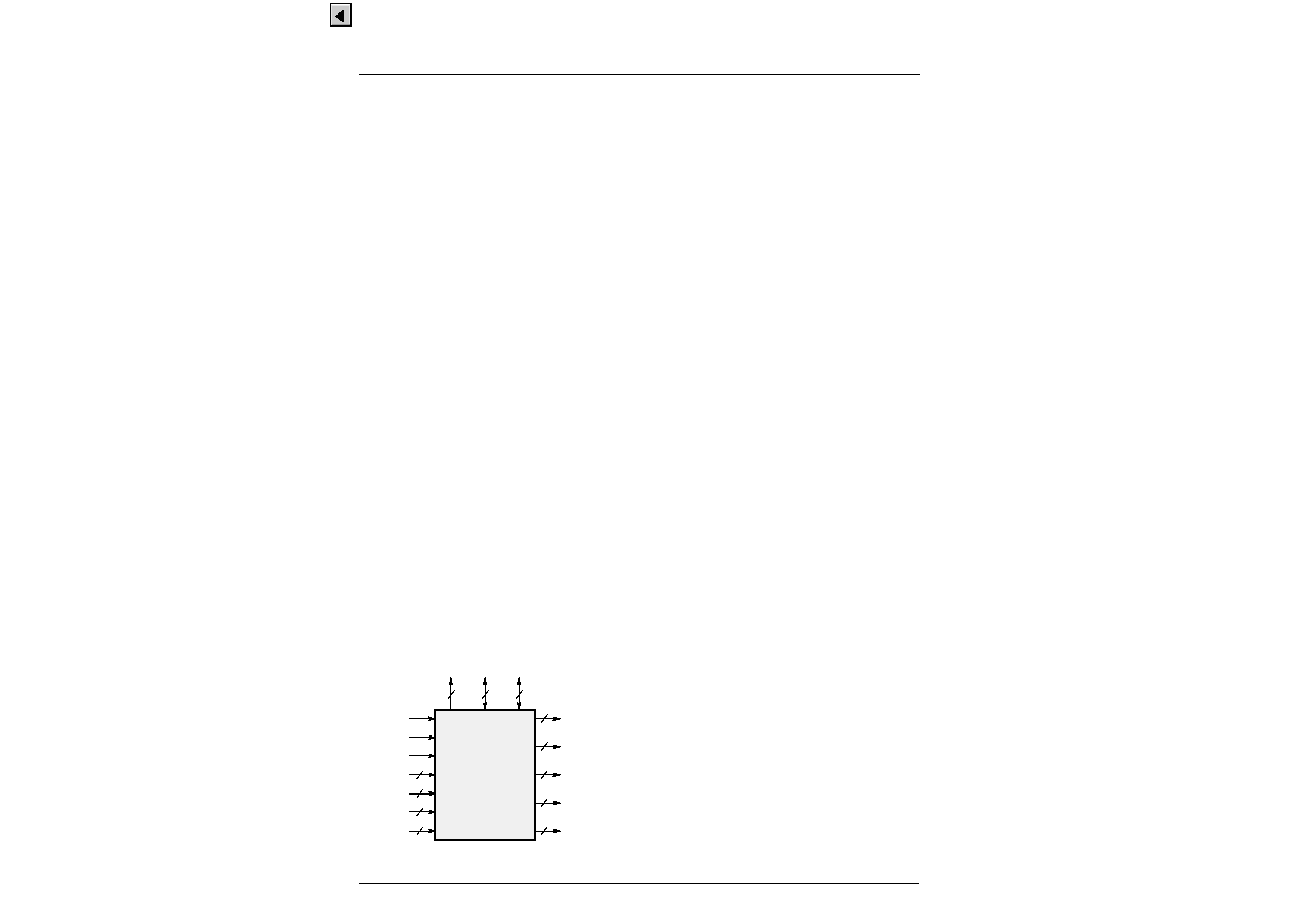
Fig. 2≠1: Main I/O signals of the MSP 34x0D
2.2. DSP Section (Audio Baseband Processing)
≠ flexible selection of audio sources to be processed
≠ two digital input and one output interface via I
2
S bus
for external DSP processors, featuring surround
sound, ADR etc.
≠ digital interface to process ADR (ASTRA Digital
Radio) together with DRP 3510A
≠ performance of all deemphasis systems including
adaptive Wegener Panda 1 without external compo-
nents or controlling
≠ digitally performed FM identification decoding and
dematrixing
≠ digital baseband processing: volume, bass, treble,
5-band equalizer, loudness, pseudostereo, and
basewidth enlargement
≠ simple controlling of volume, bass, treble, equalizer
etc.
2.3. Analog Section
≠ four selectable analog pairs of audio baseband
inputs (= four SCART inputs)
input level:
2 V
RMS
,
input impedance:
25 k
≠ one selectable analog mono input (i.e. AM sound):
input level:
2 V
RMS
,
input impedance:
15 k
≠ two high-quality A/D converters, S/N-Ratio:
85 dB
≠ 20 Hz to 20 kHz bandwidth for
SCART-to-SCART copy facilities
≠ MAIN (loudspeaker) and AUX (headphones): two
pairs of fourfold oversampled D/A-converters
output level per channel: max. 1.4 V
RMS
output resistance: max. 5 k
S/N-ratio:
85 dB at maximum volume
max. noise voltage in mute mode:
10
µ
V
(BW: 20 Hz ...16 kHz)
≠ two pairs of fourfold oversampled D/A converters
supplying two selectable pairs of SCART outputs.
output level per channel: max. 2 V
RMS
,
output resistance: max. 0.5 k
,
S/N-Ratio:
85 dB (20 Hz ... 16 kHz)
Loudspeaker
OUT
Subwoofer
OUT
Headphones
OUT
SCART1
OUT
SCART2
OUT
MSP 34x0D
2
2
2
2
1
2
3
5
ADR
I
2
S
I
2
C
Sound IF 1
Sound IF 2
MONO IN
SCART1 IN
SCART2 IN
SCART3 IN
SCART4 IN
2
2
2
2
PRELIMINARY DATA SHEET
MSP 34x0D
Micronas
7
3. Application Fields of the MSP 34x0D
In the following sections, a brief overview of the two
main TV sound standards, NICAM 728 and German
FM-Stereo, demonstrates the complex requirements of
a multistandard audio IC.
3.1. NICAM plus FM/AM-Mono
According to the British, Scandinavian, Spanish, and
French TV standards, high-quality stereo sound is
transmitted digitally. The systems allow two high-qual-
ity digital sound channels to be added to the already
existing FM/AM channel. The sound coding follows the
format of the so-called Near Instantaneous Compand-
ing System (NICAM 728). Transmission is performed
using Differential Quadrature Phase Shift Keying
(DQPSK). Table 3≠2 provides some specifications of
the sound coding (NICAM); Table 3≠3 offers an over-
view of the modulation parameters.
In the case of NICAM/FM (AM) mode, there are three
different audio channels available: NICAM A,
NICAM B, and FM/AM-Mono. NICAM A and B may
belong either to a stereo or to a dual-language trans-
mission. Information about operation mode and the
quality of the NICAM signal can be read by the CCU
via the control bus. In the case of low quality (high bit-
error rate), the CCU may decide to switch to the ana-
log FM/AM-Mono sound. Alternatively, an automatic
NICAM-FM/AM switching may be applied.
3.2. German 2-Carrier System (Dual-FM System)
Since September 1981, stereo and dual-sound pro-
grams have been transmitted in Germany using the
2-carrier system. Sound transmission consists of the
already existing first sound carrier and a second sound
carrier additionally containing an identification signal.
More details of this standard are given in Tables 3≠1
and 3≠4. For D/K and M-Korea, very similar systems
are used.
Note: NICAM demodulation cannot be done with the MSP 3400D
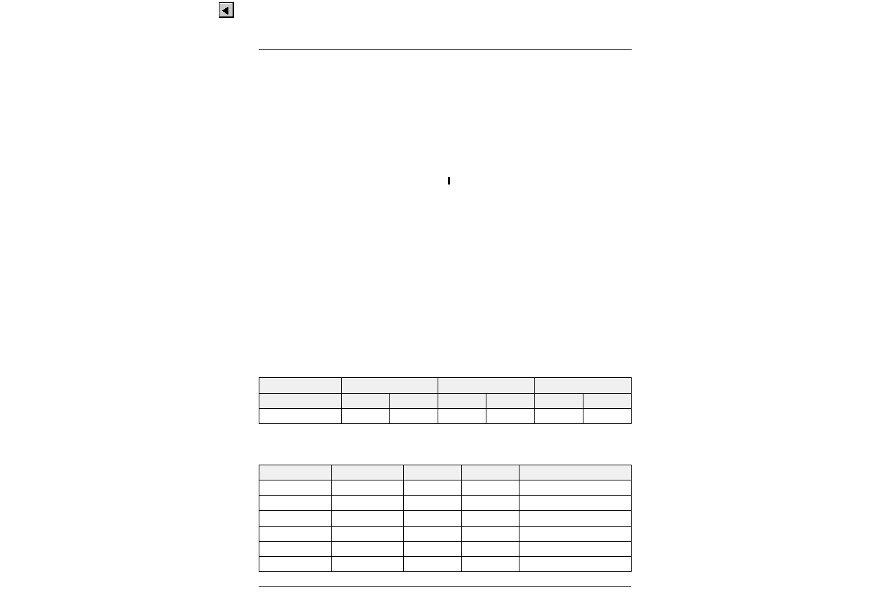
Table 3≠1: TV standards
TV System
Position of Sound
Carrier /MHz
Sound
Modulation
Color System
Country
B/G
5.5/5.7421875
FM-Stereo
PAL
Germany
B/G
5.5/5.85
FM-Mono/NICAM
PAL
Scandinavia, Spain
L
6.5/5.85
AM-Mono/NICAM
SECAM-L
France
I
6.0/6.552
FM-Mono/NICAM
PAL
UK
D/K
6.5/6.2578125 D/K1
6.5/6.7421875 D/K2
6.5/5.85 D/K-NICAM
FM-Stereo
FM-Mono/NICAM
SECAM-East
USSR
Hungary
M
M-Korea
4.5
4.5/4.724212
FM-Mono
FM-Stereo
NTSC
USA
Korea
Satellite
Satellite
6.5
7.02/7.2
FM-Mono
FM-Stereo
PAL
PAL
Europe (ASTRA)
Europe (ASTRA)
MSP 34x0D
PRELIMINARY DATA SHEET
8
Micronas
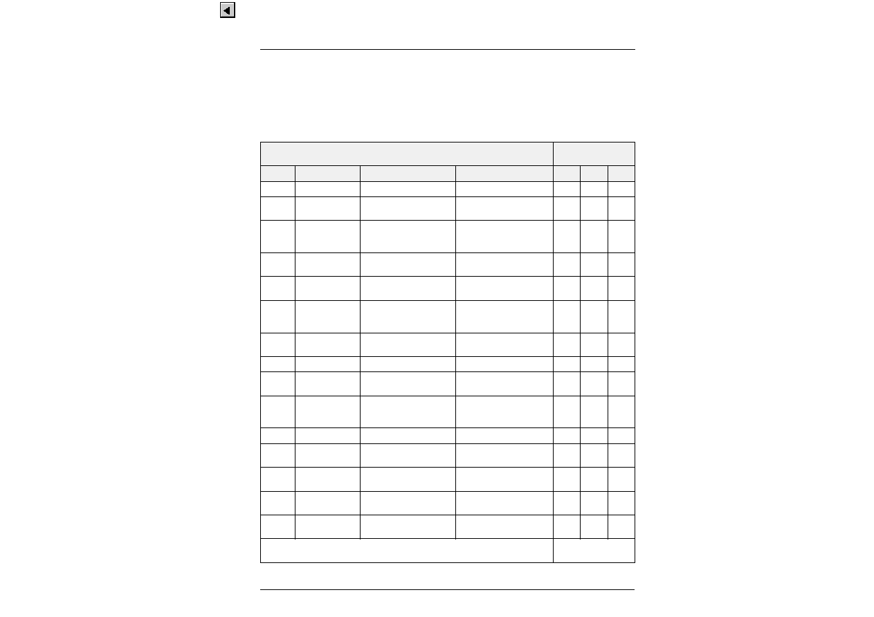
Table 3≠2: Summary of NICAM 728 sound coding characteristics
Characteristics
Values
Audio sampling frequency
32 kHz
Number of channels
2
Initial resolution
14 bits/sample
Companding characteristics
near instantaneous, with compression to 10 bits/sample in 32-sample
(1 ms) blocks
Coding for compressed samples
2's complement
Preemphasis
CCITT recommendation J.17 (6.5 dB attenuation at 800 Hz)
Audio overload level
+12 dBm measured at the unity gain frequency of the preemphasis
network (2 kHz)
Table 3≠3: Summary of NICAM 728 sound modulation parameters
Specification
I
B/G
L
D/K
Carrier frequency of
digital sound
6.552 MHz
5.85 MHz
5.85 MHz
5.85 MHz
Transmission rate
728 kbit/s
Type of modulation
Differentially encoded quadrature phase shift keying (DQPSK)
Spectrum shaping
Roll-off factor
by means of Roll-off filters 1.0
1.0
0.4
0.4
0.4
Carrier frequency of
analog sound component
6.0 MHz
FM mono
5.5 MHz
FM mono
6.5 MHz AM mono
6.5 MHz
FM-Mono
terrestrial
cable
Power ratio between
vision carrier and
analog sound carrier
10 dB
13 dB
10 dB
16 dB
13 dB
Power ratio between
analog and modulated
digital sound carrier
10 dB
7 dB
17 dB
11 dB
Hungary
Poland
12 dB
7 dB

PRELIMINARY DATA SHEET
MSP 34x0D
Micronas
9
Fig. 3≠1: Typical MSP 34x0D application
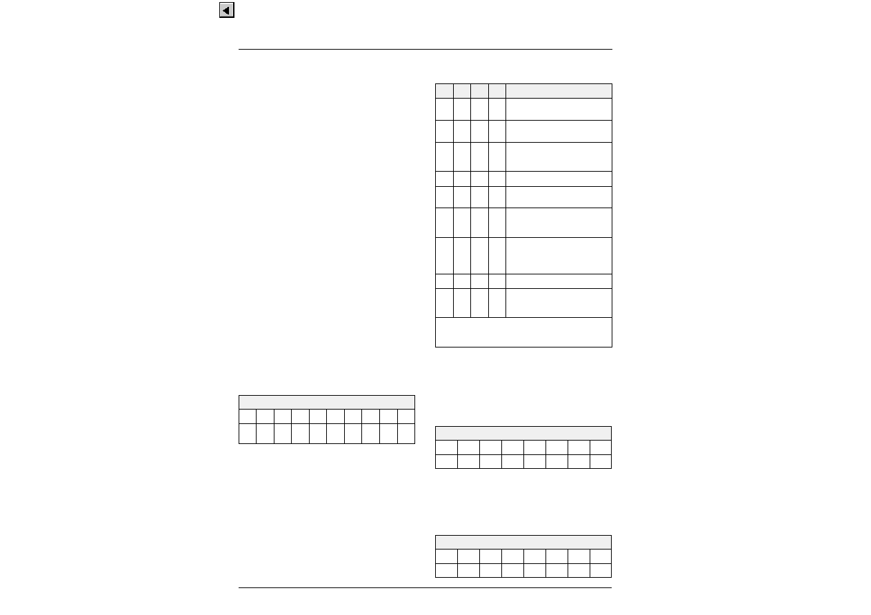
Table 3≠4: Key parameters for B/G, D/K, and M 2-carrier sound system
Sound Carriers
Carrier FM1
Carrier FM2
B/G
D/K
M
B/G
D/K
M
Vision/sound power ratio
13 dB
20 dB
Sound bandwidth
40 Hz to 15 kHz
Preemphasis
50
µ
s
75
µ
s
50
µ
s
75
µ
s
Frequency deviation
±
50 kHz
±
25 kHz
±
50 kHz
±
25 kHz
Sound Signal Components
Mono transmission
mono
mono
Stereo transmission
(L+R)/2
(L+R)/2
R
(L
-
R)/2
Dual-sound transmission
language A
language B
Identification of Transmission Mode on Carrier FM2
Pilot carrier frequency in kHz
54.6875
55.0699
Type of modulation
AM
Modulation depth
50 %
Modulation frequency
mono:
unmodulated
stereo: 117.5 Hz
dual:
274.1 Hz
149.9 Hz
276.0 Hz
33
34
39 MHz
5
9 MHz
According to the mixing characteristics
of the sound IF mixer, the sound IF
filter may be omitted.
Loudspeaker
Subwoofer
Headphone
SCART
Outputs
2
2
SCART2
SCART1
MSP 34x0D
I
2
S2
ADR
I
2
S1
ADR
Decoder
DRP3510A
Dolby
Pro Logic
Processor
DPL35xxA
2
2
2
2
SCART1
SCART2
SCART3
SCART4
1
Mono
SAW Filter
Sound IF Filter
Sound
IF
Mixer
Vision
Demo-
dulator
Tuner
SCART
Inputs
Composite
Video

MSP 34x0D
PRELIMINARY DATA SHEET
10
Micronas
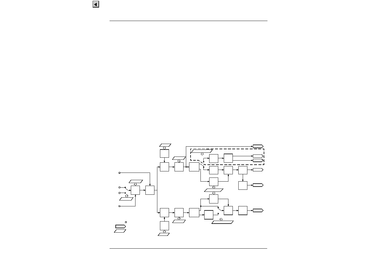
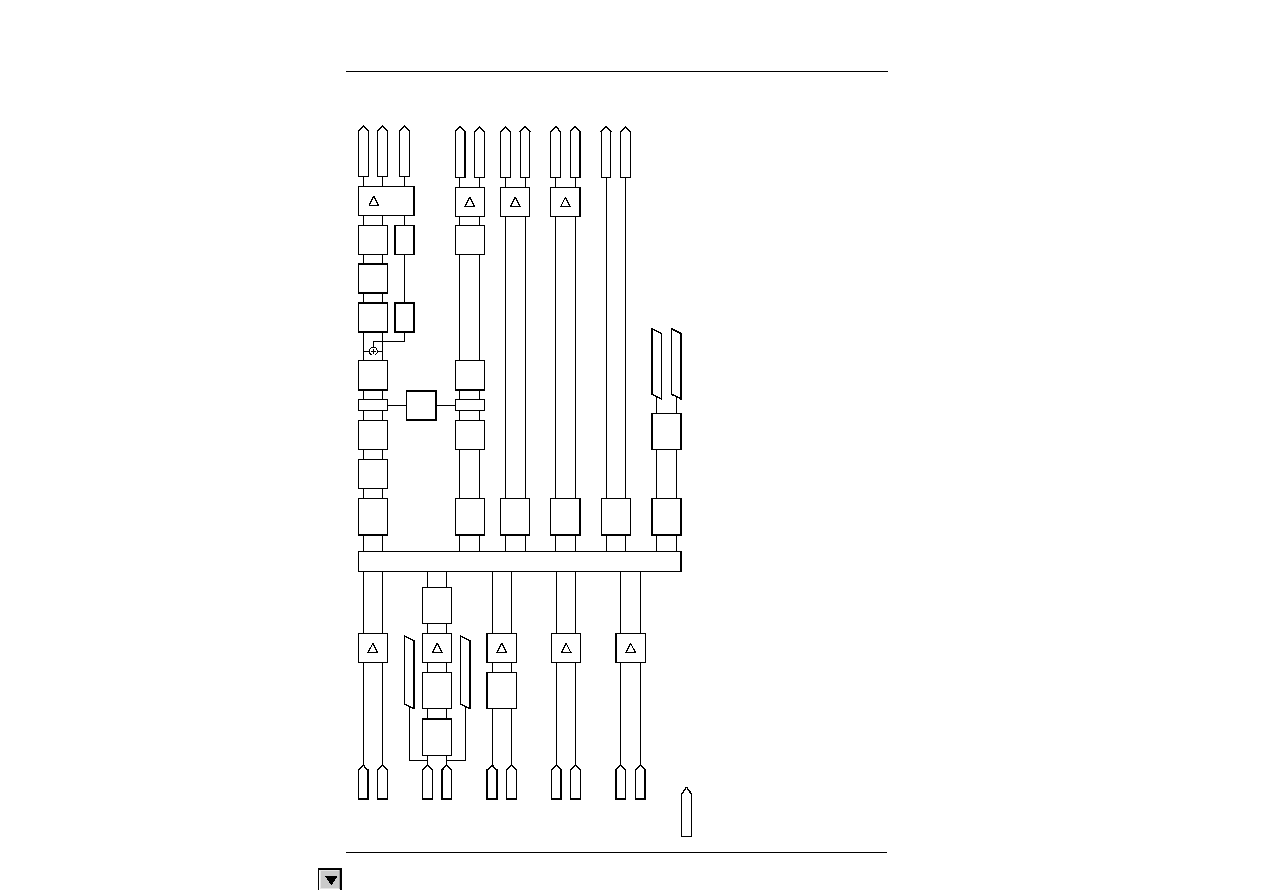
4. Architecture of the MSP 34x0D
Fig. 4≠1 shows a simplified block diagram of the IC. Its
architecture is split into three main functional blocks:
1. demodulator and NICAM decoder section
2. digital signal processing (DSP) section performing
audio baseband processing
3. analog section containing two A/D-converters,
nine D/A-converters, and SCART Switching Facili-
ties.
4.1. Demodulator and NICAM Decoder Section
4.1.1. Analog Sound IF ≠ Input Section
The input pins ANA_IN1+, ANA_IN2+, and ANA_IN
-
offer the possibility to connect two different sound IF
(SIF) sources to the MSP 34x0D. By means of bit [8] of
AD_CV (see Table 6≠5 on page 25), either terrestrial
or satellite sound IF signals can be selected. The ana-
log-to-digital conversion of the preselected sound IF
signal is done by an A/D converter whose output is
used to control an analog automatic gain circuit (AGC)
providing an optimal level for a wide range of input lev-
els. It is possible to switch between automatic gain
control and a fixed (setable) input gain. In the optimal
case, the input range of the A/D converter is com-
pletely covered by the sound IF source. Some combi-
nations of SAW filters and sound IF mixer ICs, how-
ever, show large picture components on their outputs.
In this case, filtering is recommended. It was found,
that the high-pass filters formed by the coupling capac-
itors at pins ANA_IN1+ and ANA_IN2+ and the IF
impedance (as shown in the application diagram) are
sufficient in most cases.
Fig. 4≠1: Architecture of the MSP 34x0D
Sound IF
ANA_IN1+
ANA_IN2+
Mono
MONO_IN
SC1_IN_L
SCART1
SC1_IN_R
SC2_IN_L
SCART2
SC2_IN_R
SC3_IN_L
SCART3
SC3_IN_R
SC4_IN_L
SC4_IN_R
SCART4
Demodulator
& NICAM
Decoder
SCART Switching Facilities
A/D
A/D
D/A
D/A
D/A
D/A
D/A
D/A
D/A
D/A
D/A
2
IDENT
SCARTL
SCARTR
NICAM B
NICAM A
FM2
I2S1/2L/R
FM1/AM
I2S_L/R
LOUD-
SPEAKER L
LOUD-
SPEAKER R
SCART1_L
SCART1_R
SCART2_L
SCART2_R
DSP
HEADPHONE R
HEADPHONE L
SUBWOOFER
I
2
S Interface
Crystal PLL
ADR-Bus
I2S_DA_IN1
I2S_DA_OUT
I2S_DA_IN2
I2S_WS
I2S_CL
XTAL_OUT
AUD_CL_OUT
XTAL_IN
D_CTR_OUT0/1
DACM_L
Loudspeaker
DACM_R
DACM_SUB
Subwoofer
Headphone
DACA_L
DACA_R
SC1_OUT_L
SC1_OUT_R
SC2_OUT_L
SC2_OUT_R
SCART 2
SCART 1
PRELIMINARY DATA SHEET
MSP 34x0D
Micronas
11
4.1.2. Quadrature Mixers
The digital input coming from the integrated A/D con-
verter may contain audio information at a frequency
range of theoretically 0 to 9 MHz corresponding to the
selected standards. By means of two programmable
quadrature mixers, two different audio sources, for
example NICAM and FM-Mono, may be shifted into
baseband position. In the following, the two main
channels are provided to process either:
≠ NICAM (MSP-Ch1) and FM/AM mono (MSP-Ch2)
simultaneously or, alternatively:
≠ FM-Mono (Ch2)
≠ FM2 (MSP-Ch1) and FM1 (MSP-Ch2).
Two programmable registers, to be divided up into a
low and a high part, determine frequency of the oscilla-
tor, which corresponds to the frequency of the desired
audio carrier.
4.1.3. Low-pass Filtering Block
for Mixed Sound IF Signals
Data shaping and/or FM bandwidth limitation is per-
formed by a linear phase finite impulse response (FIR)
filter. Just like the oscillators' frequency, the filter coeffi-
cients are programmable and are written into the IC by
the CCU via the control bus. Thus, for example, differ-
ent NICAM versions can easily be implemented. Two
not necessarily different sets of coefficients are
required, one for MSP-Ch1 (NICAM or FM2) and one
for MSP-Ch2 (FM1 = FM-mono). In a corresponding
table several coefficient sets are proposed.
Fig. 4≠2: Architecture of demodulator and NICAM decoder section
Phase and
AM Dis-
crimination
MSP sound IF channel 1
(MSP-Ch1: FM2, NICAM)
MSP sound IF channel 2
(MSP-Ch2: FM1, AM)
VREFTOP
ANA_IN1+
ANA_IN2+
ANA_IN-
AD_CV[8]
AD_CV[7:1]
AGC
AD
DCO1
Oscillator
Mixer
FIR1
Lowpass
MODE_REG[6]
Amplitude
DQPSK
Decoder
Phase
Differen-
tiator
Carrier
Detect
AD_CV[9]
Mute
NICAM
Decoder
Mixer
Lowpass
ADR
NICAMA
NICAMB
FM2
IDENT
Carrier
Detect
Mute
Lowpass
FM1/AM
MODE_REG[8]
Differen-
tiator
Phase
FIR2
Lowpass
Phase and
AM Dis-
crimination
Amplitude
Mixer
Oscillator
DCO2
Pins
Demodulator Write Registers
FRAME
NICAMA
DCO2
Internal signal lines (see fig. 4≠2)
MSP3410D only

MSP 34x0D
PRELIMINARY DATA SHEET
12
Micronas
4.1.4. Phase and AM Discrimination
The filtered sound IF signals are demodulated by
means of the phase and amplitude discriminator block.
On the output, the phase and amplitude is available for
further processing. AM signals are derived from the
amplitude information, whereas the phase information
serves for FM and NICAM (DQPSK) demodulation.
4.1.5. Differentiators
FM demodulation is completed by differentiating the
phase information output.
4.1.6. Low-pass Filter Block
for Demodulated Signals
The demodulated FM and AM signals are further low-
pass filtered and decimated to a final sampling fre-
quency of 32 kHz. The usable bandwidth of the final
baseband signals is about 15 kHz.
4.1.7. High-Deviation FM Mode
By means of MODE_REG [9], the maximum FM devi-
ation can be extended to approximately
±
360 kHz.
Since this mode can be applied only for the MSP
sound IF channel 2, the corresponding matrices in the
baseband processing must be set to sound A. Apart
from this, the coefficient sets 380 kHz FIR2 or 500 kHz
FIR2 must be chosen for the FIR2. In relation to the
normal FM mode, the audio level of the high-deviation
mode is reduced by 6 dB. The FM prescaler should be
adjusted accordingly. In high-deviation FM mode, nei-
ther FM-Stereo nor FM identification nor NICAM pro-
cessing is possible simultaneously.
4.1.8. FM Carrier Mute Function
in the Dual-Carrier FM Mode
To prevent noise effects or FM identification problems
in the absence of one of the two FM carriers, the
MSP 34x0D offers a carrier detection feature, which
must be activated by means of AD_CV[9]. If no FM
carrier is available at the MSPD channel 1, the corre-
sponding channel FM2 is muted. If no FM carrier is
available at the MSPD channel 2, the corresponding
channel FM1 is muted.
4.1.9. DQPSK Decoder
In case of NICAM mode, the phase samples are
decoded according the DQPSK-coding scheme. The
output of this block contains the original NICAM bit-
stream.
4.1.10. NICAM Decoder
Before any NICAM decoding can start, the MSP must
lock to the NICAM frame structure by searching and
synchronizing to the so-called frame alignment words
(FAW).
To reconstruct the original digital sound samples, the
NICAM bitstream has to be descrambled, deinter-
leaved, and rescaled. Also, bit-error detection and cor-
rection (concealment) is performed in this block.
To facilitate the Central Control Unit CCU to switch the
(e.g.) TV set to the actual sound mode, control infor-
mation on the NICAM mode and bit error rate are sup-
plied by the NICAM decoder. It can be read out via the
I
2
C bus.
An automatic switching facility (AUTO_FM) between
NICAM and FM/AM reduces the amount of
CCU instructions in case of bad NICAM reception.

PRELIMINARY DATA SHEET
MSP 34x0D
Micronas
13
4.2. Analog Section
4.2.1. SCART Switching Facilities
The analog input and output sections include full matrix
switching facilities, which are shown in Fig. 4≠3. To
design a TV set with four pairs of SCART inputs and
two pairs of SCART outputs, no external switching
hardware is required.
The switches are controlled by the ACB bits defined in
the audio processing interface (see section 7.3.18. on
page 47).
Fig. 4≠3: SCART switching facilities (see 7.3.18.).
Switching positions show the default configuration
after power-on reset
4.2.2. Stand-by Mode
If the MSP 34x0D is switched off by first pulling
STANDBYQ low, and then disconnecting the 5 V, but
keeping the 8 V power supply (`Stand-by'-mode), the
switches S1, S2, and S3 (see Fig. 4≠3) maintain their
position and function. This facilitates the copying from
selected SCART inputs to SCART outputs in the
TV set's stand-by mode.
In case of power-on start or starting from stand-by, the
IC switches automatically to the default configuration,
shown in Fig. 4≠3. This action takes place after the
first I
2
C transmission into the DSP part. By transmitting
the ACB register first, the individual default setting
mode of the TV set can be defined.
4.3. DSP Section (Audio Baseband Processing)
All audio baseband functions are performed by digital
signal processing (DSP). The DSP functions are
grouped into three processing parts: input preprocess-
ing, channel source selection, and channel postpro-
cessing (see Fig. 4≠5 and section 7.).
The input preprocessing is intended to prepare the
various signals of all input sources in order to form a
standardized signal at the input to the channel selec-
tor. The signals can be adjusted in volume, are pro-
cessed with the appropriate deemphasis, and are
dematrixed if necessary.
Having prepared the signals that way, the channel
selector makes it possible to distribute all possible
source signals to the desired output channels.
The ability to route in an external coprocessor for spe-
cial effects, like surround processing and sound field
processing, is of special importance. Routing can be
done with each input source and output channel via
the I
2
S inputs and outputs.
All input and output signals can be processed simulta-
neously with the exception that FM2 cannot be pro-
cessed at the same time as NICAM. FM identification
and adaptive deemphasis are also not possible simul-
taneously. Note, that the NICAM input signals are only
available in the MSP 3410D version.
4.3.1. Dual-Carrier FM Stereo/Bilingual Detection
For the terrestrial dual-FM carrier systems, audio infor-
mation can be transmitted in three modes: mono, ste-
reo, or bilingual. To obtain information about the current
audio operation mode, the MSP 34x0D detects the so-
called identification signal. Information is supplied via
the Stereo Detection Register to an external CCU.
Fig. 4≠4: Stereo/bilingual detection
A
D
D
A
A
D
SCART_IN
SC1_IN_L/R
SC2_IN_L/R
SC3_IN_L/R
SC4_IN_L/R
MONO_IN
ACB[5,9,8]
Mute
S1
SCARTL/R
to Audio Baseband
Processing (DSP_IN)
ACB
[6,11,10]
SCART_OUT
SC1_OUT_L/R
S2
ACB
[7,13,12]
Mute
SC2_OUT_L/R
from Audio Baseband
Processing (DSP_OUT)
SCART1_L/R
SCART2_L/R
Mute
S3
SCART_OUT
IDENT
AM
Demodu-
lation
Stereo
Detection
Filter
Bilingual
Detection
Filter
Level
Detect
Level
Detect
-
Stereo
Detection
Register
MSP
34x0
D
PR
EL
I
M
IN
A
R
Y D
A
TA
SH
EE
T
14
M
i
c
r
onas
C
hannel Sour
ce
Select
Fig. 4≠5: Audio baseband processing (DSP firmware)
Analog
Inputs
SCARTL
SCARTR
Demodulated
IF
Inputs
I
2
S Bus
Inputs
Prescale
SCART
DC level readout FM1
FM1/AM
FM2
Adaptive
Deemphasis
Deemphasis
50/75
µ
s
J17
Prescale
FM/AM
FM-Matrix
DC level readout FM2
Loudspeaker
Channel
Matrix
Prescale
Prescale
I
2
S1
Deemphasis
J17
NICAMB
NICAMA
I
2
S1L
I
2
S1R
Prescale
I
2
S2
I
2
S2L
I
2
S2R
I
2
S
Channel
Matrix
NICAM
NICAMA
Quasi-Peak
Channel
Matrix
SCART2
Channel
Matrix
SCART1
Channel
Matrix
Headphone
Channel
Matrix
AVC
Bass/
Treble
or
Equalizer
Beeper
Bass/
Treble
Loudness
Loudness
Quasi-Peak
Detector
Quasi peak readout L
Quasi peak readout R
Comple-
mentary
Highpass
Lowpass
Spatial
Effects
Balance
Level
Adjust
Balance
Volume
Volume
Volume
Loudspeaker L
Loudspeaker R
Subwoofer
Volume
Loudspeaker
Outputs
Headphone
Outputs
SCART
Outputs
I
2
S
Outputs
I
2
SR
I
2
SL
SCART2_R
SCART2_L
SCART1_R
SCART1_L
Headphone R
Headphone L
Internal signal lines (see Fig. 4≠2 and Fig. 4≠3)

PRELIMINARY DATA SHEET
MSP 34x0D
Micronas
15
4.4. Audio PLL and Crystal Specifications
The MSP 34x0D requires a 18.432 MHz (12 pF, paral-
lel) crystal. The clock supply of the whole system
depends on the MSP 34x0D operation mode:
1. FM-Stereo, FM-Mono:
The system clock runs free on the crystal's
18.432 MHz.
2. NICAM:
An integrated clock PLL uses the 364 kHz baud
rate, accomplished in the NICAM demodulator block
to lock the system clock to the bit rate, respectively,
32-kHz sampling rate of the NICAM transmitter. As
a result, the whole audio system is supplied with a
controlled 18.432 MHz clock.
3. I
2
S slave operation:
In this case, the system clock is locked to a synchro-
nizing signal (I2S_CL, I2S_WS) supplied by the
coprocessor chip.
Remark on using the crystal:
External capacitors at each crystal pin to ground are
required (see General Crystal Recommendations on
page 69).
4.5. ADR Bus Interface
For the ASTRA Digital Radio System (ADR), the
MSP 34x0D performs preprocessing, as there are car-
rier selection and filtering. Via the 3-line ADR bus, the
resulting signals are transferred to the DRP 3510A,
where the source decoding is performed. To be pre-
pared for an upgrade to ADR with an additional DRP
board, the following lines of MSP 34x0D should be
provided on a feature connector:
≠ AUD_CL_OUT
≠ I2S_DA_IN1 or I2S_DA_IN2
≠ I2S_DA_OUT
≠ I2S_WS
≠ I2S_CLK
≠ ADR_CL
≠ ADR_WS
≠ ADR_DA
4.6. Digital Control Output Pins
The static level of two output pins of the MSP 34x0D
(D_CTR_OUT0/1) is switchable between HIGH and
LOW by means of the I
2
C bus. This enables the con-
trolling of external hardware-controlled switches or
other devices via I
2
C bus (see section 7.3.18. on page
47).
Table 4≠1: Some examples for recommended channel assignments for demodulator and audio processing part
Mode
MSP Sound IF-
Channel 1
MSP Sound IF-
Channel 2
FM-
Matrix
Channel-
Select
Channel
Matrix
B/G-Stereo
FM2 (5.74 MHz): R
FM1 (5.5 MHz): (L+R)/2
B/G Stereo
Speakers: FM
Stereo
B/G-Bilingual
FM2 (5.74 MHz): Sound B
FM1 (5.5 MHz): Sound A
No Matrix
Speakers: FM
H. Phone: FM
Speakers: Sound A
H. Phone: Sound B
NICAM-I-ST/
FM-mono
NICAM (6.552 MHz)
FM (6.0 MHz): mono
No Matrix
Speakers: NICAM
H. Phone: FM
Speakers: Stereo
H. Phone: Sound A
Sat-Mono
not used
FM (6.5 MHz): mono
No Matrix
Speakers: FM
Sound A
Sat-Stereo
7.2 MHz: R
7.02 MHz:
L
No Matrix
Speakers: FM
Stereo
Sat-Bilingual
7.38 MHz: Sound C
7.02 MHz:
Sound A
No Matrix
Speakers: FM
H. Phone: FM
Speakers: Sound A
H. Phone: Sound B=C
Sat-High Dev.
Mode
don't care
6.552 MHz
No Matrix
Speakers: FM
H. Phone: FM
Speakers: Sound A
H. Phone: Sound A

MSP 34x0D
PRELIMINARY DATA SHEET
16
Micronas
4.7. I
2
S Bus Interface
By means of this standardized interface, additional
feature processors can be connected to the
MSP 34x0D. Two possible formats are supported: The
standard mode (MODE_REG[4]=0) selects the SONY
format, where the I2S_WS signal changes at the word
boundaries. The so-called PHILIPS format, which is
characterized by a change of the I2S_WS signal one
I2S_CL period before the word boundaries, is selected
by setting MODE_REG[4]=1.
The MSP 34x0D normally serves as the master on the
I
2
S interface. Here, the clock and word strobe lines are
driven by the MSP 34x0D. By setting
MODE_REG[3]=1, the MSP 34x0D is switched to a
slave mode. Now, these lines are input to the
MSP 34x0D and the master clock is synchronized to
576 times the I2S_WS rate (32 kHz). NICAM operation
is not possible in this mode.
The I
2
S bus interface consists of five pins:
1. I2S_DA_IN1, I2S_DA_IN2:
For input, four channels (two channels per line,
2*16 bits) per sampling cycle (32 kHz) are transmit-
ted.
2. I2S_DA_OUT:
For output, two channels (2*16 bits) per sampling
cycle (32 kHz) are transmitted.
3. I2S_CL:
Gives the timing for the transmission of I
2
S serial
data (1.024 MHz).
4. I2S_WS:
The I2S_WS word strobe line defines the left and
right sample.
A precise I
2
S timing diagram is shown in Fig. 4≠6.
Fig. 4≠6: I
2
S bus timing diagram
(Data: MSB first)
R LSB L LSB
R LSB L LSB
16 bit right channel
L LSB
L LSB
R MSB
R MSB
Detail C
PHILIPS Mode
SONY Mode
I2S_WS
I2S_CL
I2S_DAIN
Detail A
PHILIPS Mode
SONY Mode
Detail B
PHILIPS/SONY Mode programmable by MODE_REG[4]
R LSB
R LSB L MSB
L MSB
I2S_DAOUT
16 bit right channel
16 bit left channel
16 bit left channel
F
I2SWS
I2S_CL
Detail C
I2S_WS as INPUT
I2S_WS as OUTPUT
1/F
I2SCL
T
I2SWS1
T
I2SWS2
T
I2S5
T
I2S6
Detail A,B
I2S_CL
I2S_DA_IN
I2S_DA_OUT
T
I2S1
T
I2S2
T
I2S3
T
I2S4
PRELIMINARY DATA SHEET
MSP 34x0D
Micronas
17
5. I
2
C Bus Interface: Device and Subaddresses
As a slave receiver, the MSP 34x0D can be controlled
via I
2
C bus. Access to internal memory locations is
achieved by subaddressing. The demodulator and the
DSP processor parts have two separate subaddress-
ing register banks.
In order to allow for more MSP 34x0D ICs to be con-
nected to the control bus, an ADR_SEL pin has been
implemented. With ADR_SEL pulled to HIGH, LOW, or
left open, the MSP 34x0D responds to changed device
addresses. Thus, three identical devices can be
selected.
By means of the RESET bit in the CONTROL register,
all devices with the same device address are reset.
The IC is selected by asserting a special device
address in the address part of an I
2
C transmission. A
device address pair is defined as a write address (80,
84, or 88
hex
) and a read address (81, 85, or 89
hex
)
(see Table 5≠1). Writing is done by sending the device
write address, followed by the subaddress byte, two
address bytes, and two data bytes. Reading is done by
sending the device write address, followed by the sub-
address byte and two address bytes. Without sending
a stop condition, reading of the addressed data is com-
pleted by sending the device read address (81, 85, or
89
hex
) and reading two bytes of data (see Fig. 5≠1:
"I
2
C Bus Protocol" and section 5.2. "Proposal for
MSP 34x0D I
2
C Telegrams").
Due to the internal architecture of the MSP 34x0D, the
IC cannot react immediately to an I
2
C request. The typ-
ical response time is about 0.3 ms for the DSP proces-
sor part and 1 ms for the demodulator part if NICAM
processing is active. If the receiver (MSP) can't receive
another complete byte of data until it has performed
some other function; for example, servicing an internal
interrupt, it can hold the clock line I2C_CL LOW to
force the transmitter into a wait state. The positions
within a transmission where this may happen are indi-
cated by 'Wait' in section 5.1. The maximum wait
period of the MSP during normal operation mode is
less than 1 ms.
I
2
C bus error caused by MSP hardware problems:
In case of any internal error, the MSPs wait period is
extended to 1.8 ms. Afterwards, the MSP does not
acknowledge (NAK) the device address. The data line
will be left HIGH by the MSP and the clock line will be
released. The master can then generate a STOP con-
dition to abort the transfer.
By means of NAK, the master is able to recognize the
error state and to reset the IC via I
2
C bus. While trans-
mitting the reset protocol (see section 5.2.4. on page
19) to `CONTROL', the master must ignore the not-
acknowledge bits (NAK) of the MSP.
A general timing diagram of the I
2
C Bus is shown in
Fig. 5≠2 on page 19.
Table 5≠1: I
2
C Bus Device Addresses
ADR_SEL
Low
High
Left Open
Mode
Write
Read
Write
Read
Write
Read
MSP device address
80 hex
81 hex
84 hex
85 hex
88 hex
89 hex
Table 5≠2: I
2
C Bus Subaddresses
Name
Binary Value
Hex Value
Mode
Function
CONTROL
0000 0000
00
W
software reset
TEST
0000 0001
01
W
only for internal use
WR_DEM
0001 0000
10
W
write address demodulator
RD_DEM
0001 0001
11
W
read address demodulator
WR_DSP
0001 0010
12
W
write address DSP
RD_DSP
0001 0011
13
W
read address DSP

MSP 34x0D
PRELIMINARY DATA SHEET
18
Micronas
5.1. Protocol Description
Write to DSP or Demodulator
Read from DSP or Demodulator
Write to Control or Test Registers
Note: S =
I
2
C bus Start Condition from master
P =
I
2
C bus Stop Condition from master
ACK = Acknowledge-Bit: LOW on I2C_DA from slave (
=
MSP, gray)
or master (
=
CCU, hatched)
NAK = Not-Acknowledge Bit: HIGH on I2C_DA from master (
=
CCU, hatched) to indicate `End of Read'
or from MSP indicating internal error state
Wait = I
2
C clock line held low by the slave (
=
MSP) while interrupt is serviced (
<
1.8 ms)
Fig. 5≠1: I
2
C bus protocol
(MSB first; data must be stable while clock is high)
Table 5≠3: Control Register (Subaddress: 00 hex)
Name
Subaddress
MSB
14
13..1
LSB
CONTROL
00 hex
1 : RESET
0 : normal
0
0
0
S
write
device
address
Wait
ACK
subaddr
ACK
addr byte
high
ACK
addr byte
low
ACK
data byte
high
ACK
data byte
low
ACK
P
S
write
device
address
Wait
ACK
subaddr
ACK
addr byte
high
ACK
addr byte
low
ACK
S
read
device
address
Wait
ACK
data byte
high
ACK
data byte
low
NAK
P
S
write
device
address
Wait
ACK
subaddr
ACK
data byte high
ACK
data byte low
ACK
P
1
0
S
P
I2C_DA
I2C_CL

PRELIMINARY DATA SHEET
MSP 34x0D
Micronas
19
(Data: MSB first)
Fig. 5≠2: I
2
C bus timing diagram
5.2. Proposal for MSP 34x0D I
2
C Telegrams
5.2.1. Symbols
daw
write device address
dar
read device address
<
start condition
>
stop condition
aa
address byte
dd
data byte
5.2.2. Write Telegrams
<daw 00 d0 00>
write to CONTROL register
<daw 10 aa aa dd dd>
write data into demodulator
<daw 12 aa aa dd dd>
write data into DSP
5.2.3. Read Telegrams
<daw 11 aa aa <dar dd dd>
read data from demodulator
<daw 13 aa aa <dar dd dd>
read data from DSP
5.2.4. Examples
<80 00 80 00>
RESET MSP statically
<80 00 00 00>
clear RESET
<80 12 00 08 01 20>
set loudspeaker channel source
to NICAM and matrix to STEREO
I2C_CL
I2C_DA as input
I2C_DA as output
T
I2C1
T
I2C5
T
I2C6
T
I2C2
T
I2C4
T
I2C3
f
I2C
T
I2COL2
T
I2COL1
1

MSP 34x0D
PRELIMINARY DATA SHEET
20
Micronas
5.3. Start-Up Sequence: Power-Up and I
2
C-Controlling
After power-on or RESET (see Fig. 5≠3), the IC is in
an inactive state. The CCU has to transmit the
required coefficient set for a given operation via the
I
2
C bus. Initialization should start with the demodulator
part. If required for any reason, the audio processing
part can be loaded before the demodulator part.
Fig. 5≠3: Power-up sequence
4.5 V
Internal
Reset
t/ms
Power-Up Reset: Threshold and Timing
Reset Delay
Low-to-High
Threshold
High-to-Low
Threshold
>2 ms
RESETQ
AVSUP
0.7
◊
DVSUP
0.45...0.55
◊
DVSUP
(Note: 0.7
◊
DVSUP means 3.5 Volt with DVSUP=5.0 Volt)
High
Low
t/ms
t/ms
DVSUP
Note: The reset should
not reach high level be-
fore the oscillator has
started. This requires a
reset delay of >2 ms

PRELIMINARY DATA SHEET
MSP 34x0D
Micronas
21
6. Programming the Demodulator
and NICAM Decoder Section
6.1. Short-Programming and General
Programming of the Demodulator Part
The demodulator part of the MSP 34x0D can be pro-
grammed in two different modes:
1. Demodulator Short-Programming provides a com-
fortable way to set up the demodulator for many terres-
trial TV sound standards with one single I
2
C bus trans-
mission. The coding is listed in section 6.4.1. If a
parameter does not coincide with the individual pro-
gramming concept, it simply can be overwritten by
using the General Programming Mode. Some bits of
the registers AD_CV (see section 6.5.1. on page 25)
and MODE_REG (see section 6.5.2. on page 27) are
not affected by the short-programming. They must be
transmitted once if their reset status does not fit. The
Demodulator Short-Programming is not compatible to
MSP 3410B and MSP 3400C.
Autodetection for terrestrial TV standards is part of
the Demodulator Short-Programming. This feature
enables the detection and set-up of the actual TV
sound standard within 0.5 s. Since the detected stan-
dard is readable by the control processor, the Autode-
tection feature is mainly recommended for the primary
set-up of a TV set: after having once determined the
corresponding TV channels, their sound standards can
be stored and later on programmed by the Demodula-
tor Short-Programming (see section 6.4.1. on page 23
and section 6.6.1. on page 32).
2. General Programming ensures the software-com-
patibility to other MSPs. It offers a very flexible way to
apply all of the MSP 34x0D demodulator facilities. All
registers except 0020
hex
(Demodulator Short-Pro-
gramming) have to be written with values correspond-
ing to the individual requirements. For satellite applica-
tions, with their many variations, this mode must be
selected.
All transmissions on the control bus are 16 bits wide.
However, data for the demodulator part have only 8 or
12 significant bits. These data have to be inserted
LSB-bound and filled with zero bits into the 16-bit
transmission word. Table 4≠1 explains how to assign
FM carriers to the MSP Sound IF channels and the
corresponding matrix modes in the audio processing
part.

MSP 34x0D
PRELIMINARY DATA SHEET
22
Micronas
6.2. Demodulator Write Registers: Table and Addresses
6.3. Demodulator Read Registers: Table and Addresses
Table 6≠1: Demodulator Write Registers; Subaddress: 10
hex
; these registers are not readable!
Demodulator
Write Registers
Address
(hex)
Function
Demodulator
Short-
Programming
0020
Write into this register to apply Demodulator Short Programming (see sec-
tion 6.4.1. on page 23). If the internal setting coincidences with the individ-
ual requirements no more of the remaining Demodulator Write Registers
have to be transferred.
AUTO_FM/AM
0021
Only for NICAM: Automatic switching between NICAM and FM/AM in case
of bad NICAM reception (see section 6.4.2. on page 24)
Write Registers necessary for General Programming Mode only
AD_CV
00BB
input selection, configuration of AGC, Mute Function and selection of
A/D converter, FM Carrier Mute on/off
MODE_REG
0083
mode register
FIR1
FIR2
0001
0005
filter coefficients channel 1 (6
◊
8 bit)
filter coefficients channel 2 (6
◊
8 bit), + 3
◊
8 bit offset (total 72 bits)
DCO1_LO
DCO1_HI
DCO2_LO
DCO2_HI
0093
009B
00A3
00AB
increment channel 1 low part
increment channel 1 high part
increment channel 2 low part
increment channel 2 high part
PLL_CAPS
001F
switchable PLL capacitors to tune open-loop frequency; to use only if
NICAM of MODE_REG = 0 ; normally not of interest for the customer
Table 6≠2: Demodulator Read Registers; Subaddress: 11
hex
; these registers are not writable!
Demodulator
Read Registers
Address
(hex)
Function
Result of
Autodetection
007E
(see Table 6≠13)
C_AD_BITS
0023
NICAM Sync bit, NICAM C bits, and three LSBs of additional data bits
ADD_BITS
0038
NICAM: bit [10:3] of additional data bits
CIB_BITS
003E
NICAM: CIB1 and CIB2 control bits
ERROR_RATE
0057
NICAM error rate, updated with 182 ms
CONC_CT
0058
only to be used in MSPB compatibility mode
FAWCT_IST
0025
only to be used in MSPB compatibility mode
PLL_CAPS
021F
Not for customer use.
AGC_GAIN
021E
Not for customer use.

PRELIMINARY DATA SHEET
MSP 34x0D
Micronas
23
6.4. Demodulator Write Registers for Short-Programming: Functions and Values
In the following, the functions of some registers are explained and their (default) values are defined:
6.4.1. Demodulator Short-Programming
Table 6≠3: MSP 34x0D Demodulator Short-Programming
Demodulator Short-Programming 0020
hex
TV Sound Standard
Internal Setting
Description
Code
(hex)
AD_CV
2)
(see Table 6≠5)
MODE_
REG
2)
(see
Table 6≠8)
DCO1
(MHz)
DCO2
(MHz)
FIR1/2
Coefficients
Identifica-
tion
Mode
Autodetection
0001
Detects and sets one of the standards listed below, if available. Results are to be
read out of the demodulator read register "Result of Autodetection" (section 6.6.1.)
M Dual-FM
0002
AD_CV- FM
M1
4.72421
4.5
see Table 6≠11:
Terrestrial TV
Standards
Reset, then
Standard M
B/G Dual-FM
0003
AD_CV-FM
M1
5.74218
5.5
Reset, then
Standard
B/G
D/K1 Dual-FM
0004
AD_CV-FM
M1
6.25781
6.5
D/K2 Dual-FM
0005
AD_CV-FM
M1
6.74218
6.5
0006/
0007
reserved for future dual-FM standards
AUTO_
FM/AM
B/G NICAM FM
0008
AD_CV-FM
M2
5.85
5.5
see Table 6≠11:
Terrestrial TV
Standards
1)
L NICAM AM
0009
AD_CV-AM
M3
5.85
6.5
I NICAM FM
000A
AD_CV-FM
M2
6.552
6.0
D/K NICAM FM
000B
AD_CV-FM
M2
5.85
6.5
>000B
reserved for future NICAM Standards
1)
corresponds to the actual setting of AUTO_FM (Address = 0021
hex
)
2)
bits of AD_CV or MODE_REG, which are not affected by the short-programming, must be transmitted
separately if their reset status does not fit.
Note: All parameters in the DSP section (Audio Baseband Processing), except the identification mode register,
are not affected by the Demodulator Short-Programming. They still have to be defined by the control pro-
cessor.

MSP 34x0D
PRELIMINARY DATA SHEET
24
Micronas
6.4.2. AUTO_FM/AM: Automatic Switching
between NICAM and FM/AM-Mono
In case of bad NICAM transmission or loss of the
NICAM carrier, the MSPD offers a comfortable mode to
switch back to the FM/AM-Mono signal. If automatic
switching is active, the MSP internally evaluates the
ERROR_RATE. All output channels which are assigned
to the NICAM source are switched back to the
FM/AM-Mono source without any further CCU instruc-
tion, if the NICAM carrier fails or the ERROR_RATE
exceeds the definable threshold.
Note, that the channel matrix of the corresponding out-
put channels must be set according to the NICAM
mode and need not be changed in the FM/AM fall-back
case. An appropriate hysteresis algorithm avoids oscil-
lating effects. The MSB of the Register C_AD_BITS
(Addr: 0023
hex
) informs about the actual NICAM
FM/AM Status (see section 6.6.2. on page 32).
There are two possibilities to define the threshold
deciding for NICAM or FM/AM-Mono (see Table 6≠4):
1. default value of the MSPD (internal threshold = 700,
i.e. switch to FM/AM if ERROR_RATE > 700)
2. definable by the customer (recommendable range:
threshold = 50...2000, i.e. Bits [10...1] = 25...1000).
Note: The auto_FM feature is only active if the NICAM
bit of MODE_REG is set.
Table 6≠4: Coding of automatic NICAM FM/AM switching (reset status: mode 0)
Mode
Auto_FM [11...0]
Addr. = 0021
hex
Selected Sound at the
NICAM Channel Select
Threshold
Comment
0
default
Bit
[0]
= 0
Bits [11...1] = 0
always NICAM
none
Compatible to MSP 3410B,
i.e. automatic switching is
disabled
1
Bit
[0]
= 1
Bit
[11...1] = 0
NICAM or FM/AM,
depending on
ERROR_RATE
700 dec
automatic switching with
internal threshold
2
Bit
[0]
= 1
Bit
[10...1] = 25..1000 int
= threshold/2
Bit
[11]
= 0
NICAM or FM/AM,
depending on
ERROR_RATE
set by
customer
automatic switching with
external threshold
3
Bit
[11]
= [0] = 1
Bit
[10...1] = 0
always FM/AM
none
Forced FM-Mono mode, i.e.
automatic switching is
disabled

PRELIMINARY DATA SHEET
MSP 34x0D
Micronas
25
6.5. Demodulator Write Registers for the General Programming Mode: Functions and Values
6.5.1. Register `AD_CV'
Table 6≠5: AD_CV Register (reset status: all bits are "0")
AD_CV 00BB
hex
Set by Short-Programming
Bit
Meaning
Settings
AD_CV-FM
AD_CV-AM
AD_CV [0]
not used
must be set to 0
0
0
AD_CV [6...1]
Reference level in case of Auto-
matic Gain Control = on (see Table
6≠6). Constant gain factor when
Automatic Gain Control = off
(see Table 6≠7)
101000
100011
AD_CV [7]
Determination of Automatic Gain or
Constant Gain
0 = constant gain
1 = automatic gain
1
1
AD_CV [8]
Selection of Sound IF source
0 = ANA_IN1+
1 = ANA_IN2+
not affected
not affected
AD_CV [9]
MSP Carrier Mute Function
(Must be switched off in
High Deviation Mode)
0 = off: no mute
1 = on: mute as de-
scribed in section 4.1.8.
on page 12
1
0
AD_CV [15
...
10]
not used
must be set to 0
000000
000000
Table 6≠6: Reference values for active AGC (AD_CV[7] = 1)
Application
Input Signal Contains
AD_CV [6...1]
Ref. Value
AD_CV [6...1]
(dec)
Range of Input Signal
at pin ANA_IN1+
and ANA_IN2+
Terrestrial TV
Dual-Carr. FM
NICAM/FM
NICAM/AM
NICAM only
2 FM Carriers
1 FM and 1 NICAM Carrier
1 AM and 1 NICAM Carrier
1 NICAM Carrier only
101000
101000
100011
010100
40
40
35
20
0.10
-
3 V
pp
1)
0.10
-
3 V
pp
1)
0.10
-
1.4 V
pp
recommended:
0.10
-
0.8 V
pp
0.05
-
1.0 V
pp
SAT
1 or more
FM Carriers
100011
35
0.10
-
3 V
pp
1)
ADR
FM a. ADR carriers
see DRP 3510A data sheet
1)
For signals above 1.4 V
pp
, the minimum gain of 3 dB is switched and overflow of the A/D converter may result.
Due to the robustness of the internal processing, the IC works up to and even more than 3 V
pp
, if norm conditions
of FM/NICAM or FM1/FM2 ratio are supposed. In this overflow case, a loss of FM S/N ratio of about 10 dB may
appear.

MSP 34x0D
PRELIMINARY DATA SHEET
26
Micronas
Table 6≠7: AD_CV parameters for constant input gain (AD_CV[7]=0)
Step
AD_CV [6...1]
Constant Gain
Gain
Input Level at pin ANA_IN1+ and ANA_IN2+
0
1
2
3
4
5
6
7
8
9
10
11
12
13
14
15
16
17
18
19
20
000000
000001
000010
000011
000100
000101
000110
000111
001000
001001
001010
001011
001100
001101
001110
001111
010000
010001
010010
010011
010100
3.00 dB
3.85 dB
4.70 dB
5.55 dB
6.40 dB
7.25 dB
8.10 dB
8.95 dB
9.80 dB
10.65 dB
11.50 dB
12.35 dB
13.20 dB
14.05 dB
14.90 dB
15.75 dB
16.60 dB
17.45 dB
18.30 dB
19.15 dB
20.00 dB
maximum input level: 3 V
pp
(FM) or 1 V
pp
(NICAM)
1)
maximum input level: 0.14 V
pp
1)
For signals above 1.4 V
pp
, the minimum gain of 3 dB is switched and overflow of the A/D converter may result.
Due to the robustness of the internal processing, the IC works up to and even more than 3 V
pp
, if norm conditions
of FM/NICAM or FM1/FM2 ratio are supposed. In this overflow case, a loss of FM S/N ratio of about 10 dB may
appear.
PRELIMINARY DATA SHEET
MSP 34x0D
Micronas
27
6.5.2. Register `MODE_REG'
The register `MODE_REG' contains the control bits
determining the operation mode of the MSP 34x0D;
Table 6≠8 explains all bit positions.
Table 6≠8: Control word `MODE_REG'; reset status: all bits are "0"
MODE_REG 0083
hex
Set by
Short-Programming
Bit
Function
Comment
Definition
M1
M2
M3
[0]
not used
0 : strongly recommended
0
0
0
[1]
DCTR_TRI
Digital control out
0/1 tri-state
0 : active
1 : tri-state
X
X
X
[2]
I2S_TRI
I
2
S outputs tri-state
(I2S_CL, I2S_WS,
I2S_DA_OUT)
0 : active
1 : tri-state
X
X
X
[3]
I
2
S Mode
1)
Master/Slave mode
of the I
2
S bus
0 : Master
1 : Slave
X
X
X
[4]
I2S_WS Mode
WS due to the Sony or
Philips Format
0 : Sony
1 : Philips
X
X
X
[5]
AUD_CL_OUT
Switch
Audio_Clock_Output
to tri-state
0 : on
1 : tri-state
X
X
X
[6]
NICAM
1)
Mode of MSP-Ch1
0 : FM
1 : Nicam
0
1
1
[7]
not used
0 : strongly recommended
0
0
0
[8]
FM AM
Mode of MSP Ch2
0 : FM
1 : AM
0
0
1
[9]
HDEV
High Deviation Mode
(channel matrix must be
sound A)
0 : normal
1 : high deviation mode
0
0
0
[11...10]
not used
0 : strongly recommended
00
00
00
[12]
MSP Ch1 Gain
see also Table 6≠11
0 : Gain = 6 dB
1 : Gain = 0 dB
0
0
0
[13]
FIR1 Filter Coeff.
Set
see also Table 6≠11
0 : use FIR1
1 : use FIR2
1
0
0
[14]
ADR
Mode of MSP Ch1/
ADR Interface
0 : normal mode/tri-state
1 : ADR mode/active
0
0
0
[15]
AM Gain
Gain for AM
Demodulation
0 : 0 dB (default. of MSPB)
1 : 12 dB (recommended)
1
1
1
1)
In case of NICAM operation, I
2
S slave mode is not possible.
In case of I
2
S slave mode, no synchronization to NICAM is allowed.
X: not affected by
short-programming

MSP 34x0D
PRELIMINARY DATA SHEET
28
Micronas
6.5.3. FIR Parameter
The following data values (see Table 6≠10) are to be
transferred 8 bits at a time embedded LSB-bound in
a 16-bit word.
The loading sequences must be obeyed. To change a
coefficient set, the complete block FIR1 or FIR2 must
be transmitted.
Note: For compatibility with MSP 3410B, IMREG1 and
IMREG2 have to be transmitted. The value for
IMREG1 and IMREG2 is 004. Due to the partitioning to
8-bit units, the values 04
hex
, 40
hex
, and 00
hex
arise.
Table 6≠9: Channel modes `MODE_REG [6, 8, 9]'
NICAM
Bit[6]
FM AM
Bit[8]
HDEV
Bit[9]
MSP Ch1
MSP Ch2
1
0
0
NICAM
FM1
1
1
0
NICAM
AM
0
0
0
FM2
FM1
0
0
1
-
:
-
High-Deviation FM
Table 6≠10: Loading sequence for FIR coefficients
FIR1
0001
hex
(MSP Ch1: NICAM/FM2)
No.
Symbol Name
Bits
Value
1
NICAM/FM2_Coeff. (5)
8
see Table 6≠11
2
NICAM/FM2_Coeff. (4)
8
3
NICAM/FM2_Coeff. (3)
8
4
NICAM/FM2_Coeff. (2)
8
5
NICAM/FM2_Coeff. (1)
8
6
NICAM/FM2_Coeff. (0)
8
FIR2
0005
hex
(MSP Ch2: FM1/AM )
No.
Symbol Name
Bits
Value
1
IMREG1
8
04
hex
2
IMREG1 / IMREG2
8
40
hex
3
IMREG2
8
00
hex
4
FM/AM_Coef (5)
8
see Table 6≠11
5
FM/AM_Coef (4)
8
6
FM/AM_Coef (3)
8
7
FM/AM_Coef (2)
8
8
FM/AM_Coef (1)
8
9
FM/AM_Coef (0)
8

PRELIMINARY DATA SHEET
MSP 34x0D
Micronas
29
Table 6≠11: 8-bit FIR coefficients (decimal integer) for MSP 34x0D (reset status: all coefficients are "0")
Coefficients for FIR1 0001
hex
and FIR2 0005
hex
Terrestrial TV Standards
B/G-, D/K-
NICAM-FM
I-
NICAM-FM
L-
NICAM-AM
B/G-, D/K-,
M-Dual FM
130
kHz
180
kHz
200
kHz
280
kHz
380
kHz
500
kHz
Auto-
search
Coef(i)
FIR1
FIR2
FIR1
FIR2
FIR1
FIR2
FIR2
FIR2
FIR2
FIR2
FIR2
FIR2
FIR2
FIR2
0
-
2
3
2
3
-
2
-
4
3
73
9
3
-
8
-
1
-
1
-
1
1
-
8
18
4
18
-
8
-
12
18
53
18
18
-
8
-
9
-
1
-
1
2
-
10
27
-
6
27
-
10
-
9
27
64
28
27
4
-
16
-
8
-
8
3
10
48
-
4
48
10
23
48
119
47
48
36
5
2
2
4
50
66
40
66
50
79
66
101
55
66
78
65
59
59
5
86
72
94
72
86
126
72
127
64
72
107
123
126
126
Mode-
REG[12]
0
0
0
0
1
1
1
1
1
1
0
Mode-
REG[13]
0
0
0
1
1
1
1
1
1
1
0
For compatibility, except for the FIR2 AM and the autosearch sets, the FIR filter programming as used for the MSP 3410B is also possible.
ADR coefficients are listed in the DRP data sheet.
B
FM Satellite
FIR filter corresponds to a
band-pass with a band-
width of B = 130 to 500 kHz
f
c
frequency

MSP 34x0D
PRELIMINARY DATA SHEET
30
Micronas
6.5.4. DCO Registers
For a chosen TV standard, a corresponding set of
24-bit registers determining the mixing frequencies of
the quadrature mixers, has to be written into the IC. In
Table 6≠12, some examples of DCO registers are
listed. It is necessary to divide them up into low part
and high part. The formula for the calculation of the
registers for any chosen IF frequency is as follows:
INCR
dec
= int(f / fs
2
24
)
with:
int
= integer function
f
= IF frequency in MHz
f
S
= sampling frequency (18.432 MHz)
Conversion of INCR into hex format and separation of
the 12-bit low and high parts lead to the required regis-
ter values (DCO1_HI or _LO for MSP Ch1, DCO2_HI
or LO for MSP Ch2).
Table 6≠12: DCO registers for the MSP 34x0D (reset status: DCO_HI/LO = "0000")
DCO1_LO 0093
hex
, DCO1_HI 009B
hex
; DCO2_LO 00A3
hex
, DCO2_HI 00AB
hex
Freq. [MHz]
DCO_HI
hex
DCO_LO
hex
Freq. [MHz]
DCO_HI
hex
DCO_LO
hex
4.5
03E8
0000
5.04
5.5
5.58
5.7421875
0460
04C6
04D8
04FC
0000
038E
0000
00AA
5.76
5.85
5.94
0500
0514
0528
0000
0000
0000
6.0
6.2
6.5
6.552
0535
0561
05A4
05B0
0555
0C71
071C
0000
6.6
6.65
6.8
05BA
05C5
05E7
0AAA
0C71
01C7
7.02
0618
0000
7.2
0640
0000
7.38
0668
0000
7.56
0690
0000

PRELIMINARY DATA SHEET
MSP 34x0D
Micronas
31
6.6. Demodulator Read Registers:
Functions and Values
All registers except C_AD_BITS are 8 bits wide. They
can be read out of the RAM of the MSP 34x0D.
All transmissions take place in 16-bit words. The valid
8 bit data are the 8 LSBs of the received data word.
To enable appropriate switching of the channel select
matrix of the baseband processing part, the NICAM or
FM identification parameters must be read and evalu-
ated by the CCU. The FM identification registers are
described in section 7.2. on page 39. To handle the
NICAM sound and to observe the NICAM quality, at
least the registers C_AD_BITS and ERROR_RATE
must be read and evaluated by the CCU. Additional
data bits and CIB bits, if supplied by the NICAM trans-
mitter, can be obtained by reading the registers
ADD_BITS and CIB_BITS.
Observing the presence and quality of NICAM can be
delegated to the MSP 3410D, if the automatic switch-
ing feature (AUTO_FM, section 6.6.1. on page 32) is
applied.
Table 6≠13: Result of Autodetection
Result of Autodetect 007E
hex
Code
(Data) hex
Detected TV Sound Standard
Note: After detection, the detected standard is set automatically according to Table 6≠3.
>07FF
autodetect still active
0000
no TV sound standard was detected; select sound standard manually
0002
M Dual FM, even if only FM1 is available
0003
B/G Dual FM, even if only FM1 is available
0008
B/G FM NICAM, only if NICAM is available
0009
L_AM NICAM, whenever a 6.5-MHz carrier is detected, even if NICAM is not available.
If also D/K might be possible, a decision has to be made according to the video mode:
Video = SECAM_L
no more activities
necessary
Video = SECAM_EAST
CAD_BITS[0] = 0
CAD_BITS[0] = 1
To be set by means of the
short programming mode:
D/K1 or D/K2
(see section 6.6.1.)
D/K-NICAM
(standard 00B
hex
)
000A
I-FM-NICAM, even if NICAM is not available
Note: Similar as for the Demodulator Short-Programming, the Autodetection does not affect most of the para-
meters of the DSP section (Audio Baseband Processing): The following exceptions are to be considered:
-
identification mode: Autodetection resets and sets the corresponding identification mode
-
Prescale FM/AM and FM matrix and Deemphasis FM are undefined after Autodetection
MSP 34x0D
PRELIMINARY DATA SHEET
32
Micronas
6.6.1. Autodetection of Terrestrial TV Audio Standards
By means of Autodetect, the MSP 34x0D offers a sim-
ple and fast (<0.5 s) facility to detect the actual TV
audio standard. The algorithm checks for the FM-
Mono and NICAM carriers of all common TV sound
standards. The following notes must be considered
when applying the Autodetect feature:
1. Since there is no way to distinguish between AM and
FM carrier, a carrier detected at 6.5 MHz is inter-
preted as an AM carrier. If video detection results in
SECAM East, the MSPD result "9" of Autodetect
must be reinterpreted as "B
hex
" in case of
CAD_BITS[0] = 1, or as "4" or "5" by using the
demodulator short programming mode. A simple
decision can be made between the two D/K FM ste-
reo standards by setting D/K1 and D/K2 using the
short programming mode and checking the identifi-
cation of both versions (see Table 6≠13 on page 31).
2. During active Autodetect, no I
2
C transfers besides
reading the autodetect result are recommended.
Results exceeding 07FF
hex
indicate an active auto-
detect.
3. The results are to be understood as static informa-
tion, i.e. no evaluation of FM or NICAM identification
concerning the dynamic mode (stereo, bilingual, or
mono) are done.
4. Before switching to Autodetect, the audio process-
ing part should be muted. Do not forget to demute
after having received the result.
6.6.2. C_AD_BITS
NICAM operation mode control bits and A[2...0] of the
additional data bits.
Format:
Important: "S" = Bit[0] indicates correct NICAM syn-
chronization (S=1). If S=0, the MSP 3410D has not
yet synchronized correctly to frame and sequence, or
has lost synchronization. The remaining read registers
are therefore not valid. The MSP 3410D mutes the
NICAM output automatically and tries to synchronize
again as long as MODE_REG[6] is set.
The operation mode is coded by C4...C1 as shown in
Table 6≠14.
6.6.3. ADD_BITS [10...3] 0038
hex
Contains the remaining 8 of the 11 additional data bits.
The additional data bits are not yet defined by the
NICAM 728 system.
Format:
6.6.4. CIB_BITS
Cib bits 1 and 2 (see NICAM 728 specifications).
Format:
MSB
C_AD_BITS 0023
hex
LSB
11
...
7
6
5
4
3
2
1
0
Auto
_FM
...
A[2]
A[1]
A[0]
C4
C3
C2
C1
S
Table 6≠14: NICAM operation modes as defined by
the EBU NICAM 728 specification
C4
C3
C2
C1
Operation Mode
0
0
0
0
Stereo sound (NICAM A/B),
independent mono sound (FM1)
0
0
0
1
Two independent mono signals
(NICAM A, FM1)
0
0
1
0
Three independent mono
channels (NICAM A, NICAM B,
FM1)
0
0
1
1
Data transmission only; no audio
1
0
0
0
Stereo sound (NICAM A/B), FM1
carries same channel
1
0
0
1
One mono signal (NICAM A).
FM1 carries same channel as
NICAM A
1
0
1
0
Two independent mono channels
(NICAM A, NICAM B). FM1
carries same channel as
NICAM A
1
0
1
1
Data transmission only; no audio
x
1
x
x
Unimplemented sound coding
option (not yet defined by EBU
NICAM 728 specification)
AUTO_FM: monitor bit for the AUTO_FM Status:
0: NICAM source is NICAM
1: NICAM source is FM
MSB
ADD_BITS 0038
hex
LSB
7
6
5
4
3
2
1
0
A[10]
A[9]
A[8]
A[7]
A[6]
A[5]
A[4]
A[3]
MSB
CIB_BITS 003E
hex
LSB
7
6
5
4
3
2
1
0
x
x
x
x
x
x
CIB1
CIB2

PRELIMINARY DATA SHEET
MSP 34x0D
Micronas
33
6.6.5. ERROR_RATE 0057
hex
Average error rate of the NICAM reception in a time
interval of 182 ms, which should be close to 0. The ini-
tial and maximum value of ERROR_RATE is 2047.
This value is also active, if the NICAM bit of
MODE_REG is not set. Since the value is achieved by
filtering, a certain transition time (appr. 0.5 sec) is
unavoidable. Acceptable audio may have error_rates
up to a value of 700
dec
. Individual evaluation of this
value by the CCU and an appropriate threshold may
define the fallback mode from NICAM to FM/AM-Mono
in case of poor NICAM reception.
The bit error rate per second (BER) can be calculated
by means of the following formula:
BER = ERROR_RATE
◊
12.3
◊
10
-
6
/s
If the automatic switching feature is applied
(AUTO_FM; section 6.4.2. on page 24), reading of
ERROR_RATE can be omitted.
6.6.6. CONC_CT (for compatibility with MSP 3410B)
This register contains the actual number of bit errors of
the previous 728-bit data frame. Evaluation of
CONC_CT is no longer recommended.
6.6.7. FAWCT_IST (for compatibility with MSP 3410B)
For compatibility with MSP 3410B this value equals 12
as long as NICAM quality is sufficient. It decreases to 0
if NICAM reception gets poor. Evaluation of
FAWCT_IST is no longer recommended.
6.6.8. PLL_CAPS
It is possible to read out the actual setting of the
PLL_CAPS. In standard applications, this register is
not of interest for the customer.
6.6.9. AGC_GAIN
It is possible to read out the actual setting of
AGC_GAIN in Automatic Gain Mode. In standard
applications, this register is not of interest for the cus-
tomer.
6.7. Sequences to Transmit Parameters
and to Start Processing
After having been switched on, the MSP has to be ini-
tialized by transmitting the parameters according to the
LOAD_SEQ_1/2 (see Table 6≠15 on page 34). The
data are immediately active after transmission into the
MSP. It is no longer necessary to transmit
LOAD_REG_1/2 or LOAD_REG_1 as it was for
MSP 34x0B. Nevertheless, transmission of
LOAD_REG_1/2 or LOAD_REG_1 does no harm.
For NICAM operation, the following steps listed in
`NICAM_WAIT, _READ, and _CHECK' in Table 6≠15
must be taken.
For FM-Stereo operation, the evaluation of the identifi-
cation signal must be performed. For a positive identifi-
cation check, the MSP 3410D sound channels have to
be switched corresponding to the detected operation
mode.
PLL_CAPS
021F
hex
minimum frequency
0111 1111
7F
hex
nominal frequency
0101 0110
56
hex
RESET
maximum frequency
0000 0000
00
hex
AGC_GAIN
021E
hex
max. amplification
(20 dB)
0001 0100
14
hex
min. amplification
(3 dB)
0000 0000
00
hex
MSP 34x0D
PRELIMINARY DATA SHEET
34
Micronas
Table 6≠15: Sequences to initialize and start the MSP 34x0D
LOAD_SEQ_1/2: General Initialization
General Programming Mode
Demodulator Short Programming
Write into MSP 34x0D:
1. AD_CV
2. FIR1
3. FIR2
4. MODE_REG
5. DCO1_LO
6. DCO1_HI
7. DCO2_LO
8. DCO2_HI
Write into MSP 34x0D:
For example: Addr: 0020
hex
, Data 0008
hex
Alternatively, for terrestrial reception, the Autodetect
feature can be applied.
AUDIO PROCESSING INIT
Initialization of Audio Baseband Processing section, which may be customer-dependent
(see section 7. on page 37).
NICAM_WAIT: Automatic start of the NICAM Decoder if Bit[6] of MODE_REG is set to 1
1. Wait at least 0.25 s
NICAM_CHECK: Read NICAM specific information and check for presence, operation mode, and quality of
NICAM signal.
Read out of MSP 3410D:
1. C_AD_BITS
2. CONC_CT or ERROR_RATE; if AUTO_FM is active, reading of CONC_CT or ERROR_RATE can be omitted.
Evaluation of C_AD_BITS and CONC_CT or ERROR_RATE in the CCU (see section 6.6. on page 31).
If necessary, switch the corresponding sound channels within the audio baseband processing section.
FM_WAIT: Automatic start of the FM identification process if Bit[6] of MODE_REG is set to 0.
1. Ident Reset
2. Wait at least 0.5 s
FM_IDENT_CHECK: Read FM specific information and check for presence, operation mode, and quality of dual-
carrier FM.
Read out of MSP 34x0D:
1. Stereo detection register (DSP register 0018
hex
, high part)
Evaluation of the stereo detection register (see section 7.6.1. on page 50).
If necessary, switch the corresponding sound channels within the audio baseband processing section.
LOAD_SEQ_1: Reinitialization of Channel 1 without affecting Channel 2
Write into MSP 34x0D:
1. FIR1
(6 x 8 bit)
2. MODE_REG
(12 bit)
3. DCO1_LO
(12 bit)
4. DCO1_HI
Write into MSP 34x0D:
For example: Addr: 0020
hex
, Data: 0003
hex
PAUSE: Duration of "Pause" determines the repetition rate of the NICAM or the FM_IDENT check.
Note: If downward-compatibility to the MSP 34x0B is required, the MSP 34x0D may be programmed
according to the MSP 34x0B data sheet.

PRELIMINARY DATA SHEET
MSP 34x0D
Micronas
35
6.8. Software Proposals for Multistandard TV Sets
To familiarize the reader with the programming
scheme of the MSP 34x0D demodulator part, three
examples in the shape of flow diagrams are shown in
the following sections.
6.8.1. Multistandard Including System B/G
with NICAM/FM-Mono only
Fig. 6≠1 shows a flow diagram for the CCU software,
applied for the MSP 3410D in a TV set, which facili-
tates NICAM and FM-Mono sound. For the instruc-
tions, please refer to Table 6≠15.
If the program is changed, resulting in another pro-
gram within the Scandinavian System B/G, no param-
eters of the MSP 3410D need be modified. To facilitate
the check for NICAM, the CCU has only to continue at
the 'NICAM_WAIT' instruction. During the NICAM
identification process, the MSP 3410D must be
switched to the FM-Mono sound.
Fig. 6≠1: CCU software flow diagram: standard B/G
NICAM/FM-Mono only with Demodulator Short
Programming Mode
6.8.2. Multistandard Including System I
with NICAM/FM-Mono only
This case is identical to the afore-mentioned. The only
difference consists in selecting the UK TV sound stan-
dard, which is coded with 000A
hex
of register 0020
hex
.
6.8.3. Multistandard Including System B/G
with NICAM/FM-Mono and German DUAL-FM
Fig. 6≠3 shows a flow diagram for the CCU software,
applied for the MSP 3410D in a TV set which supports
all standards according to system B/G. For the instruc-
tions used in the diagram, please refer to Table 6≠15.
After having switched on the TV set and having initial-
ized the MSP 3410D (LOAD_SEQ_1/2), FM-Mono
sound is available.
Fig. 6≠3 shows that to check for any stereo or bilingual
audio information, the TV sound standards 0008
hex
(B/G-NICAM) and 0003
hex
must simply be set alter-
nately. If successful, the MSP 3410D must switch to
the desired audio mode.
6.8.4. Satellite Mode
Fig. 6≠2 shows the simple flow diagram to be used for
the MSP 34x0D in a satellite receiver. For FM-Mono
operation, the corresponding FM carrier should prefer-
ably be processed at the MSP channel 2.
Fig. 6≠2: CCU software flow diagram: SAT mode
6.8.5. Automatic Search Function for
FM Carrier Detection
The AM demodulation ability of the MSP 34x0D offers
the possibility to calculate the "field strength" of the
momentarily selected FM carrier, which can be read
out by the CCU. In SAT receivers, this feature can be
used to make automatic FM carrier search possible.
Therefore, the MSPD has to be switched to AM mode
(MODE_REG[8]), FM prescale must be set to
7F
hex
=+127
dec
, and the FM DC notch must be
switched off. The sound IF frequency range must now
be "scanned" in the MSPD channel 2 by means of the
programmable quadrature mixer with an appropriate
incremental frequency (i.e. 10 kHz).
LOAD_SEQ_1/2
Set
Sound Standard
Audio Processing
NICAM_WAIT
NICAM_CHECK
Pause
START
Init
0008
hex
MSP-Channel 1
FM2-Parameter
MSP-Channel 2
FM1-Parameter
Audio Processing
START
STOP
Init
MSP 34x0D
PRELIMINARY DATA SHEET
36
Micronas
Fig. 6≠3: CCU software flow diagram: standard B/G
with NICAM or FM-Stereo with Demodulator Short
Programming
After each incrementation, a field strength value is
available at the quasi-peak detector output (quasi-peak
detector source must be set to FM), which must be
examined for relative maxima by the CCU. This results
in either continuing search or switching the MSP 34x0D
back to FM demodulation mode.
During the search process, the FIR2 must be loaded
with the coefficient set "AUTOSEARCH", which
enables small bandwidth, resulting in appropriate field
strength characteristics. The absolute field strength
value (can be read out of "quasi peak detector output
FM1") also gives information on whether a main FM
carrier or a subcarrier was detected, and as a practical
consequence, the FM bandwidth (FIR1/2) and the
deemphasis (50
µ
s or adaptive) can be switched auto-
matically.
Due to the fact that a constant demodulation frequency
offset of a few kHz, leads to a DC level in the demodu-
lated signal, further fine tuning of the found carrier can
be achieved by evaluating the "DC Level Readout
FM1". Therefore, the FM DC Notch must be switched
on, and the demodulator part must be switched back to
FM demodulation mode.
For a detailed description of the automatic search
function, please refer to the corresponding
MSP 34xxD Windows software.
Note: The automatic search is still possible by evaluat-
ing only the DC Level Readout FM1 (DC Notch On) as
it is described with the MSP 34x0B, but the above
mentioned method is faster. If this DC Level method is
applied with the MSP 34x0D, it is recommended to set
MODE_REG[15] to 1 (AM gain = 12 dB) and to use the
new Autosearch FIR2 coefficient set as given in
Table 6≠11.
LOAD_SEQ_1/2
NICAM_WAIT
LOAD_SEQ_1
IDENT_CHECK
FM_
LOAD_SEQ_1
NICAM_CHECK
NICAM
?
Pause
Pause
Audio Processing Init
FM_WAIT
START
Yes
No
Stereo/Biling.
Mono
Set
Sound Standard
0008
hex
Set
Sound Standard
0003
hex
Set
Sound Standard
0008
hex

PRELIMINARY DATA SHEET
MSP 34x0D
Micronas
37
7. Programming the DSP Section (Audio Baseband Processing)
7.1. DSP Write Registers: Table and Addresses
Table 7≠1: DSP Write Registers; Subaddress: 12
hex
; if necessary, these registers are readable as well.
DSP Write Register
Address
High/
Low
Adjustable Range, Operational Modes
Reset Mode
Volume loudspeaker channel
0000
hex
H
[+12 dB ...
-
114 dB, MUTE]
MUTE
Volume / Mode loudspeaker channel
L
1/8 dB Steps, Reduce Volume / Tone Control
00
hex
Balance loudspeaker channel [L/R]
0001
hex
H
[0...100 / 100% and vv][
-
127 .. 0 / 0 dB and vv]
100% / 100%
Balance Mode loudspeaker
L
[Linear mode / logarithmic mode]
linear mode
Bass loudspeaker channel
0002
hex
H
[+20 dB ...
-
12 dB]
0 dB
Treble loudspeaker channel
0003
hex
H
[+15 dB ...
-
12 dB]
0 dB
Loudness loudspeaker channel
0004
hex
H
[0 dB ... +17 dB]
0 dB
Loudness Filter Characteristic
L
[NORMAL, SUPER_BASS]
NORMAL
Spatial effect strength loudspeaker ch.
0005
hex
H
[
-
100%...OFF...+100%]
OFF
Spatial effect mode/customize
L
[SBE, SBE+PSE]
SBE+PSE
Volume headphone channel
0006
hex
H
[+12 dB ...
-
114 dB, MUTE]
MUTE
Volume / Mode headphone channel
L
1/8 dB Steps, Reduce Volume / Tone Control
00
hex
Volume / SCART1 channel
0007
hex
H
[00
hex
... 7F
hex
],[+12 dB ...
-
114 dB, MUTE]
00
hex
Volume / Mode SCART1 channel
L
[Linear mode / logarithmic mode]
linear mode
Loudspeaker channel source
0008
hex
H
[FM/AM, NICAM, SCART, I
2
S1, I
2
S2]
FM/AM
Loudspeaker channel matrix
L
[SOUNDA, SOUNDB, STEREO, MONO...]
SOUNDA
Headphone channel source
0009
hex
H
[FM/AM, NICAM, SCART, I
2
S1, I
2
S2]
FM/AM
Headphone channel matrix
L
[SOUNDA, SOUNDB, STEREO, MONO...]
SOUNDA
SCART1 channel source
000A
hex
H
[FM/AM, NICAM, SCART, I
2
S1, I
2
S2]
FM/AM
SCART1 channel matrix
L
[SOUNDA, SOUNDB, STEREO, MONO...]
SOUNDA
I
2
S channel source
000B
hex
H
[FM/AM, NICAM, SCART, I
2
S1, I
2
S2]
FM/AM
I
2
S channel matrix
L
[SOUNDA, SOUNDB, STEREO, MONO...]
SOUNDA
Quasi-peak detector source
000C
hex
H
[FM/AM, NICAM, SCART, I
2
S1, I
2
S2]
FM/AM
Quasi-peak detector matrix
L
[SOUNDA, SOUNDB, STEREO, MONO...]
SOUNDA
Prescale SCART
000D
hex
H
[00
hex
... 7F
hex
]
00
hex
Prescale FM/AM
000E
hex
H
[00
hex
... 7F
hex
]
00
hex
FM matrix
L
[NO_MAT, GSTEREO, KSTEREO]
NO_MAT
Deemphasis FM
000F
hex
H
[50
µ
s, 75
µ
s, J17, OFF]
50
µ
s
Adaptive Deemphasis FM
L
[OFF, WP1]
OFF
Prescale NICAM
0010
hex
H
[00
hex
... 7F
hex
]
00
hex

MSP 34x0D
PRELIMINARY DATA SHEET
38
Micronas
Prescale I
2
S2
0012
hex
H
[00
hex
... 7F
hex
]
10
hex
ACB Register (SCART Switching
Facilities and Digital Control Output
Pins)
0013
hex
H/L
Bits [15...0]
00
hex
Beeper
0014
hex
H/L
[00
hex
... 7F
hex
]/[00
hex
... 7F
hex
]
0/0
Identification Mode
0015
hex
L
[B/G, M]
B/G
Prescale I
2
S1
0016
hex
H
[00
hex
... 7F
hex
]
10
hex
FM DC Notch
0017
hex
L
[ON, OFF]
ON
Mode Tone Control
0020
hex
H
[BASS/TREBLE, EQUALIZER]
BASS/TREB
Equalizer loudspeaker ch. band 1
0021
hex
H
[+12 dB ...
-
12 dB]
0 dB
Equalizer loudspeaker ch. band 2
0022
hex
H
[+12 dB ...
-
12 dB]
0 dB
Equalizer loudspeaker ch. band 3
0023
hex
H
[+12 dB ...
-
12 dB]
0 dB
Equalizer loudspeaker ch. band 4
0024
hex
H
[+12 dB ...
-
12 dB]
0 dB
Equalizer loudspeaker ch. band 5
0025
hex
H
[+12 dB ...
-
12 dB]
0 dB
Automatic Volume Correction
0029
hex
H
[off, on, decay time]
off
Volume Subwoofer channel
002C
hex
H
[0 dB ...
-
30 dB, mute]
0 dB
Subwoofer Channel Corner Frequency
002D
hex
H
[50 Hz ... 400 Hz]
00
hex
Subwoofer: Complementary High-pass
L
[off, on]
off
Balance headphone channel [L/R]
0030
hex
H
[0...100 / 100% and vv][
-
127...0 / 0 dB and vv]
100% /100%
Balance Mode headphone
L
[Linear mode / logarithmic mode]
linear mode
Bass headphone channel
0031
hex
H
[+20 dB ...
-
12 dB]
0 dB
Treble headphone channel
0032
hex
H
[+15 dB ...
-
12 dB]
0 dB
Loudness headphone channel
0033
hex
H
[0 dB ... +17 dB]
0 dB
Loudness filter characteristic
L
[NORMAL, SUPER_BASS]
NORMAL
Volume SCART2 channel
0040
hex
H
[00
hex
... 7F
hex
],[+12 dB ...
-
114 dB, MUTE]
00
hex
Volume / Mode SCART2 channel
L
[Linear mode / logarithmic mode]
linear mode
SCART2 channel source
0041
hex
H
[FM, NICAM, SCART, I
2
S1, I
2
S2]
FM
SCART2 channel matrix
L
[SOUNDA, SOUNDB, STEREO, MONO...]
SOUNDA
Table 7≠1: DSP Write Registers; Subaddress: 12
hex
; if necessary, these registers are readable as well., continued
DSP Write Register
Address
High/
Low
Adjustable Range, Operational Modes
Reset Mode

PRELIMINARY DATA SHEET
MSP 34x0D
Micronas
39
7.2. DSP Read Registers: Table and Addresses
Table 7≠2: DSP Read Registers; Subaddress: 13
hex
; these registers are not writable.
DSP Read Register
Address
High/Low
Output Range
Stereo detection register
0018
hex
H
[80
hex
... 7F
hex
]
8 bit two's complement
Quasi-peak readout left
0019
hex
H&L
[0000
hex
... 7FFF
hex
]
16 bit two's complement
Quasi-peak readout right
001A
hex
H&L
[0000
hex
... 7FFF
hex
]
16 bit two's complement
DC level readout FM1/Ch2-L
001B
hex
H&L
[8000
hex
... 7FFF
hex
]
16 bit two's complement
DC level readout FM2/Ch1-R
001C
hex
H&L
[8000
hex
... 7FFF
hex
]
16 bit two's complement
MSP hardware version code
001E
hex
H
[00
hex
... FF
hex
]
MSP major revision code
L
[00
hex
... FF
hex
]
MSP product code
001F
hex
H
[00
hex
... 0A
hex
]
MSP ROM version code
L
[00
hex
... FF
hex
]

MSP 34x0D
PRELIMINARY DATA SHEET
40
Micronas
7.3. DSP Write Registers: Functions and Values
Write registers are 16 bit wide, whereby the MSB is
denoted bit [15]. Transmissions via I
2
C bus have to
take place in 16-bit words. Some of the defined 16-bit
words are divided into low [7...0] and high [15...8] byte,
or in an other manner, thus holding two different con-
trol entities. All write registers are readable. Unused
parts of the 16-bit registers must be zero. Addresses
not given in this table must not be written at any time!
7.3.1. Volume ≠ Loudspeaker and
Headphone Channel
The highest given positive 12-bit number (7F0hex)
yields in a maximum possible gain of 12 dB. Decreas-
ing the volume register by 2 LSBs decreases the vol-
ume by 0.125 dB. Volume settings lower than the
given minimum mute the output. With large scale input
signals, positive volume settings may lead to signal
clipping.
The MSPD loudspeaker and headphone volume func-
tion is divided up into a digital and an analog section.
With Fast Mute, volume is reduced to mute position by
digital volume only. Analog volume is not changed.
This reduces any audible DC plops. Going back from
Fast Mute should be done to the volume step which
was in existence before Fast Mute was activated.
The Fast Mute facility is activated by the I2C com-
mand. After 75 ms (typically), the signal is completely
ramped down.
If the clipping mode is set to "Reduce Volume", the fol-
lowing clipping procedure is used: To prevent severe
clipping effects with bass, treble, or equalizer boosts,
the internal volume is automatically limited to a level
where, in combination with either bass, treble, or
equalizer setting, the amplification does not exceed
12 dB.
If the clipping mode is "Reduce Tone Control", the bass
or treble value is reduced if amplification exceeds
12 dB. If the equalizer is switched on, the gain of those
bands is reduced, where amplification together with
volume exceeds 12 dB.
If the clipping mode is "Compromise Mode", the bass
or treble value and volume are reduced half and half if
amplification exceeds 12 dB. If the equalizer is
switched on, the gain of those bands is reduced half
and half, where amplification together with volume
exceeds 12 dB.
Volume
Loudspeaker
0000
hex
[15...4]
Volume
Headphone
0006
hex
[15...4]
+12 dB
0111 1111 0000
1)
7F0
hex
+11.875 dB
0111 1110 1110
7EE
hex
+0.125 dB
0111 0011 0010
732
hex
0 dB
0111 0011 0000
730
hex
-
0.125 dB
0111 0010 1110
72E
hex
-
113.875 dB
0000 0001 0010
012
hex
-
114 dB
0000 0001 0000
010
hex
Mute
0000 0000 0000
000
hex
RESET
Fast Mute
1111 1111 1110
FFE
hex
1)
Bit[4] must always be set to 0
Clipping Mode
Loudspeaker
0000
hex
[3..0]
Clipping Mode
Headphone
0006
hex
[3..0]
Reduce Volume
0000
0
hex
RESET
Reduce Tone Control
0001
1
hex
Compromise Mode
0010
2
hex
Example:
Vol.:
+6 dB
Bass:
+9 dB
Treble:
+5 dB
Red. Volume
3
9
5
Red. Tone Con.
6
6
5
Compromise
4.5
7.5
5
PRELIMINARY DATA SHEET
MSP 34x0D
Micronas
41
7.3.2. Balance ≠ Loudspeaker and
Headphone Channel
Positive balance settings reduce the left channel with-
out affecting the right channel; negative settings
reduce the right channel leaving the left channel unaf-
fected. In linear mode, a step by 1 LSB decreases or
increases the balance by about 0.8 % (exact figure:
100/127). In logarithmic mode, a step by 1 LSB
decreases or increases the balance by 1 dB.
7.3.3. Bass ≠ Loudspeaker and
Headphone Channel
Balance Mode
Loudspeaker
0001
hex
[3..0]
Balance Mode
Headphone
0030
hex
[3..0]
linear
0000
0
hex
RESET
logarithmic
0001
1
hex
Linear Mode
Balance Loudspeaker
Channel [L/R]
0001
hex
H
Balance Headphone
Channel [L/R]
0030
hex
H
Left muted, Right 100 %
0111 1111
7F
hex
Left 0.8 %, Right 100 %
0111 1110
7E
hex
Left 99.2 %, Right 100 %
0000 0001
01
hex
Left 100 %, Right 100 %
0000 0000
00
hex
RESET
Left 100 %, Right 99.2 %
1111 1111
FF
hex
Left 100 %, Right 0.8 %
1000 0010
82
hex
Left 100 %, Right muted
1000 0001
81
hex
Logarithmic Mode
Balance Loudspeaker
Channel [L/R]
0001
hex
H
Balance Headphone
Channel [L/R]
0030
hex
H
Left
-
127 dB, Right 0 dB
0111 1111
7F
hex
Left
-
126 dB, Right 0 dB
0111 1110
7E
hex
Left
-
1 dB, Right 0 dB
0000 0001
01
hex
Left 0 dB, Right 0 dB
0000 0000
00
hex
RESET
Left 0 dB, Right
-
1 dB
1111 1111
FF
hex
Left 0 dB, Right
-
127 dB
1000 0001
81
hex
Left 0 dB, Right
-
128 dB
1000 0000
80
hex
Bass Loudspeaker
0002
hex
H
Bass Headphone
0031
hex
H
+20 dB
0111 1111
7F
hex
+18 dB
0111 1000
78
hex
+16 dB
0111 0000
70
hex
+14 dB
0110 1000
68
hex
+12 dB
0110 0000
60
hex
+11 dB
0101 1000
58
hex
+1 dB
0000 1000
08
hex
+1/8 dB 0000 0001
01
hex
0 dB
0000 0000
00
hex
RESET
-
1/8 dB
1111 1111
FF
hex
-
1 dB
1111 1000
F8
hex
-
11 dB
1010 1000
A8
hex
-
12 dB
1010 0000
A0
hex

MSP 34x0D
PRELIMINARY DATA SHEET
42
Micronas
With positive bass settings, internal overflow may
occur even with overall volume less than 0 dB. This
will lead to a clipped output signal. Therefore, it is not
recommended to set bass to a value that, in conjunc-
tion with volume, would result in an overall positive
gain.
Loudspeaker channel: Bass and Equalizer cannot
work simultaneously (see section 7.3.22.: Mode Tone
Control). If Equalizer is used, Bass and Treble coeffi-
cients must be set to zero and vice versa.
7.3.4. Treble ≠ Loudspeaker and
Headphone Channel
With positive treble settings, internal overflow may
occur even with overall volume less than 0 dB. This
will lead to a clipped output signal. Therefore, it is not
recommended to set treble to a value that, in conjunc-
tion with volume, would result in an overall positive
gain.
Loudspeaker channel: Treble and Equalizer cannot
work simultaneously (see section 7.3.22.: Mode Tone
Control). If Equalizer is used, Bass and Treble coeffi-
cients must be set to zero and vice versa.
7.3.5. Loudness ≠ Loudspeaker and
Headphone Channel
Loudness increases the volume of low and high fre-
quency signals, while keeping the amplitude of the
1 kHz reference frequency constant. The intended
loudness has to be set according to the actual volume
setting. Because loudness introduces gain, it is not
recommended to set loudness to a value that, in con-
junction with volume, would result in an overall positive
gain.
By means of `Mode Loudness', the corner frequency
for bass amplification can be set to two different val-
ues. In Super Bass mode, the corner frequency is
shifted up. The point of constant volume is shifted from
1 kHz to 2 kHz.
Treble Loudspeaker
0003
hex
H
Treble Headphone
0032
hex
H
+15 dB
0111 1000
78
hex
+14 dB
0111 0000
70
hex
+1 dB
0000 1000
08
hex
+1/8 dB
0000 0001
01
hex
0 dB
0000 0000
00
hex
RESET
-
1/8 dB
1111 1111
FF
hex
-
1 dB
1111 1000
F8
hex
-
11 dB
1010 1000
A8
hex
-
12 dB
1010 0000
A0
hex
Loudness
Loudspeaker
0004
hex
H
Loudness
Headphone
0033
hex
H
+17 dB
0100 0100
44
hex
+16 dB
0100 0000
40
hex
+1 dB
0000 0100
04
hex
0 dB
0000 0000
00
hex
RESET
Mode Loudness
Loudspeaker
0004
hex
L
Mode Loudness
Headphone
0033
hex
L
Normal (constant
volume at 1 kHz)
0000 0000
00
hex
RESET
Super Bass (constant
volume at 2 kHz)
0000 0100
04
hex

PRELIMINARY DATA SHEET
MSP 34x0D
Micronas
43
7.3.6. Spatial Effects ≠ Loudspeaker Channel
There are several spatial effect modes available:
Mode A (low byte = 00
hex
) is compatible to the formerly
used spatial effect. Here, the kind of spatial effect
depends on the source mode. If the incoming signal is
in mono mode, Pseudo Stereo Effect is active; for ste-
reo signals, Pseudo Stereo Effect and Stereo Base-
width Enlargement is active. The strength of the effect
is controllable by the upper byte. A negative value
reduces the stereo image. A rather strong spatial effect
is recommended for small TV sets where loudspeaker
spacing is rather close. For large screen TV sets, a
more moderate spatial effect is recommended. In
mode A, even in case of stereo input signals, Pseudo
Stereo Effect is active, which reduces the center
image.
In Mode B, only Stereo Basewidth Enlargement is
effective. For mono input signals, the Pseudo Stereo
Effect has to be switched on.
It is worth mentioning, that all spatial effects affect
amplitude and phase response. With the lower 4 bits,
the frequency response can be customized. A value of
0000
bin
yields a flat response for center signals (L = R)
but a high pass function of L or R only signals. A value
of 0110
bin
has a flat response for L or R only signals
but a low-pass function for center signals. By using
1000
bin
, the frequency response is automatically
adapted to the sound material by choosing an optimal
high-pass gain.
Spatial Effect Strength
Loudspeaker
0005
hex
H
Enlargement 100%
0111 1111
7F
hex
Enlargement 50%
0011 1111
3F
hex
Enlargement 1.5%
0000 0001
01
hex
Effect off
0000 0000
00
hex
RESET
Reduction 1.5%
1111 1111
FF
hex
Reduction 50%
1100 0000
C0
hex
Reduction 100%
1000 0000
80
hex
Spatial Effect Mode
Loudspeaker
0005
hex
[7...4]
Stereo Basewidth
Enlargement (SBE) and
Pseudo Stereo Effect
(PSE). (Mode A)
0000
0
hex
RESET
Stereo Basewidth
Enlargement (SBE) only.
(Mode B)
0010
2
hex
Spatial Effect
Customize Coefficient
Loudspeaker
0005
hex
[3...0]
max. high-pass gain
0000
0
hex
RESET
2/3 high-pass gain
0010
2
hex
1/3 high-pass gain
0100
4
hex
min. high-pass gain
0110
6
hex
automatic
1000
8
hex
MSP 34x0D
PRELIMINARY DATA SHEET
44
Micronas
7.3.7. Volume ≠ SCART1 and SCART2 Channel
7.3.8. Channel Source Modes
Volume Mode SCART1
0007
hex
[3...0]
Volume Mode SCART2
0040
hex
[3...0]
linear
0000
0
hex
RESET
logarithmic
0001
1
hex
Linear Mode
Volume SCART1
0007
hex
H
Volume SCART2
0040
hex
H
OFF
0000 0000
00
hex
RESET
0 dB gain
(digital full scale (FS) to
2 V
RMS
output)
0100 0000
40
hex
+6 dB gain (
-
6 dBFS to
2 V
RMS
output)
0111 1111
7F
hex
Logarithmic Mode
Volume SCART1
0007
hex
[15...4]
Volume SCART2
0040
hex
[15...4]
+12 dB
0111 1111 0000
7F0
hex
+11.875 dB
0111 1110 1110
7EE
hex
+0.125 dB
0111 0011 0010
732
hex
0 dB
0111 0011 0000
730
hex
-
0.125 dB
0111 0010 1110
72E
hex
-
113.875 dB
0000 0001 0010
012
hex
-
114 dB
0000 0001 0000
010
hex
Mute
0000 0000 0000
000
hex
RESET
Loudspeaker Source
0008
hex
H
Headphone Source
0009
hex
H
SCART1 Source
000A
hex
H
SCART2 Source
0041
hex
H
I
2
S Source
000B
hex
H
Quasi-Peak
Detector Source
000C
hex
H
FM/AM
0000 0000
00
hex
RESET
NICAM
0000 0001
01
hex
none
(MSPB/C: SBUS12)
0000 0011
03
hex
none
(MSPB/C: SBUS34)
0000 0100
04
hex
SCART
0000 0010
02
hex
I
2
S1
0000 0101
05
hex
I
2
S2
0000 0110
06
hex
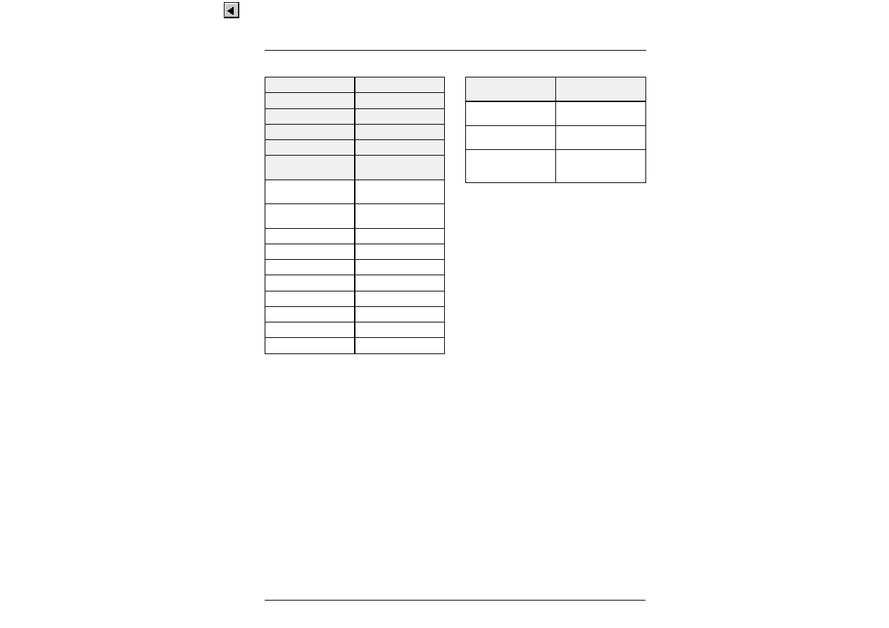
PRELIMINARY DATA SHEET
MSP 34x0D
Micronas
45
7.3.9. Channel Matrix Modes
The sum/difference mode can be used together with
the quasi-peak detector to determine the sound mate-
rial mode. If the difference signal on channel B (right)
is near to zero, and the sum signal on channel A (left)
is high, the incoming audio signal is mono. If there is a
significant level on the difference signal, the incoming
audio is stereo.
7.3.10. SCART Prescale
Loudspeaker Matrix
0008
hex
L
Headphone Matrix
0009
hex
L
SCART1 Matrix
000A
hex
L
SCART2 Matrix
0041
hex
L
I
2
S Matrix
000B
hex
L
Quasi-Peak
Detector Matrix
000C
hex
L
SOUNDA / LEFT /
MSP-IF-CHANNEL2
0000 0000
00
hex
RESET
SOUNDB / RIGHT /
MSP-IF-CHANNEL1
0001 0000
10
hex
STEREO
0010 0000
20
hex
MONO
0011 0000
30
hex
SUM / DIFF
0100 0000
40
hex
AB_XCHANGE
0101 0000
50
hex
PHASE_CHANGE_B
0110 0000
60
hex
PHASE_CHANGE_A
0111 0000
70
hex
A_ONLY
1000 0000
80
hex
B_ONLY
1001 0000
90
hex
Volume Prescale
SCART
000D
hex
H
OFF
0000 0000
00
hex
RESET
0 dB gain (2 V
RMS
input
to digital full scale)
0001 1001
19
hex
+14 dB gain
(400 mV
RMS
input to
digital full scale)
0111 1111
7F
hex
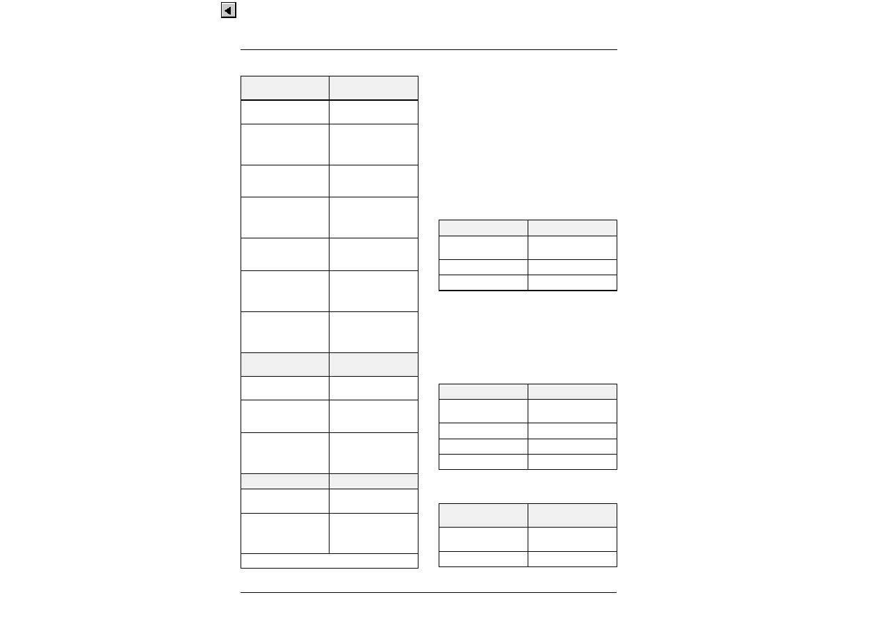
MSP 34x0D
PRELIMINARY DATA SHEET
46
Micronas
7.3.11. FM/AM Prescale
For the High Deviation Mode, the FM prescaling val-
ues can be used in the range from 14
hex
to 30
hex
.
Please consider the internal reduction of 6 dB for this
mode. The FIR-bandwidth should be selected to
500 kHz.
1)
Given deviations will result in internal digital full-
scale signals. Appropriate clipping headroom has to be
set by the customer. This can be done by decreasing
the listed values by a specific factor.
2)
In the mentioned SIF-level range, the AM-output
level remains stable and independent of the actual
SIF-level. In this case, only the AM degree of audio
signals above 40 Hz determines the AM-output level.
7.3.12. FM Matrix Modes (see also Table 4≠1)
NO_MATRIX is used for terrestrial mono or satellite
stereo sound. GSTEREO dematrixes [(L+R)/2, R] to
[L, R] and is used for German dual carrier stereo sys-
tem (Standard B/G). KSTEREO dematrixes [(L+R)/2,
(L
-
R)/2] to [L, R] and is used for the Korean dual car-
rier stereo system (Standard M).
7.3.13. FM Fixed Deemphasis
7.3.14. FM Adaptive Deemphasis
Volume Prescale FM
(Normal FM Mode)
000E
hex
H
OFF
0000 0000
00
hex
RESET
Maximum Volume
(28 kHz deviation
1)
recommended FIR-
bandwidth: 130 kHz)
0111 1111
7F
hex
Deviation 50 kHz
1)
recommended FIR-
bandwidth: 200 kHz
0100 1000
48
hex
Deviation 75 kHz
1)
recommended FIR-
bandwidth: 200 or
280 kHz
0011 0000
30
hex
Deviation 150 kHz
1)
recommended FIR-
bandwidth: 380 kHz
0001 1000
18
hex
Maximum deviation
192 kHz
1)
recommended FIR-
bandwidth: 380 kHz
0001 0011
13
hex
Prescale for adaptive
deemphasis WP1
recommended FIR-
bandwidth: 130 kHz
0001 0000
10
hex
Volume Prescale FM
(High Deviation Mode)
000E
hex
H
OFF
0000 0000
00
hex
RESET
Deviation 150 kHz
1)
recommended FIR-
bandwidth: 380 kHz
0011 0000
30
hex
Maximum deviation
384 kHz
1)
recommended FIR-
bandwidth: 500 kHz
0001 0100
14
hex
Volume Prescale AM
000E
hex
H
OFF
0000 0000
00
hex
RESET
SIF input level:
0.1 V
pp
-
0.8 V
pp
1)
2)
0.8 V
pp
-
1.4 V
pp
1)
0111 1100
7C
hex
<7C
hex
Note: For AM, the bit MODE_REG[15] must be 1
FM Matrix
000E
hex
L
NO MATRIX
0000 0000
00
hex
RESET
GSTEREO
0000 0001
01
hex
KSTEREO
0000 0010
02
hex
Deemphasis FM
000F
hex
H
50
µ
s
0000 0000
00
hex
RESET
75
µ
s
0000 0001
01
hex
J17
0000 0100
04
hex
OFF
0011 1111
3F
hex
FM Adaptive
Deemphasis WP1
000F
hex
L
OFF
0000 0000
00
hex
RESET
WP1
0011 1111
3F
hex

PRELIMINARY DATA SHEET
MSP 34x0D
Micronas
47
7.3.15. NICAM Prescale
7.3.16. NICAM Deemphasis
A J17 Deemphasis is always applied to the NICAM
signal. It is not switchable.
7.3.17. I
2
S1 and I
2
S2 Prescale
7.3.18. ACB Register
Definition of Digital Control Output Pins
Definition of SCART Switching Facilities
(see Fig. 4≠3 on page 13)
Note: If "MONO_IN" is selected at the DSP_IN selec-
tion, the channel matrix mode of the corresponding
output channel(s) must be set to "sound A".
Volume Prescale
NICAM
0010
hex
H
OFF
0000 0000
00
hex
RESET
0 dB gain
0010 0000
20
hex
+12 dB gain
0111 1111
7F
hex
Prescale I
2
S1
0016
hex
H
Prescale I
2
S2
0012
hex
H
OFF
0000 0000
00
hex
0 dB gain
0001 0000
10
hex
RESET
+18 dB gain
0111 1111
7F
hex
ACB Register
0013
hex
[15..14]
D_CTR_OUT0
low
(RESET)
high
x0
x1
D_CTR_OUT1
low
(RESET)
high
0x
1x
ACB Register
0013
hex
[13...0]
DSP IN
Selection of Source:
* SC1_IN_L/R
MONO_IN
SC2_IN_L/R
SC3_IN_L/R
SC4_IN_L/R
Mute
xx xx00 xx00 0000
xx xx01 xx00 0000
xx xx10 xx00 0000
xx xx11 xx00 0000
xx xx00 xx10 0000
xx xx11 xx10 0000
SC1_OUT_L/R
Selection of Source:
* SC3_IN_L/R
SC2_IN_L/R
MONO_IN
SCART1_L/R via D/A
SCART2_L/R via D/A
SC1_IN_L/R
SC4_IN_L/R
Mute
xx 00xx x0x0 0000
xx 01xx x0x0 0000
xx 10xx x0x0 0000
xx 11xx x0x0 0000
xx 00xx x1x0 0000
xx 01xx x1x0 0000
xx 10xx x1x0 0000
xx 11xx x1x0 0000
SC2_OUT_L/R
Selection of Source:
* SCART1_L/R via D/A
SC1_IN_L/R
MONO_IN
SCART2_L/R via D/A
SC2_IN_L/R
SC3_IN_L/R
SC4_IN_L/R
Mute
00 xxxx 0xx0 0000
01 xxxx 0xx0 0000
10 xxxx 0xx0 0000
00 xxxx 1xx0 0000
01 xxxx 1xx0 0000
10 xxxx 1xx0 0000
11 xxxx 1xx0 0000
11 xxxx 0xx0 0000
* = RESET position, which becomes active at the
time of the first write transmission on the control bus
to the audio processing part (DSP). By writing to the
ACB register first, the RESET state can be rede-
fined.
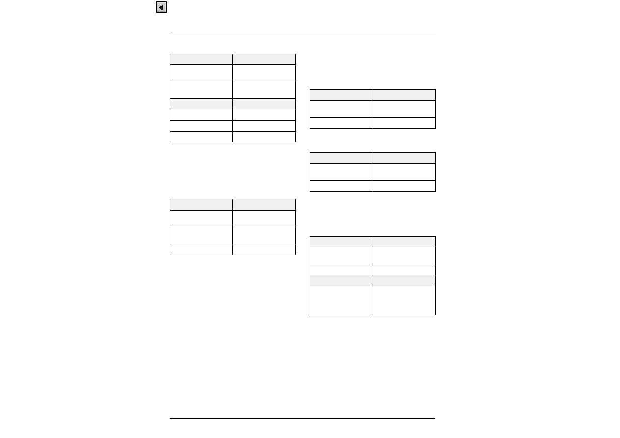
MSP 34x0D
PRELIMINARY DATA SHEET
48
Micronas
7.3.19. Beeper
A square wave beeper can be added to the loud-
speaker channel and the headphone channel. The
addition point is just before loudness and volume
adjustment.
7.3.20. Identification Mode
To shorten the response time of the identification algo-
rithm after a program change between two FM-Stereo
capable programs, the reset of the ident-filter can be
applied.
Sequence:
1. Program change
2. Reset ident-filter
3. Set identification mode back to standard B/G or M
4. Read stereo detection register
7.3.21. FM DC Notch
The DC compensation filter (FM DC Notch) for FM
input can be switched off. This is used to speed up the
automatic search function (see section 6.8.5. on page
35). In normal FM mode, the FM DC Notch should be
switched on.
7.3.22. Mode Tone Control
By means of `Mode Tone Control', Bass/Treble or
Equalizer may be activated.
7.3.23. Automatic Volume Correction (AVC)
Different sound sources (e.g. terrestrial channels, SAT
channels, or SCART) fairly often do not have the same
volume level. Advertisement during movies, as well,
usually has a different (higher) volume level than the
movie itself. The Automatic Volume Correction (AVC)
solves this problem and equalizes the volume levels.
Beeper Volume
0014
hex
H
OFF
0000 0000
00
hex
RESET
Maximum Volume (full
digital scale FDS)
0111 1111
7F
hex
Beeper Frequency
0014
hex
L
16 Hz (lowest)
0000 0001
01
hex
1 kHz
0100 0000
40
hex
4 kHz (highest)
1111 1111
FF
hex
Identification Mode
0015
hex
L
Standard B/G
(German Stereo)
0000 0000
00
hex
RESET
Standard M
(Korean Stereo)
0000 0001
01
hex
Reset of Ident-Filter
0011 1111
3F
hex
FM DC Notch
0017
hex
L
ON
0000 0000
00
hex
Reset
OFF
0011 1111
3F
hex
Mode Tone Control
0020
hex
H
Bass and Treble
0000 0000
00
hex
RESET
Equalizer
1111 1111
FF
hex
AVC
On/Off
0029
hex
[15...12]
AVC
off and Reset
of int. variables
0000
0
hex
RESET
AVC
on
1000
8
hex
AVC
Decay Time
0029
hex
[11...8]
8 sec. (long)
4 sec. (middle)
2 sec. (short)
20 ms (very short)
1000
8
hex
0100
4
hex
0010
2
hex
0001
1
hex
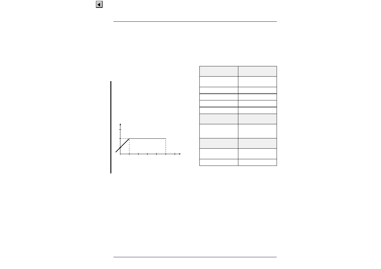
PRELIMINARY DATA SHEET
MSP 34x0D
Micronas
49
The absolute value of the incoming signal is fed into a
filter with 16 ms attack time and selectable decay time.
The decay time must be adjusted as shown in the
table above. This attack/decay filter block works simi-
lar to a peak hold function. The volume correction
value with its quasi continuous step width is calculated
using the attack/decay filter output.
The Automatic Volume Correction functions with an
internal reference level of
-
18 dBr. This means that
input signals with a volume level of
-
18 dBr will not be
affected by the AVC. If the input signals vary in a range
of
-
24 dB to 0 dB, the AVC maintains a fixed output
level of
-
18 dBr.
Fig. 7≠1 shows the AVC output level versus its input
level. For prescale and volume registers set to 0 dB, a
level of 0 dBr corresponds to full scale input / output.
This is
≠ SCART in-, output 0 dBr
=
2.0 V
rms
≠ Loudspeaker and Aux output 0 dBr
=
1.4 V
rms
Fig. 7≠1: Simplified AVC characteristics
To reset the internal variables, the AVC should be
switched off and on during any channel or source
change. For standard applications, the recommended
decay time is 4 sec.
Note: AVC should not be used in any Dolby Pro Logic
mode, except PANORAMA, where no other than the
loudspeaker output is active.
7.3.24. Subwoofer Channel
The subwoofer channel is created by combining the left
and right channels directly behind the tone control filter
block. A third order low-pass filter with programmable
corner frequency and volume adjustment according to
the main channel output is performed to the bass sig-
nal. Additionally, at the loudspeaker channels, a com-
plementary high-pass filter can be switched on.
-
30
-
24
-
18
-
12
-
6
+
6
input level
-
18
-
24
-
12
output level
0
[dBr]
[dBr]
Subwoofer Channel
Volume Adjust
002C
hex
H
0 dB
0000 0000
00
hex
RESET
-
1 dB
1111 1111
FF
hex
-
29 dB
1110 0011
E3
hex
-
30 dB
1110 0010
E2
hex
Mute
1000 0000
80
hex
Subwoofer Channel
Corner Frequency
002D
hex
H
50 Hz ... 400 Hz
e.g. 50 Hz = 5
dec
400 Hz = 40
dec
RESET
00
hex
0000 0101
05
hex
0010 1000
28
hex
Subwoofer: Comple-
mentary High-pass
002D
hex
L
HP off
0000 0000
00
hex
RESET
HP on
0000 0001
01
hex
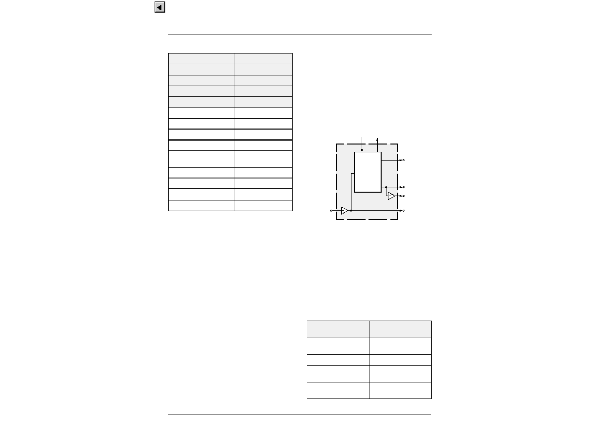
MSP 34x0D
PRELIMINARY DATA SHEET
50
Micronas
7.3.25. Equalizer Loudspeaker Channel
With positive equalizer settings, internal overflow may
occur even with overall volume less than 0 dB. This
will lead to a clipped output signal. Therefore, it is not
recommended to set equalizer bands to a value that, in
conjunction with volume, would result in an overall
positive gain.
Equalizer must not be used simultaneously with Bass
and Treble (Mode Tone Control must be set to FF to
use the Equalizer). If Bass and Treble are used, Equal-
izer coefficients must be set to zero.
7.4. Exclusions for the Audio Baseband Features
In general, all functions can be switched independently
of the others. Exceptions:
1. NICAM cannot be processed simultaneously with
the FM2 channel.
2. FM adaptive deemphasis WPI cannot be processed
simultaneously with the FM-identification.
7.5. Phase Relationship of Analog Outputs
The analog output signals: Loudspeaker, headphone,
and SCART2 all have the same phases. The user
does not need to change output phases when using
these analog outputs directly. The SCART1 output has
opposite phase.
Using the I
2
S-outputs for other DSPs or D/A convert-
ers, care must be taken to adjust for the correct phase.
If the attached coprocessor is one of the MSP family,
the following schematics help to determine the phase
relationship.
Fig. 7≠2: Phase diagram of the MSP 34x0D
7.6. DSP Read Registers: Functions and Values
All readable registers are 16-bit wide. Transmissions
via I
2
C bus have to take place in 16-bit words. Single
data entries are 8 bit. Some of the defined 16-bit words
are divided into low and high byte, thus holding two dif-
ferent control entities.
These registers are not writable.
7.6.1. Stereo Detection Register
Band 1 (below 120 Hz)
0021
hex
H
Band 2 (Center: 500 Hz)
0022
hex
H
Band 3 (Center: 1.5 kHz)
0023
hex
H
Band 4 (Center: 5 kHz)
0024
hex
H
Band 5 (above 10 kHz)
0025
hex
H
+12 dB
0110 0000
60
hex
+11 dB
0101 1000
58
hex
+1 dB
0000 1000
08
hex
+1/8 dB
0000 0001
01
hex
0 dB
0000 0000
00
hex
RESET
-
1/8 dB
1111 1111
FF
hex
-
1 dB
1111 1000
F8
hex
-
11dB
1010 1000
A8
hex
-
12 dB
1010 0000
A0
hex
Stereo Detection
Register
0018
hex
H
Stereo Mode
Reading
(two's complement)
MONO
near zero
STEREO
positive value (ideal
reception: 7F
hex
)
BILINGUAL
negative value (ideal
reception: 80
hex)
Audio
Baseband
Processing
SCART1
Mono
SCART1...3
I2S_in I2S_out
SCART2
Loudspeaker
Headphone
SCART1...2
PRELIMINARY DATA SHEET
MSP 34x0D
Micronas
51
7.6.2. Quasi-Peak Detector
The quasi peak readout register can be used to read
out the quasi peak level of any input source, in order to
adjust all inputs to the same normal listening level. The
refresh rate is 32 kHz. The feature is based on the fil-
ter time constants:
attack time: 1.3 ms
decay time: 37 ms
7.6.3. DC Level Register
The DC level register measures the DC component of
the incoming FM signals (FM1 and FM2). This can be
used for seek functions in satellite receivers and for IF
FM frequencies fine tuning. A too low demodulation
frequency (DCO) results in a positive DC-level and
vice-versa. For further processing, the DC content of
the demodulated FM signals is suppressed. The time
constant
,
defining the transition time of the DC Level
Register, is approximately 28 ms.
7.6.4. MSP Hardware Version Code
A change in the hardware version code defines hard-
ware optimizations that may have influence on the
chip's behavior. The readout of this register is identical
to the hardware version code in the chip's imprint.
7.6.5. MSP Major Revision Code
The MSP 34x0D is the fourth generation of ICs in the
MSP family.
7.6.6. MSP Product Code
By means of the MSP product code, the control pro-
cessor is able to decide whether or not NICAM-control-
ling should be accomplished.
7.6.7. MSP ROM Version Code
A change in the ROM version code defines internal
software optimizations, that may have influence on the
chip's behavior, e.g. new features may have been
included. While a software change is intended to cre-
ate no compatibility problems, customers that would
like to use the new functions, can identify new
MSP 34x0D versions according to this number. To
avoid compatibility problems with MSP 34x0B, an off-
set of 20
hex
is added to the ROM version code of the
chip's imprint.
Quasi-Peak
Readout Left
0019
hex
H+L
Quasi-Peak
Readout Right
001A
hex
H+L
Quasi peak readout
[0000
hex
... 7FFF
hex
]
values are 16 bit two's
complement
DC Level Readout
FM1 (MSP-Ch2)
001B
hex
H+L
DC Level Readout
FM2 (MSP-Ch1)
001C
hex
H+L
DC Level
[8000
hex
... 7FFF
hex
]
values are 16 bit two's
complement
Hardware Version
001E
hex
H
Hardware Version
[00
hex
... FF
hex
]
MSP 34x0D
-
B4
02
hex
Major Revision
001E
hex
L
MSP 34x0D
04
hex
Product
001F
hex
H
MSP 3400D
0000 0000
00
hex
MSP 3410D
0000 1010
0A
hex
ROM Version
001F
hex
L
Major software revision
[00
hex
... FF
hex
]
MSP 34x0D
-
B4
0010 0100
24
hex
MSP 34x0D
PRELIMINARY DATA SHEET
52
Micronas
8. Differences between MSP 3400C, MSP 3400D, MSP 3410B, and MSP 3410D
Feature
MSP 3400C
MSP 3400D
-
B4
MSP 3410B
-
F7
MSP 3410D
-
B4
Hardware
NICAM
No
No
Yes
Yes
S-Bus Output
No
No
S_DA_OUT
No
S-Bus Input
S_DA_IN
No
S_DA_IN
No
Second I
2
S Data Input
I2S_DA_IN2
I2S_DA_IN2
No
I2S_DA_IN2
ADR Interface
ADR_CL,
ADR_WS,
ADR_DA
ADR_CL,
ADR_WS,
ADR_DA
No
ADR_CL,
ADR_WS,
ADR_DA
Second SCART D/A Converter
No
Yes
No
Yes
Demodulator
Demodulator Short Programming
No
Yes
No
Yes
Autodetection for terr. TV Sound Standards
No
Yes
No
Yes
Automatic switching from NICAM to FM and vv.
No
Yes
No
Yes
ADCV[10]
Carrier Mute Level
Carrier Mute
Level
not used
FIFO Watchdog
On/Off
not used
ADCV[11]
Carrier Mute Level
Carrier Mute
Level
not used
not used
not used
MODE_REG[1]:
Tri-state digital outputs
0: active
1: tri-state
0: active
1: tri-state
enable Pay-TV
0: active
1: tri-state
MODE_REG[2]:
Tri-state digital outputs
I
2
S outputs
0: active
1: tri-state
0: active
1: tri-state
disable NICAM
Descrambler
0: active
1: tri-state
MODE_REG[6]:
NICAM
no function
no function
0: FM
1: NICAM
0: FM
1: NICAM
MODE_REG[7]:
FM1FM2
no function
no function
0: NICAM
1: FM
no function
MODE_REG[10]:
S-Bus Setting
no function
no function
NICAM/FM on
S-Bus
no function
MODE_REG[11]:
S-Bus Mode
no function
no function
Mode of internal
S-Bus
no function
MODE_REG[12]:
6 dB gain in
MSP-Ch1
0: on
1: off
0: on
1: off
always on
0: on
1: off
MODE_REG[13]:
FIR filter coeff. set for
MSP-Ch1
0: use FIR1
1: use FIR2
0: use FIR1
1: use FIR2
always FIR1
0: use FIR1
1: use FIR2
MODE_REG[14]
Mode of ADR Interface
0: normal mode
1: ADR/SaRa
0: normal mode
1: ADR/SaRa
No
0: normal mode
1: ADR/SaRa

PRELIMINARY DATA SHEET
MSP 34x0D
Micronas
53
Demodulator
MODE_REG[15]:
Gain for AM-Demodulation
0: 0 dB
1)
1: 12 dB
0: 0 dB
1: 12 dB
No
0: 0 dB
1: 12 dB
FAWCT_SOLL
(DEMOD W Addr. 107
hex
)
Not necessary
Not necessary
Yes
Not necessary
FAWCT_ER_TOL
(DEMOD W Addr. 10F
hex
)
Not necessary
Not necessary
Yes
Not necessary
AUDIO_PLL
(DEMOD W Addr. 2D7
hex
)
Not necessary
Not necessary
Yes
Not necessary
LOAD_REG_1/2
(DEMOD W Addr. 56
hex
)
Not necessary
Not necessary
Yes
Not necessary
LOAD_REG_1
(DEMOD W Addr. 60
hex
)
Not necessary
Not necessary
Yes
Not necessary
SEARCH_NICAM (DEMOD W Addr. 78
hex
)
No
Not necessary
Yes
Not necessary
SELF_TEST
(DEMOD W Addr. 792
hex
)
No
not compatible,
not for customer
use,
values as
described in
Mubi-Software
not compatible,
not for customer
use,
FAWCT_IST
(DEMOD R Addr.
25
hex
)
No
No
Yes
Yes, but not
necessary
CONC_CT
(DEMOD R Addr. 58
hex
)
No
No
Yes
Yes, but not
recommended
ERROR_RATE
(DEMOD R Addr. 57
hex
)
No
No
No
Yes
Reading out RMS value of AGC
I
2
C Addr.
001E
hex
I
2
C Addr.
021E
hex
not possible
I
2
C Addr.
021E
hex
Reading out internal PLL capacitance switches
I
2
C Addr.
001F
hex
I
2
C Addr.
021F
hex
not possible
I
2
C Addr.
021F
hex
Audio Baseband Processing
Improved oversampling filters for all
D/A converters
Yes
Yes
No
Yes
Mode Loudness Loudspeaker channel
(DSP W Addr. 0004
hex
L)
00
hex
: normal
04
hex
: Super
Bass
00
hex
: normal
04
hex
: Super
Bass
00
hex
: normal
04
hex
: Super
Version
F7
00
hex
: normal
04
hex
: Super
Bass
Spatial Effect Loudspeaker
(DSP W Addr. 05
hex
L)
Mode/
Customize
Mode/
Customize
always 0
Mode/
Customize
Prescale I
2
S2
(DSP W Addr. 0012
hex
H)
Yes
1)
Yes
No
Yes
Prescale I
2
S1
(DSP W Addr. 0016
hex
H)
Yes
1)
Yes
No
Yes
FM DC Notch switchable
(DSP W Addr. 0017
hex
)
Yes
Yes
No
Yes
Mode Tone Control Loudspeaker channel
(DSP W Addr. 0020
hex
H)
00
hex
: Bass/
Treble
FF
hex
:Equalizer
00
hex
: Bass/
Treble
FF
hex
:Equalizer
always Bass/
Treble
00
hex
: Bass/
Treble
FF
hex
:Equalizer
5 Band Equalizer
(DSP W Addr.
0021
hex
-
0025
hex
)
[+12 ...
-
12 dB]
[+12 ...
-
12 dB]
not implemented
[+12 ...
-
12 dB]
Balance Headphone channel
(DSP W Addr. 0030
hex
H)
Yes
1)
Yes
No
Yes
1)
This feature will be implemented in MSP 3400C from version C7 on.
Feature
MSP 3400C
MSP 3400D
-
B4
MSP 3410B
-
F7
MSP 3410D
-
B4

MSP 34x0D
PRELIMINARY DATA SHEET
54
Micronas
Audio Baseband Processing
Bass for Loudspeaker and Headphone chan.
(DSP W Addr. 0002/0031
hex
H)
Yes
1)
[+20 ...
-
12 dB]
Yes
[+20 ...
-
12 dB]
No
Yes
[+20 ...
-
12 dB]
Treble for Loudspeaker and Headphone chan.
(DSP W Addr. 0003/0032
hex
H)
Yes
1)
[+15 ...
-
12 dB]
Yes
[+15 ...
-
12 dB]
No
Yes
[+15 ...
-
12 dB]
Loudness Headphone channel
(DSP W Addr. 0033
hex
H)
Yes
1)
Yes
No
Yes
Mode Loudness Headphone channel
(DSP W Addr. 0033
hex
L)
00
hex
: normal
04
hex
: Super
Bass
1)
00
hex
: normal
04
hex
: Super
Bass
No
00
hex
: normal
04
hex
: Super
Bass
SCART1/2 Volume in dB
(DSP W Addr. 0007/0040
hex
H)
Yes
1)
(SCART1)
Yes
No
Yes
Scart 2 Volume (DSP W Addr. 0040
hex
H)
No
Yes
No
Yes
Scart 2 Source (DSP W Addr. 0041
hex
H)
No
Yes
No
Yes
Scart 2 Matrix
(DSP W Addr. 0041
hex
L)
No
Yes
No
Yes
Full SCART I/O Matrix without restrictions
No
Yes
No
Yes
Balance of loudspeaker and headphone
channels in dB units
(DSP W Addr. 0016/0012
hex
)
Yes
1)
Yes
No
Yes
Subwoofer output
No
Yes
No
Yes
Automatic Volume Correction (AVC)
No
Yes
No
Yes
1)
This feature will be implemented in MSP 3400C from version C7 on.
Feature
MSP 3400C
MSP 3400D
-
B4
MSP 3410B
-
F7
MSP 3410D
-
B4

PRELIMINARY DATA SHEET
MSP 34x0D
Micronas
55
9. Specifications
9.1. Outline Dimensions
Fig. 9≠1:
68-Pin Plastic Leaded Chip Carrier Package
(PLCC68)
Weight approximately 4.8 g
Dimensions in mm
Fig. 9≠2:
64-Pin Plastic Shrink Dual Inline Package
(PSDIP64)
Weight approximately 9.0 g
Dimensions in mm
Fig. 9≠3:
52-Pin Plastic Shrink Dual Inline Package
(PSDIP52)
Weight approximately 5.5 g
Dimensions in mm
x 45
∞
1.1
25.125
0.125
±
0.22
0.07
±
1.2 x 45
∞
16 x 1.27
= 20.32
0.1
±
0.1
±
24.22
0.1
±
2
43
27
26
10
9
61
9
44
60
1
0.48
0.71
1
1.9
4.05
0.1
4.75
±
0.15
1.27
0.1
±
2
15
9
1.27
0.1
±
16 x 1.27
= 20.32
0.1
±
0.1
±
24.22
0.1
±
0.9
23.4
SPGS7004-3/5E
25.125
0.125
±
1.6
0.457
1.29
1
32
33
64
3
0.3
1.9
(1)
1.778
±
0.05
1
±
0.1
57.7
±
0.1
3.2
±
0.4
3.8
±
0.1
4.8
±
0.4
19.3
±
0.1
18
±
0.1
20.1
±
0.5
0.27
±
0.06
SPGS0016-4/3E
31 x 1.778 = 55.118
±
0.1
2.5
0.3
0.24
0.3
14
±
0.1
1.778
±
0.05
1
26
27
52
0.457
0
∞
...15
∞
47
±
0.1
0.4
±
0.2
4
±
0.1
3.2
±
0.2
1
±
0.1
15.6
±
0.1
0.27
±
0.06
25 x 1.778 = 44.47
±
0.1
SPGS0015-1/2E

MSP 34x0D
PRELIMINARY DATA SHEET
56
Micronas
Fig. 9≠4:
80-Pin Plastic Quad Flat Pack
(PQFP80)
Weight approximately 1.61 g
Dimensions in mm
Fig. 9≠5:
64-Pin Plastic Low-Profile Quad Flat Pack
(PLQFP64)
Weight approximately 0.35 g
Dimensions in mm
17.2
23.2
8
9.8
1.8
14
20
16
5
8
10.3
23 x 0.8 = 18.4
15 x 0.8 = 12.0
0.8
0.8
41
64
24
1
65
80
40
25
1.28
2.70
1.8
0.1
3
±
0.2
0.17
±
0.03
SPGS0025-1/1E
1.75
1.75
49
64
1
16
17
32
33
48
12
12
D0025/2E
0.5
10
10
0.5
15 x 0.5 = 7.5
15 x 0.5 = 7.5
1.5
1.4
0.145
0.1
0.22

PRELIMINARY DATA SHEET
MSP 34x0D
Micronas
57
9.2. Pin Connections and Short Descriptions
NC = not connected (leave vacant for future compatibility reasons)
TP = Test Pin (leave vacant; pin is used for production test only)
LV = leave vacant
X = obligatory; connect as described in application circuit diagram
Pin No.
Pin Name
Type
Connection
Short Description
PLCC
68-pin
PSDIP
64-pin
PSDIP
52-pin
PQFP
80-pin
PLQFP
64-pin
(if not used)
1
16
14
9
8
ADR_WS
OUT
LV
ADR word strobe
2
-
-
-
-
NC
LV
Not connected
3
15
13
8
7
ADR_DA
OUT
LV
ADR data output
4
14
12
7
6
I2S_DA_IN1
IN
LV
I
2
S1 data input
5
13
11
6
5
I2S_DA_OUT
OUT
LV
I
2
S data output
6
12
10
5
4
I2S_WS
IN/OUT
LV
I
2
S word strobe
7
11
9
4
3
I2S_CL
IN/OUT
LV
I
2
S clock
8
10
8
3
2
I2C_DA
IN/OUT
X
I
2
C data
9
9
7
2
1
I2C_CL
IN/OUT
X
I
2
C clock
10
8
-
1
64
NC
LV
Not connected
11
7
6
80
63
STANDBYQ
IN
X
Standby (low-active)
12
6
5
79
62
ADR_SEL
IN
X
I
2
C Bus address select
13
5
4
78
61
D_CTR_OUT0
OUT
LV
Digital control output 0
14
4
3
77
60
D_CTR_OUT1
OUT
LV
Digital control output 1
15
3
-
76
59
NC
LV
Not connected
16
2
-
75
58
NC
LV
Not connected
17
-
-
-
-
NC
LV
Not connected
18
1
2
74
57
AUD_CL_OUT
OUT
LV
Audio clock output
(18.432 MHz)
19
64
1
73
56
TP
LV
Test pin
20
63
52
72
55
XTAL_OUT
OUT
X
Crystal oscillator
21
62
51
71
54
XTAL_IN
IN
X
Crystal oscillator
22
61
50
70
53
TESTEN
IN
X
Test pin
23
60
49
69
52
ANA_IN2+
IN
AVSS via
56 pF / LV
IF input 2
(can be left vacant only if
IF input1 is also not in use)
24
59
48
68
51
ANA_IN
-
IN
AVSS via
56 pF / LV
IF common
(can be left vacant only if
IF input1 is also not in use)
25
58
47
67
50
ANA_IN1+
IN
LV
IF input 1
MSP 34x0D
PRELIMINARY DATA SHEET
58
Micronas
26
57
46
66
49
AVSUP
X
Analog power supply 5V
-
-
-
65
-
AVSUP
X
Analog power supply 5V
-
-
-
64
-
NC
LV
Not connected
-
-
-
63
-
NC
LV
Not connected
27
56
45
62
48
AVSS
X
Analog ground
-
-
-
61
-
AVSS
X
Analog ground
28
55
44
60
47
MONO_IN
IN
LV
Mono input
-
-
-
59
-
NC
LV
Not connected
29
54
43
58
46
VREFTOP
X
Reference voltage
IF A/D converter
30
53
42
57
45
SC1_IN_R
IN
LV
SCART 1 input, right
31
52
41
56
44
SC1_IN_L
IN
LV
SCART 1 input, left
32
51
-
55
43
ASG1
AHVSS
Analog Shield Ground 1
33
50
40
54
42
SC2_IN_R
IN
LV
SCART 2 input, right
34
49
39
53
41
SC2_IN_L
IN
LV
SCART 2 input, left
35
48
-
52
40
ASG2
AHVSS
Analog Shield Ground 2
36
47
38
51
39
SC3_IN_R
IN
LV
SCART 3 input, right
37
46
37
50
38
SC3_IN_L
IN
LV
SCART 3 input, left
38
45
-
49
37
ASG4
AHVSS
Analog Shield Ground 4
39
44
-
48
36
SC4_IN_R
IN
LV
SCART 4 input, right
40
43
-
47
35
SC4_IN_L
IN
LV
SCART 4 input, left
41
-
-
46
-
NC
LV or AHVSS
Not connected
42
42
36
45
34
AGNDC
X
Analog reference
voltage
43
41
35
44
33
AHVSS
X
Analog ground
-
-
-
43
-
AHVSS
X
Analog ground
-
-
-
42
-
NC
LV
Not connected
-
-
-
41
-
NC
LV
Not connected
44
40
34
40
32
CAPL_M
X
Volume capacitor MAIN
45
39
33
39
31
AHVSUP
X
Analog power supply 8V
46
38
32
38
30
CAPL_A
X
Volume capacitor AUX
47
37
31
37
29
SC1_OUT_L
OUT
LV
SCART 1 output, left
Pin No.
Pin Name
Type
Connection
Short Description
PLCC
68-pin
PSDIP
64-pin
PSDIP
52-pin
PQFP
80-pin
PLQFP
64-pin
(if not used)

PRELIMINARY DATA SHEET
MSP 34x0D
Micronas
59
48
36
30
36
28
SC1_OUT_R
OUT
LV
SCART 1 output, right
49
35
29
35
27
VREF1
X
Reference ground 1
high voltage part
50
34
28
34
26
SC2_OUT_L
OUT
LV
SCART 2 output, left
51
33
27
33
25
SC2_OUT_R
OUT
LV
SCART 2 output, right
52
-
-
32
-
NC
LV
1)
Not connected
53
32
-
31
24
NC
LV
Not connected
54
31
26
30
23
DACM_SUB
LV
Subwoofer output
55
30
-
29
22
NC
LV
Not connected
56
29
25
28
21
DACM_L
OUT
LV
Loudspeaker out, left
57
28
24
27
20
DACM_R
OUT
LV
Loudspeaker out, right
58
27
23
26
19
VREF2
X
Reference ground 2
59
26
22
25
18
DACA_L
OUT
LV
Headphone out, left
60
25
21
24
17
DACA_R
OUT
LV
Headphone out, right
-
-
-
23
-
NC
LV
Not connected
-
-
-
22
-
NC
LV
Not connected
61
24
20
21
16
RESETQ
IN
X
Power-on reset
62
23
-
20
15
NC
LV
Not connected
63
22
-
19
14
NC
LV
Not connected
64
21
19
18
13
NC
LV
Not connected
65
20
18
17
12
I2S_DA_IN2
IN
LV
I
2
S2 data input
66
19
17
16
11
DVSS
X
Digital ground
-
-
-
15
-
DVSS
X
Digital ground
-
-
-
14
-
DVSS
X
Digital ground
67
18
16
13
10
DVSUP
X
Digital power supply 5V
-
-
-
12
-
DVSUP
X
Digital power supply 5V
-
-
-
11
-
DVSUP
X
Digital power supply 5V
68
17
15
10
9
ADR_CL
OUT
LV
ADR clock
1)
Due to compatibility with MSP 3410D-B4 and older versions, it is possible to connect with ground as well.
Pin No.
Pin Name
Type
Connection
Short Description
PLCC
68-pin
PSDIP
64-pin
PSDIP
52-pin
PQFP
80-pin
PLQFP
64-pin
(if not used)

MSP 34x0D
PRELIMINARY DATA SHEET
60
Micronas
9.3. Pin Configurations
Fig. 9≠6: 68-pin PLCC package
10
11
12
13
14
15
16
17
18
19
20
21
22
23
24
25
60
59
58
57
56
55
54
53
52
51
50
49
48
47
46
45
27 28 29 30 31 32 33 34 35 36 37 38 39 40 41 42 43
9
8
7
6
5
4
3
2
1
68 67 66 65 64 63 62 61
26
44
MSP 34x0D
NC
STANDBYQ
ADR_SEL
D_CTR_OUT0
D_CTR_OUT1
NC
NC
NC
AUD_CL_OUT
TP
XTAL_OUT
XTAL_IN
TESTEN
ANA_IN2+
ANA_IN
-
ANA_IN1+
DACA_R
DACA_L
VREF2
DACM_R
DACM_L
NC
DACM_SUB
NC
NC
SC2_OUT_R
SC2_OUT_L
VREF1
SC1_OUT_R
SC1_OUT_L
CAPL_A
AHVSUP
I2C_DA
I2S_CL
I2S_WS
I2S_DA_OUT
I2S_DA_IN1
ADR_DA
NC
ADR_WS
I2C_CL
ADR_CL
DVSUP
DVSS
I2S_DA_IN2
NC
NC
NC
RESETQ
MONO_IN
VREFTOP
SC1_IN_R
SC1_IN_L
ASG1
SC2_IN_R
SC2_IN_L
AVSS
SC3_IN_R
SC3_IN_L
ASG4
SC4_IN_R
SC4_IN_L
NC
AGNDC
AHVSS
ASG2
AVSUP
CAPL_M

PRELIMINARY DATA SHEET
MSP 34x0D
Micronas
61
Fig. 9≠7: 64-pin PSDIP package
Fig. 9≠8: 52-pin PSDIP package
1
AUD_CL_OUT
2
NC
3
NC
4
D_CTR_OUT1
5
D_CTR_OUT0
6
ADR_SEL
7
STANDBYQ
8
NC
9
I2C_CL
10
I2C_DA
11
I2S_CL
12
I2S_WS
13
I2S_DA_OUT
14
I2S_DA_IN1
15
ADR_DA
16
ADR_WS
TP
64
XTAL_OUT
63
XTAL_IN
62
TESTEN
61
ANA_IN2+
60
ANA_IN
-
59
ANA_IN+
58
AVSUP
57
AVSS
56
MONO_IN
55
VREFTOP
54
SC1_IN_R
53
SC1_IN_L
52
ASG1
51
SC2_IN_R
50
SC2_IN_L
49
17
ADR_CL
18
DVSUP
19
DVSS
20
I2S_DA_IN2
21
NC
22
NC
23
NC
24
RESETQ
25
DACA_R
26
DACA_L
ASG2
48
SC3_IN_R
47
SC3_IN_L
46
ASG4
45
SC4_IN_R
44
SC4_IN_L
43
AGNDC
42
AHVSS
41
CAPL_M
40
AHVSUP
39
MS
P
34
x0
D
VREF2
DACM_R
DACM_L
NC
DACM_SUB
NC
38
37
36
35
34
33
27
28
29
30
31
32
CAPL_A
SC1_OUT_L
SC1_OUT_R
VREF1
SC2_OUT_L
SC2_OUT_R
1
2
3
4
5
6
7
8
9
10
11
12
13
14
15
16
17
18
19
20
21
22
23
24
25
26
52
51
50
49
48
47
46
45
44
43
42
41
40
39
38
37
36
35
34
33
32
31
30
29
28
27
TP
AUD_CL_OUT
D_CTR_OUT1
D_CTR_OUT0
ADR_SEL
STANDBYQ
I2C_CL
I2C_DA
I2S_CL
I2S_WS
I2S_DA_OUT
I2S_DA_IN1
ADR_DA
ADR_WS
ADR_CL
DVSUP
XTAL_OUT
XTAL_IN
TESTEN
ANA_IN2+
ANA_IN
-
ANA_IN1+
AVSUP
AVSS
MONO_IN
VREFTOP
SC1_IN_R
SC1_IN_L
SC2_IN_R
SC2_IN_L
SC3_IN_R
SC3_IN_L
DVSS
I2S_DA_IN2
NC
RESETQ
DACA_R
DACA_L
VREF2
DACM_R
DACM_L
DACM_SUB
AGNDC
AHVSS
CAPL_M
AHVSUP
CAPL_A
SC1_OUT_L
SC1_OUT_R
VREF1
SC2_OUT_L
SC2_OUT_R
M
S
P
34
x0
D

MSP 34x0D
PRELIMINARY DATA SHEET
62
Micronas
Fig. 9≠9: 80-pin PQFP package
65
66
67
68
69
70
71
72
73
74
75
76
77
78
79
80
40
39
38
37
36
35
34
33
32
31
30
29
28
27
26
25
1
2
3
4
5
6
7
8
9
10 11 12 13 14 15 16 17 18 19 20 21 22 23 24
64 63 62 61 60 59 58 57 56 55 54 53 52 51 50 49 48 47 46 45 44 43 42 41
AVSUP
AVSUP
ANA_IN1+
ANA_IN
-
ANA_IN2+
TESTEN
XTAL_IN
XTAL_OUT
TP
AUD_CL_OUT
NC
NC
D_CTR_OUT1
D_CTR_OUT0
ADR_SEL
STANDBYQ
CAPL_M
AHVSUP
CAPL_A
SC1_OUT_L
SC1_OUT_R
VREF1
SC2_OUT_L
SC2_OUT_R
ASG3
NC
DACM_SUB
NC
DACM_L
DACM_R
VREF2
DACA_L
NC
AVSS
AVSS
MONO_IN
NC
VREFTOP
SC1_IN_R
SC1_IN_L
ASG1
NC
SC2_IN_R
SC2_IN_L
ASG2
SC3_IN_R
SC3_IN_L
ASG4
SC4_IN_R
SC4_IN_L
NC
AGNDC
AHVSS
AHVSS
NC
NC
I2C_CL
I2C_DA
I2S_CL
I2S_WS
I2S_DA_OUT
I2S_DA_IN1
ADR_DA
ADR_WS
ADR_CL
NC
DVSUP
DVSUP
DVSUP
DVSS
DVSS
DVSS
I2S_DA_IN2
NC
NC
NC
RESETQ
NC
NC
DACA_R
MSP 34x0D

PRELIMINARY DATA SHEET
MSP 34x0D
Micronas
63
Fig. 9≠10: 64-pin PLQFP package
AVSUP
ANA_IN1+
ANA_IN-
ANA_IN2+
TESTEN
XTAL_IN
XTAL_OUT
TP
AUD_CL_OUT
NC
NC
D_CTR_OUT1
D_CTR_OUT0
ADR_SEL
STANDBYQ
NC
CAPL_M
AHVSUP
CAPL_A
SC1_OUT_L
SC1_OUT_R
VREF1
SC2_OUT_L
SC2_OUT_R
NC
DACM_SUB
NC
DACM_L
DACM_R
VREF2
DACA_L
DACA_R
MONO_IN
VREFTOP
SC1_IN_R
SC1_IN_L
ASG1
SC2_IN_R
SC2_IN_L
AVSS
ASG2
SC3_IN_R
SC3_IN_L
ASG4
SC4_IN_R
SC4_IN_L
AGNDC
AHVSS
I2C_DA
I2S_CL
I2S_WS
I2S_DA_OUT
I2S_DA_IN1
ADR_DA
ADR_WS
I2C_CL
ADR_CL
DVSUP
DVSS
I2S_DA_IN2
NC
NC
NC
RESETQ
MSP 34x0D
49
50
51
52
53
54
55
56
57
58
59
60
61
62
63
64
32
31
30
29
28
27
26
25
24
23
22
21
20
19
18
17
1
2
3
4
5
6
7
8
9
10 11 12 13 14 15 16
48 47 46 45 44 43 42 41 40 39 38 37 36 35 34 33

MSP 34x0D
PRELIMINARY DATA SHEET
64
Micronas
9.4. Pin Circuits (pin numbers refer to PLCC68 package)
Fig. 9≠11: Output Pins 1, 3, 5, 13, 14, and 68
(ADR_WS, ADR_CL, ADR_DA, I2S_DA_OUT,
D_CTR_OUT0/1)
Fig. 9≠12: Input/Output Pins 8 and 9
(I2C_DA, I2C_CL)
Fig. 9≠13: Input Pins 4, 11, 12, 61, 62, and 65
(STANDBYQ, ADR_SEL, RESETQ, TESTEN,
I2S_DA_IN1, I2S_DA_IN2)
Fig. 9≠14: Input/Output Pins 6 and 7
(I2S_WS, I2S_CL)
Fig. 9≠15: Output/Input Pins 18, 20, and 21
(AUD_CL_OUT, XTALIN/OUT)
Fig. 9≠16: Input Pins 23-25, and 29
(ANA_IN2+, ANA_IN-, ANA_IN1+, VREFTOP)
Fig. 9≠17: Capacitor Pins 44 and 46
(CAPL_M, CAPL_A)
Fig. 9≠18: Input Pin 28 (MONO_IN)
DVSUP
P
N
GND
N
GND
DVSUP
P
N
GND
3
-
30 pF
2.5 V
500 k
3
-
30 pF
P
N
D
A
ANAIN1+
VREFTOP
ANAIN
-
ANAIN2+
0...2 V
3.75 V
24 k

PRELIMINARY DATA SHEET
MSP 34x0D
Micronas
65
Fig. 9≠19: Input Pins 30, 31, 33, 34, 36, 37, 40, and 41
(SC1-4_IN_L/R)
Fig. 9≠20: Output Pins 56, 57, 59, 60, and 54
(DACA_L/R, DACM_L/R, DACM_SUB)
Fig. 9≠21: Pin 42 (AGNDC)
Fig. 9≠22: Output Pins 47, 48, 50, and 51
(SC_1/2_OUT_L/R)
3.75 V
40 k
AHVSUP
0...1.2 mA
3.3 k
3.75 V
125 k
26 pF
120 k
300
3.75 V

MSP 34x0D
PRELIMINARY DATA SHEET
66
Micronas
9.5. Electrical Characteristics
9.5.1. Absolute Maximum Ratings
Stresses beyond those listed in the "Absolute Maximum Ratings" may cause permanent damage to the device. This
is a stress rating only. Functional operation of the device at these or any other conditions beyond those indicated in
the "Recommended Operating Conditions/Characteristics" of this specification is not implied. Exposure to absolute
maximum ratings conditions for extended periods may affect device reliability.
Symbol
Parameter
Pin Name
Min.
Max.
Unit
T
A
Ambient Operating Temperature
-
0
70
1)
∞
C
T
S
Storage Temperature
-
-
40
125
∞
C
V
SUP1
First Supply Voltage
AHVSUP
-
0.3
9.0
V
V
SUP2
Second Supply Voltage
DVSUP
-
0.3
6.0
V
V
SUP3
Third Supply Voltage
AVSUP
-
0.3
6.0
V
dV
SUP23
Voltage between AVSUP
and DVSUP
AVSUP,
DVSUP
-
0.5
0.5
V
P
TOT
Package Power Dissipation
PLCC68 without Heat Spreader
PSDIP64 without Heat Spreader
PSDIP52 without Heat Spreader
PQFP80 without Heat Spreader
PLQFP64 without Heat Spreader
1200
1300
1200
1000
960
1)
mW
V
Idig
Input Voltage, all Digital Inputs
-
0.3
V
SUP2
+0.3
V
I
Idig
Input Current, all Digital Pins
-
-
20
+20
mA
2)
V
Iana
Input Voltage, all Analog Inputs
SCn_IN_s,
3)
MONO_IN
-
0.3
V
SUP1
+0.3
V
I
Iana
Input Current, all Analog Inputs
SCn_IN_s,
3)
MONO_IN
-
5
+5
mA
2)
I
Oana
Output Current, all SCART Outputs
SCn_OUT_s
3)
4)
,
5)
4)
,
5)
I
Oana
Output Current, all Analog Outputs
except SCART Outputs
DACp_s
3)
4)
4)
I
Cana
Output Current, other pins
connected to capacitors
CAPL_p,
3)
AGNDC
4)
4)
1)
PLQFP64: 65
∞
C
2)
positive value means current flowing into the circuit
3)
"n" means "1", "2", "3", or "4", "s" means "L" or "R", "p" means "M" or "A"
4)
The analog outputs are short circuit proof with respect to First Supply Voltage and ground.
5)
Total chip power dissipation must not exceed absolute maximum rating.
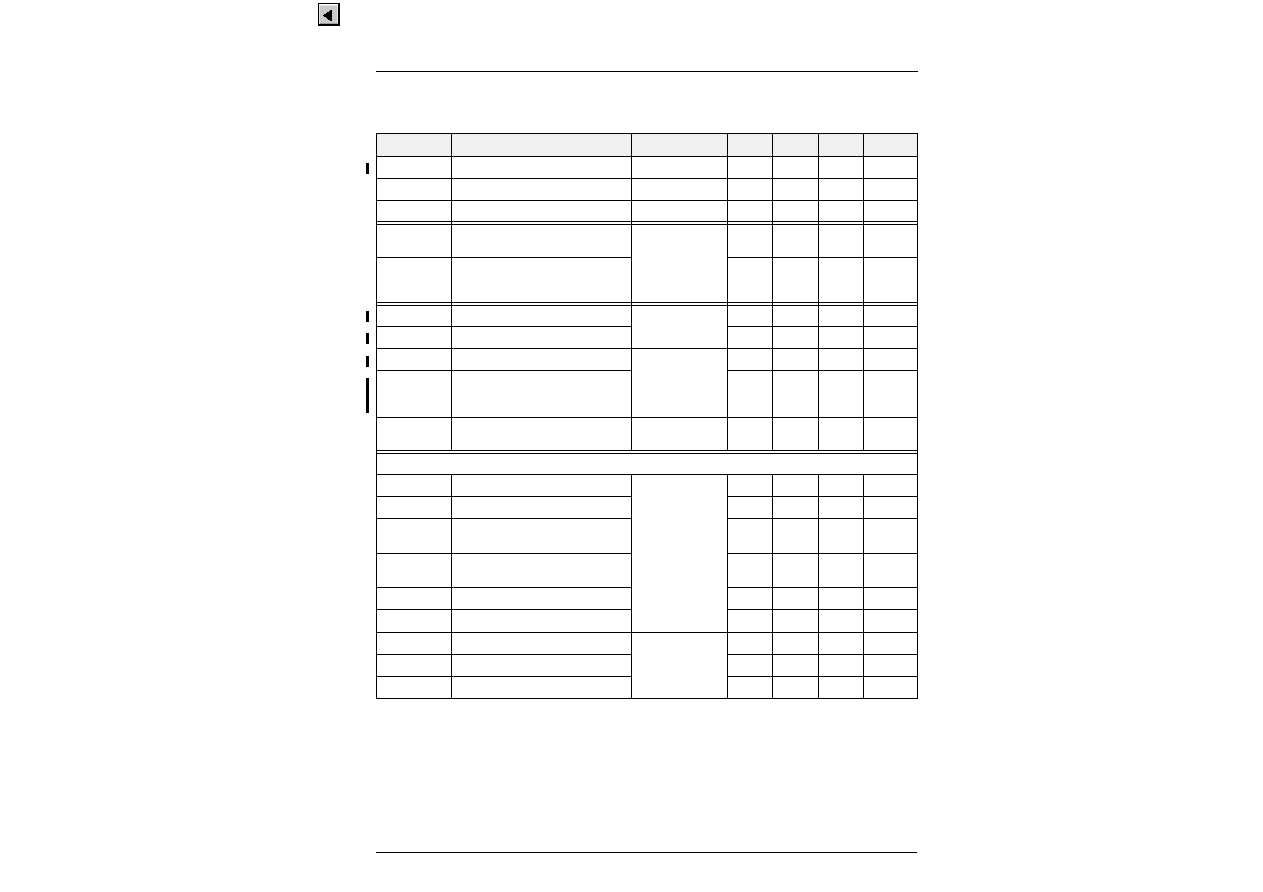
PRELIMINARY DATA SHEET
MSP 34x0D
Micronas
67
9.5.2. Recommended Operating Conditions
(at T
A
= 0 to 70
∞
C)
Symbol
Parameter
Pin Name
Min.
Typ.
Max.
Unit
V
SUP1
First Supply Voltage
AHVSUP
7.6
8.0
8.7
V
V
SUP2
Second Supply Voltage
DVSUP
4.75
5.0
5.25
V
V
SUP3
Third Supply Voltage
AVSUP
4.75
5.0
5.25
V
V
RLH
RESET Input Low-to-High
Transition Voltage
RESETQ
0.7
0.8
DVSUP
V
RHL
RESET Input High-to-Low
Transition Voltage
(see also Fig. 5≠3 on page 20)
0.45
0.55
DVSUP
V
DIGIL
Digital Input Low Voltage
ADR_SEL
0.2
V
SUP2
V
DIGIH
Digital Input High Voltage
0.8
V
SUP2
V
DIGIL
Digital Input Low Voltage
STANDBYQ
0.2
V
SUP2
V
DIGIH
Digital Input High Voltage
MSP 34x0D version A1 to B4
MSP 34x0D version C5 and later
0.8
0.5
V
SUP2
V
SUP2
t
STBYQ1
STANDBYQ Setup Time before
Turn-off of Second Supply Voltage
STANDBYQ,
DVSUP
1
µ
s
I
2
C-Bus Recommendations
V
I2CIL
I
2
C-BUS Input Low Voltage
I2C_CL,
I2C_DA
0.3
V
SUP2
V
I2CIH
I
2
C-BUS Input High Voltage
0.6
V
SUP2
t
I2C5
I
2
C-Data Setup Time Before
Rising Edge of Clock
55
ns
t
I2C6
I
2
C-Data Hold Time after Falling
Edge of Clock
55
ns
t
I2C1
I
2
C START Condition Setup Time
120
ns
t
I2C2
I
2
C STOP Condition Setup Time
120
ns
t
I2C3
I
2
C-Clock Low Pulse Time
I2C_CL
500
ns
t
I2C4
I
2
C-Clock High Pulse Time
500
ns
f
I2C
I
2
C-BUS Frequency
1.0
MHz
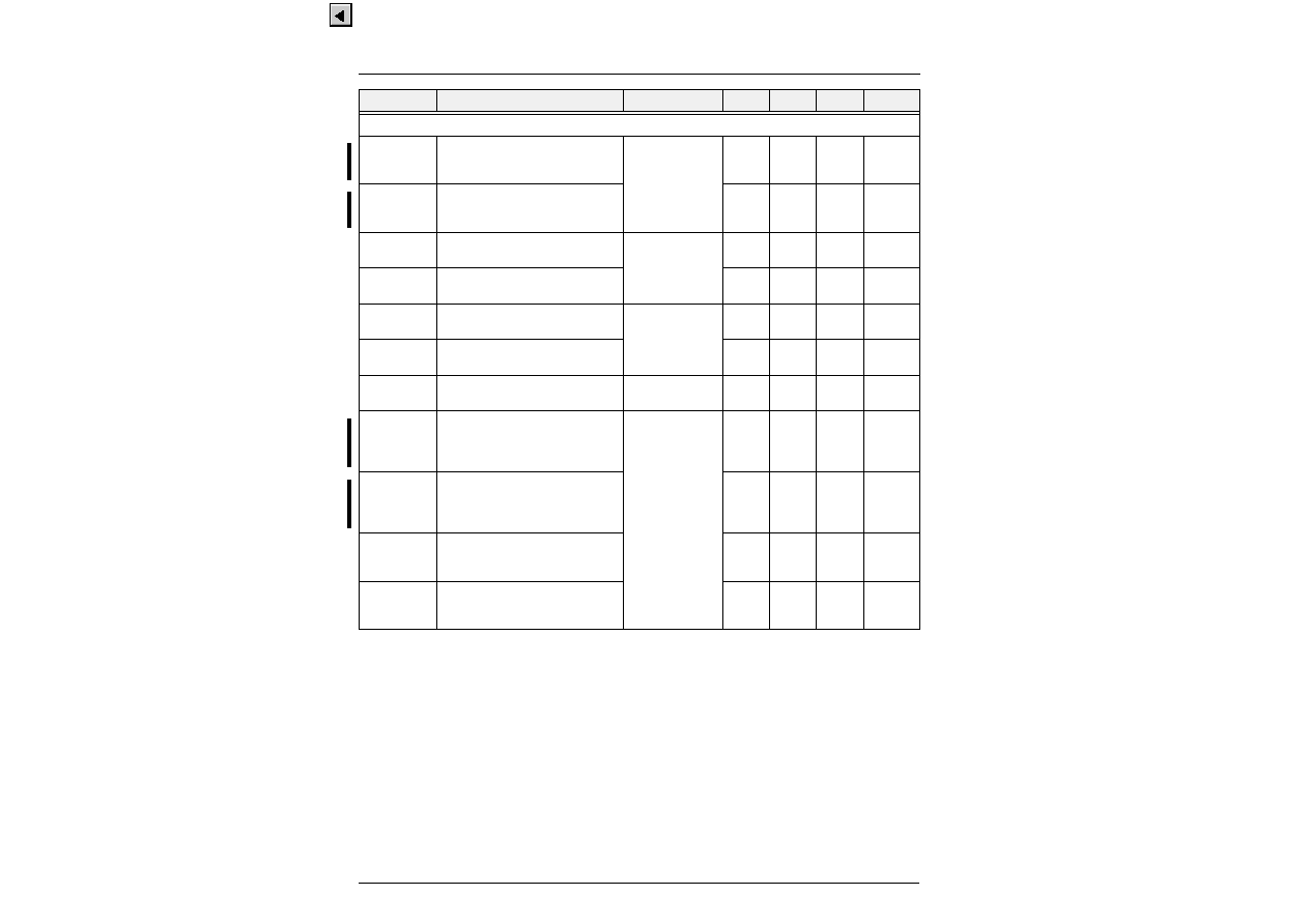
MSP 34x0D
PRELIMINARY DATA SHEET
68
Micronas
I
2
S-Bus Recommendations
V
I2SIH
I
2
S-Data Input High Voltage
MSP 34x0D version A1 to B4
MSP 34x0D version C5 and later
I2S_DA_IN1/2
0.25
0.2
V
SUP2
V
SUP2
V
I2SIL
I
2
S-Data Input Low Voltage
MSP 34x0D version A1 to B4
MSP 34x0D version C5 and later
0.75
0.5
V
SUP2
V
SUP2
t
I2S1
I
2
S-Data Input Setup Time
before Rising Edge of Clock
I2S_DA_IN1/2,
I2S_CL
20
ns
t
I2S2
I
2
S-Data Input Hold Time
after Falling Edge of Clock
0
ns
f
I2SCL
I
2
S-Clock Input Frequency when
MSP in I
2
S-Slave-Mode
I2S_CL
1.024
MHz
R
I2SCL
I
2
S-Clock Input Ratio when
MSP in I
2
S-Slave-Mode
0.9
1.1
f
I2SWS
I
2
S-Word Strobe Input Frequency
when MSP in I
2
S-Slave-Mode
I2S_WS
32.0
kHz
V
I2SIDL
I
2
S-Input Low Voltage when
MSP in I
2
S-Slave Mode
MSP 34x0D version A1 to B4
MSP 34x0D version C5 and later
I2S_CL,
I2S_WS
0.25
0.2
V
SUP2
V
SUP2
V
I2SIDH
I
2
S-Input High Voltage when
MSP in I
2
S-Slave Mode
MSP 34x0D version A1 to B4
MSP 34x0D version C5 and later
0.75
0.5
V
SUP2
V
SUP2
t
I2SWS1
I
2
S-Word Strobe Input Setup Time
before Rising Edge of Clock when
MSP in I
2
S-Slave-Mode
60
ns
t
I2SWS2
I
2
S-Word Strobe Input Hold Time
after Falling Edge of Clock when
MSP in I
2
S-Slave-Mode
0
ns
Symbol
Parameter
Pin Name
Min.
Typ.
Max.
Unit

PRELIMINARY DATA SHEET
MSP 34x0D
Micronas
69
General Crystal Recommendations
f
P
Crystal Parallel Resonance Fre-
quency at 12 pF Load Capacitance
18.432
MHz
R
R
Crystal Series Resistance
8
25
C
0
Crystal Shunt (Parallel) Capacitance
6.2
7.0
pF
C
L
External Load Capacitance
1)
XTAL_IN,
XTAL_OUT
PSDIP
1.5
PLCC
3.3
P(L)QFP
3.3
pF
pF
pF
Crystal Recommendations for Master-Slave Applications
f
TOL
Accuracy of Adjustment
-
20
+20
ppm
D
TEM
Frequency Variation
versus Temperature
-
20
+20
ppm
C
1
Motional (Dynamic) Capacitance
19
24
fF
f
CL
Required Open Loop Clock
Frequency (T
amb
= 25
∞
C)
AUD_CL_OUT
18.431
18.433
MHz
Crystal Recommendations for FM / NICAM Applications (No Master-Slave Mode possible)
f
TOL
Accuracy of Adjustment
-
30
+30
ppm
D
TEM
Frequency Variation vs. Temp.
-
30
+30
ppm
C
1
Motional (Dynamic) Capacitance
15
fF
f
CL
Required Open Loop Clock
Frequency (T
amb
= 25
∞
C)
AUD_CL_OUT
18.4305
18.4335
MHz
Crystal Recommendations for FM Applications (No Master-Slave Mode possible)
f
TOL
Accuracy of Adjustment
-
100
+100
ppm
D
TEM
Frequency Variation
versus Temperature
-
50
+50
ppm
Amplitude Recommendation for Operation with External Clock Input (C
load
after reset = 22 pF)
V
XCA
External Clock Amplitude
XTAL_IN
0.7
V
pp
1)
External capacitors at each crystal pin to ground are required. They are necessary to tune the open-loop fre-
quency of the internal PLL and to stabilize the frequency in closed-loop operation.
Due to different layouts, the accurate capacitor size should be determined with the customer PCB. The sug-
gested values (1.5...3.3 pF) are figures based on experience and should serve as "start value".
To define the capacitor size, reset the MSP without transmitting any further I
2
C telegrams. Measure the fre-
quency at AUD_CL_OUT-pin. Change the capacitor size until the free running frequency matches 18.432 MHz
as closely as possible.The higher the capacity, the lower the resulting clock frequency.
Symbol
Parameter
Pin Name
Min.
Typ.
Max.
Unit
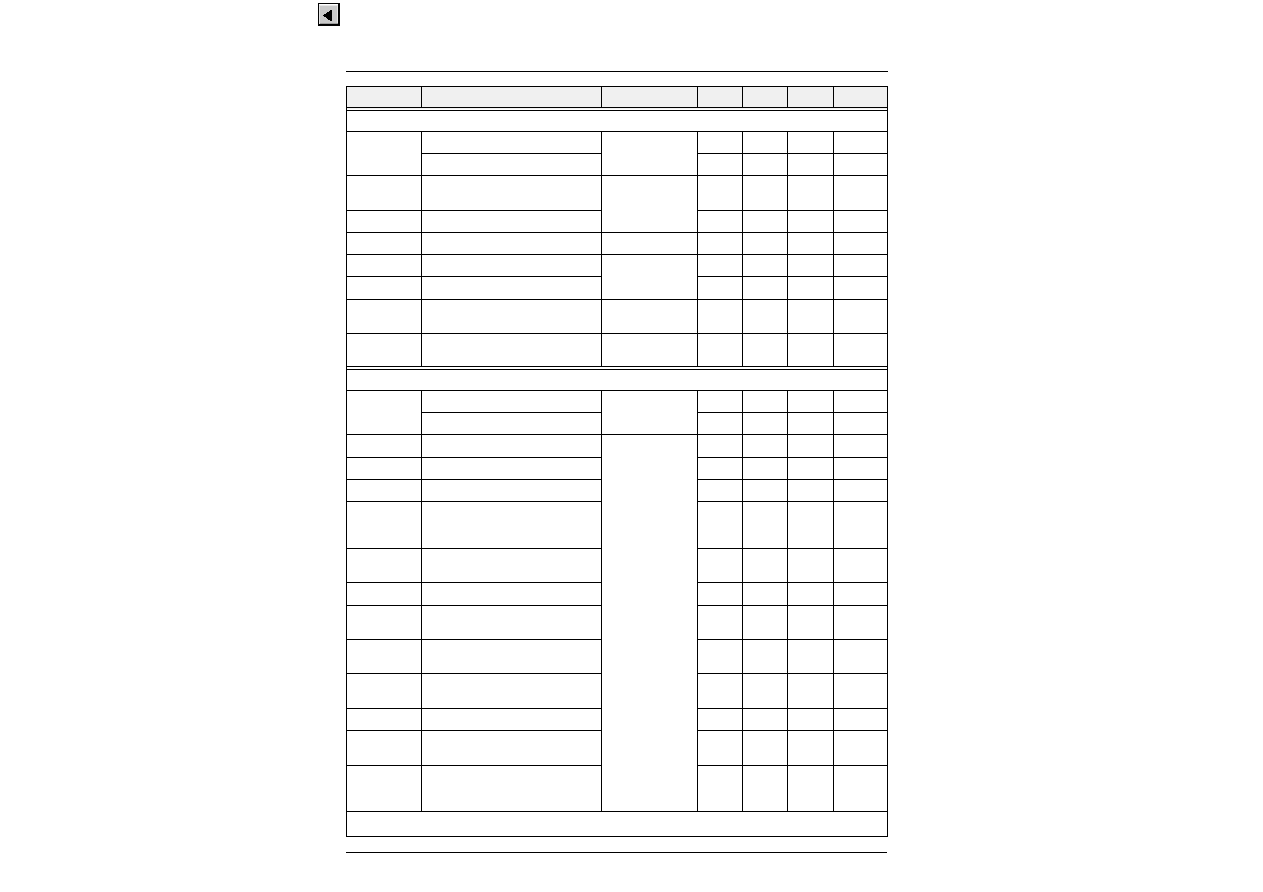
MSP 34x0D
PRELIMINARY DATA SHEET
70
Micronas
Analog Input and Output Recommendations
C
AGNDC
AGNDC Filter Capacitor
AGNDC
-
20%
3.3
µ
F
Ceramic Capacitor in Parallel
-
20%
100
nF
C
inSC
DC-Decoupling Capacitor
in front of SCART Inputs
SCn_IN_s
1)
-
20%
330
+20%
nF
V
inSC
SCART Input Level
2.0
V
RMS
V
inMONO
Input Level, Mono Input
MONO_IN
2.0
V
RMS
R
LSC
SCART Load Resistance
SCn_OUT_s
1)
10
k
C
LSC
SCART Load Capacitance
6.0
nF
C
VMA
Main/AUX Volume Capacitor
CAPL_M,
CAPL_A
10
µ
F
C
FMA
Main/AUX Filter Capacitor
DACM_s,
DACA_s
1)
-
10%
1
+10%
nF
Recommendations for Analog Sound IF Input Signal
C
VREFTOP
VREFTOP Filter Capacitor
VREFTOP
-
20%
10
µ
F
Ceramic Capacitor in Parallel
-
20%
100
nF
F
IF_FM
Analog Input Frequency Range
ANA_IN1+,
ANA_IN2+,
ANA_IN-
0
9
MHz
V
IF_FM
Analog Input Range FM/NICAM
0.1
0.8
3
V
pp
V
IF_AM
Analog Input Range AM/NICAM
0.1
0.45
0.8
V
pp
R
FMNI
Ratio: NICAM Carrier/FM Carrier
(unmodulated carriers)
BG:
I:
-
20
-
23
-
7
-
10
0
0
dB
dB
R
AMNI
Ratio: NICAM Carrier/AM Carrier
(unmodulated carriers)
-
25
-
11
0
dB
R
FM
Ratio: FM-Main/FM-Sub Satellite
7
dB
R
FM1/FM2
Ratio: FM1/FM2
German FM System
7
dB
R
FC
Ratio: Main FM Carrier/
Color Carrier
15
-
-
dB
R
FV
Ratio: Main FM Carrier/
Luma Components
15
-
-
dB
PR
IF
Pass-band Ripple
-
-
±
2
dB
SUP
HF
Suppression of Spectrum
Above 9.0 MHz
15
-
dB
FM
MAX
Maximum FM Deviation (approx.)
normal mode
high deviation mode
±
192
±
360
kHz
1)
"n" means "1", "2" or "3", "s" means "L" or "R"
Symbol
Parameter
Pin Name
Min.
Typ.
Max.
Unit

PRELIMINARY DATA SHEET
MSP 34x0D
Micronas
71
9.5.3. Characteristics
at T
A
= 0 to 70
∞
C, f
CLOCK
= 18.432 MHz, V
SUP1
= 7.6 to 8.7 V, V
SUP2
= 4.75 to 5.25 V for min./max. values
at T
A
= 60
∞
C, f
CLOCK
= 18.432 MHz, V
SUP1
= 8 V, V
SUP2
= 5 V for typical values, T
J
= Junction Temperature
MAIN (M) = Loudspeaker Channel, AUX (A) = Headphone Channel
Symbol
Parameter
Pin Name
Min.
Typ.
Max.
Unit
Test Conditions
f
CLOCK
Clock Input Frequency
XTAL_IN
18.432
MHz
D
CLOCK
Clock High to Low Ratio
45
55
%
t
JITTER
Clock Jitter
(verification not
provided in production test)
50
ps
V
xtalDC
DC-Voltage Oscillator
2.5
V
t
Startup
Oscillator
Start-up Time
at
V
DD
Slew-rate of 1 V/1
µ
s
XTAL_IN,
XTAL_OUT
0.4
2
ms
I
SUP1A
First Supply Current (active)
Analog Volume for Main and Aux at 0 dB
Analog Volume for Main and Aux at
-
30 dB
AHVSUP
9.6
6.3
17.1
11.2
24.6
16.1
mA
mA
I
SUP1S
First Supply Current
(standby mode) at T
j
= 27
∞
C
3.5
5.6
7.7
mA
STANDBYQ = low
I
SUP2A
Second Supply Current (active)
MSP 34x0D version A1 to B4
MSP 34x0D version C5 and later
DVSUP
86
50
95
70
110
85
mA
mA
I
SUP3A
Third Supply Current (active)
MSP 34x0D version A1 to B4
MSP 34x0D version C5 and later
AVSUP
15
20
25
35
35
45
mA
mA
V
ACLKAC
Audio Clock Output AC Voltage
AUD_CL_OUT
1.2
1.8
V
pp
load = 40 pF
V
ACLKDC
Audio Clock Output DC Voltage
0.4
0.6
V
SUP3
I
max
= 0.2 mA
r
outHF_ACL
HF Output Resistance
140
a
ACL
Open Circuit Gain
AUD_CL_OUT,
XTAL_OUT
0.5
Digital Control Outputs
V
DCTROL
Digital Output Low Voltage
D_CTR_OUT0,
D_CTR_OUT1
0.4
V
I
DCTR
= 1 mA
V
DCTROH
Digital Output High Voltage
4.0
V
I
DCTR
=
-
1 mA
I
2
C-Bus
V
I2COL
I
2
C-Data Output Low Voltage
I2C_DA
0.4
V
I
I2COL
= 3 mA
I
I2COH
I
2
C-Data Output High Current
1.0
µ
A
V
I2COH
= 5 V
t
I2COL1
I
2
C-Data Output Hold Time
after Falling Edge of Clock
I2C_DA,
I2C_CL
15
ns
t
I2COL2
I
2
C-Data Output Setup Time
before Rising Edge of Clock
100
ns
f
I2C
= 1 MHz
I
2
S-Bus
V
I2SOL
I
2
S-Output Low Voltage
I2S_WS,
I2S_CL,
I2S_DA_OUT
0.4
V
I
I2SOL
= 1 mA
V
I2SOH
I
2
S-Output High Voltage
4.0
V
I
I2SOH
=
-
1 mA
f
I2SCL
I
2
S-Clock Output Frequency
I2S_CL
1024
kHz
NICAM-PLL closed
f
I2SWS
I
2
S-Word Strobe Output Frequency
I2S_WS
32.0
kHz
NICAM-PLL closed
t
I2S1/I2S2
I
2
S-Clock High/Low-Ratio
I2S_CL
0.9
1.0
1.1
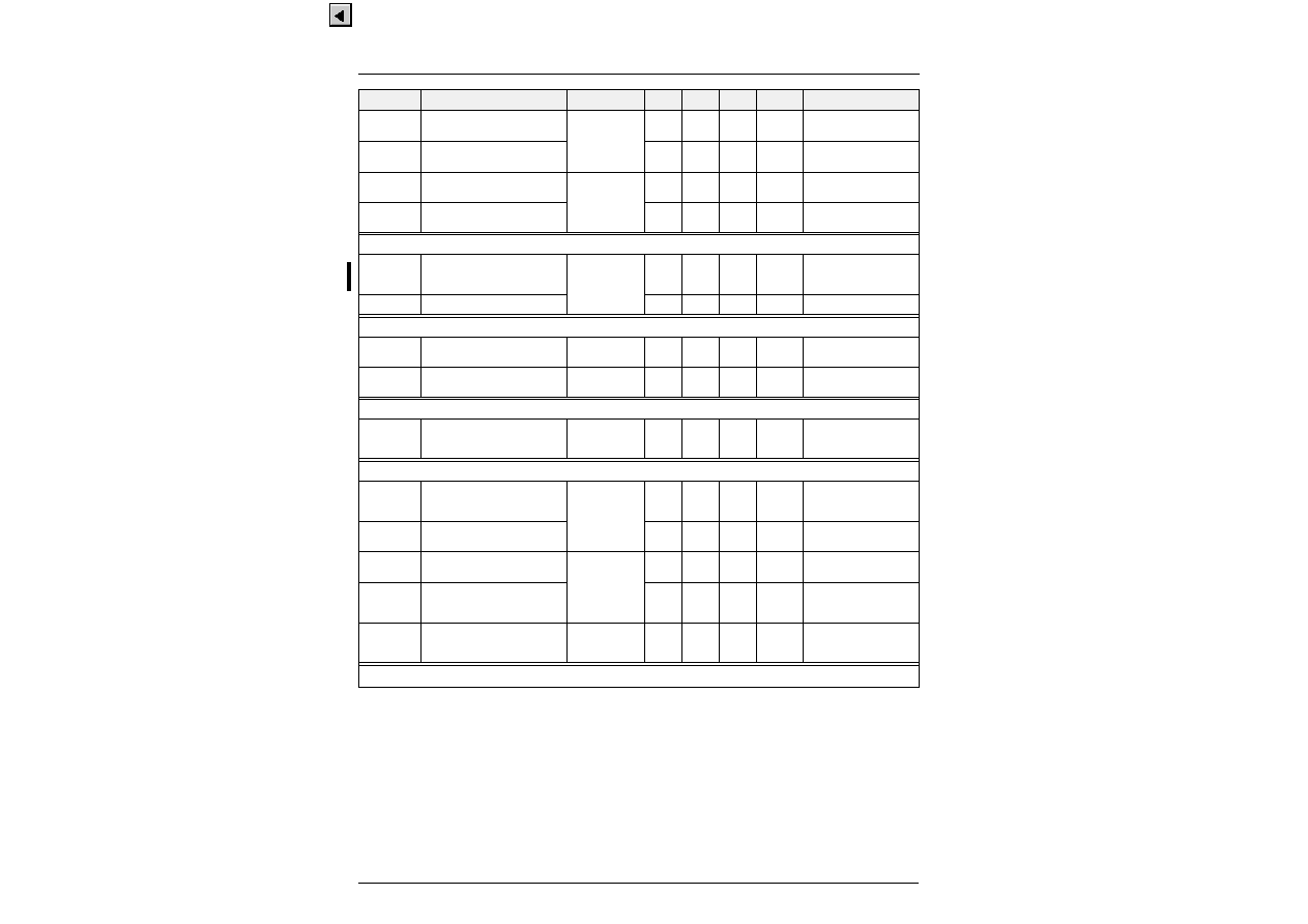
MSP 34x0D
PRELIMINARY DATA SHEET
72
Micronas
t
I2S3
I
2
S-Data Setup Time
before Rising Edge of Clock
I2S_CL,
I2S_DA_OUT
200
ns
C
L
= 30 pF
t
I2S4
I
2
S-Data Hold Time
after Falling Edge of Clock
180
ns
C
L
= 30 pF
t
I2S5
I
2
S-Word Strobe Setup Time
before Rising Edge of Clock
I2S_CL,
I2S_WS
200
ns
C
L
= 30 pF
t
I2S6
I
2
S-Word Strobe Hold Time
after Falling Edge of Clock
180
ns
C
L
= 30 pF
Analog Ground
V
AGNDC0
AGNDC Open Circuit Voltage
MSP 34x0D version A1 to B4
MSP 34x0D version C5 and later
AGNDC
3.63
3.67
3.73
3.77
3.83
3.87
V
V
R
load
10 M
R
outAGN
AGNDC Output Resistance
70
125
180
k
3 V
V
AGNDC
4 V
Analog Input Resistance
R
inSC
SCART Input Resistance
from T
A
= 0 to 70
∞
C
SCn_IN_s
1)
25
40
58
k
f
signal
= 1 kHz, I = 0.05 mA
R
inMONO
MONO Input Resistance
from T
A
= 0 to 70
∞
C
MONO_IN
15
24
35
k
f
signal
= 1 kHz, I = 0.1 mA
Audio Analog-to-Digital-Converter
V
AICL
Effective Analog Input Clipping
Level for Analog-to-Digital-
Conversion
SCn_IN_s,
1)
MONO_IN
2.00
2.25
V
RMS
f
signal
= 1 kHz
SCART Outputs
R
outSC
SCART Output Resistance
at T
j
= 27
∞
C
from T
A
= 0 to 70
∞
C
SCn_OUT_s
1)
200
200
330
460
500
f
signal
= 1 kHz, I = 0.1 mA
dV
OUTSC
Deviation of DC-Level at SCART
Output from AGNDC Voltage
-
70
+70
mV
A
SCtoSC
Gain from Analog Input
to SCART Output
SCn_IN_s
1)
MONO_IN
SCn_OUT_s
1)
-
1.0
+0.5
dB
f
signal
= 1 kHz
f
rSCtoSC
Frequency Response from Analog
Input to SCART Output
bandwidth: 0 to 20000 Hz
-
0.5
+0.5
dB
with respect to 1 kHz
V
outSC
Effective Signal Level at
SCART-Output during full-scale
digital input signal from DSP
SCn_OUT_s
1)
1.8
1.9
2.0
V
RMS
f
signal
= 1 kHz
1)
"n" means "1", "2", "3", or "4"; "s" means "L" or "R"
Symbol
Parameter
Pin Name
Min.
Typ.
Max.
Unit
Test Conditions

PRELIMINARY DATA SHEET
MSP 34x0D
Micronas
73
Main and AUX Outputs
R
outMA
Main/AUX Output Resistance
at T
j
= 27
∞
C
from T
A
= 0 to 70
∞
C
DACp_s
1
)
2.1
2.1
3.3
4.6
5.0
k
k
f
signal
= 1 kHz, I = 0.1 mA
V
outDCMA
DC-Level at Main/AUX-Output
for Analog Volume at 0 dB
for Analog Volume at
-
30 dB
1.80
2.04
61
2.28
V
mV
V
outMA
Effective Signal Level at Main/
AUX-Output during full-scale digital
input signal from DSP for Analog
Volume at 0 dB
1.23
1.37
1.51
V
RMS
f
signal
= 1 kHz
Analog Performance
SNR
Signal-to-Noise Ratio
from Analog Input to DSP
MONO_IN,
SCn_IN_s
1)
85
88
dB
Input Level =
-
20 dB with
resp. to V
AICL
, f
sig
= 1 kHz,
equally weighted
20 Hz...16 kHz
2)
from Analog Input to
SCART Output
MONO_IN,
SCn_IN_s
1)
SCn_OUT_s
1)
93
96
dB
Input Level =
-
20 dB,
f
sig
= 1 kHz,
equally weighted
20 Hz...20 kHz
from DSP to SCART Output
SCn_OUT_s
1)
85
88
dB
Input Level =
-
20 dB,
f
sig
= 1 kHz,
equally weighted
20 Hz...15 kHz
3)
from DSP to Main/AUX-Output
for Analog Volume at 0 dB
for Analog Volume at
-
30 dB
DACp_s
1)
85
78
88
83
dB
dB
Input Level =
-
20 dB,
f
sig
= 1 kHz,
equally weighted
20 Hz...15 kHz
3)
THD
Total Harmonic Distortion
from Analog Input to DSP
MONO_IN,
SCn_IN_s
1)
0.01
0.03
%
Input Level =
-
3 dBr with
resp. to V
AICL
, f
sig
= 1 kHz,
equally weighted
20 Hz...16 kHz
2)
from Analog Input to
SCART Output
MONO_IN,
SCn_IN_s
SCn_OUT_s
1)
0.01
0.03
%
Input Level =
-
3 dBr,
f
sig
= 1 kHz,
equally weighted
20 Hz...20 kHz
from DSP to SCART Output
SCn_OUT_s
1)
0.01
0.03
%
Input Level =
-
3 dBr,
f
sig
= 1 kHz,
equally weighted
20 Hz...16 kHz
3)
from DSP to Main or AUX Output
DACA_s,
DACM_s
1)
0.01
0.03
%
Input Level =
-
3 dBr,
f
sig
= 1 kHz,
equally weighted
20 Hz...16 kHz
3)
1)
"n" means "1", "2", "3", or "4"; "s" means "L" or "R"; "p" means "M" or "A"
2)
DSP measured at I
2
S-Output
3)
DSP Input at I
2
S-Input
Symbol
Parameter
Pin Name
Min.
Typ.
Max.
Unit
Test Conditions

MSP 34x0D
PRELIMINARY DATA SHEET
74
Micronas
XTALK
Crosstalk attenuation
-
PLCC68
-
PSDIP64
Input Level =
-
3 dB,
f
sig
= 1 kHz, unused ana-
log inputs connected to
ground by Z < 1 k
between left and right channel within
SCART Input/Output pair (L
R, R
L)
SCn_IN
SCn_OUT
1)
PLCC68
PSDIP64
SC1_IN or SC2_IN
DSP
PLCC68
PSDIP64
SC3_IN
DSP
PLCC68
PSDIP64
DSP
SCn_OUT
1)
PLCC68
PSDIP64
80
80
80
80
80
80
80
80
dB
dB
dB
dB
dB
dB
dB
dB
equally weighted
20 Hz...20 kHz
2)
3)
between left and right channel within
Main or AUX Output pair
DSP
DACp
1)
PLCC68
PSDIP64
80
75
dB
dB
equally weighted
20 Hz...16 kHz
3)
between SCART Input/Output pairs
1)
D = disturbing program
O = observed program
D: MONO/SCn_IN
SCn_OUT
PLCC68
O: MONO/SCn_IN
SCn_OUT
1)
PSDIP64
D: MONO/SCn_IN
SCn_OUT or unsel.
PLCC68
O: MONO/SCn_IN
DSP
1)
PSDIP64
D: MONO/SCn_IN
SCn_OUT
PLCC68
O: DSP
SCn_OUT
1)
PSDIP64
D: MONO/SCn_IN
unselected
PLCC68
O: DSP
SC1_OUT
PSDIP64
100
100
100
95
100
100
100
100
dB
dB
dB
dB
dB
dB
dB
dB
(equally weighted
20 Hz...20 kHz
same signal source on left
and right disturbing chan-
nel, effect on each
observed output channel
2)
3)
3)
Crosstalk between Main and AUX Output pairs
DSP
DACp
1)
PLCC68
PSDIP64
95
90
dB
dB
(equally weighted
20 Hz...16 kHz)
3)
same signal source on left
and right disturbing chan-
nel, effect on each
observed output channel
XTALK
Crosstalk from Main or AUX Output to SCART Output
and vice-versa
D = disturbing program
O = observed program
D: MONO/SCn_IN/DSP
SCn_OUT
PLCC68
O: DSP
DACp
1)
PSDIP64
D: MONO/SCn_IN/DSP
SCn_OUT
PLCC68
O: DSP
DACp
1)
PSDIP64
D: DSP
DACp
PLCC68
O: MONO/SCn_IN
SCn_OUT
1)
PSDIP64
D: DSP
DACM
PLCC68
O: DSP
SCn_OUT
1)
PSDIP64
85
80
90
85
100
95
100
95
dB
dB
dB
dB
dB
dB
dB
dB
(equally weighted
20 Hz...20 kHz)
same signal source on left
and right disturbing chan-
nel, effect on each
observed output channel
SCART output load resis-
tance 10 k
SCART output load resis-
tance 30 k
3)
1)
"n" means "1", "2", "3", or "4"; "p" means "M" or "A"
2)
DSP measured at I
2
S-Output
3)
DSP Input at I
2
S-Input
Symbol
Parameter
Pin Name
Min.
Typ.
Max.
Unit
Test Conditions

PRELIMINARY DATA SHEET
MSP 34x0D
Micronas
75
PSRR: rejection of noise on AHVSUP at 1 kHz
AGNDC
AGNDC
80
dB
From Analog Input to DSP
MONO_IN,
SCn_IN_s
1)
70
dB
From Analog Input to
SCART Output
MONO_IN,
SCn_IN_s
1)
,
SCn_OUT_s
1)
70
dB
From DSP to SCART Output
SCn_OUT_s
1)
60
dB
From DSP to MAIN/AUX Output
DACp_s
1)
80
dB
S/N
FM
FM Input to Main/AUX/SCART
Output
DACp_s
1)
,
SCn_OUT_s
1)
73
dB
1 FM-carrier 5.5 MHz,
50
µ
s, 1 kHz, 40 kHz devi-
ation; RMS, unweighted 0
to 15 kHz (for S/N);
full input range,
FM-Prescale = 46
h
,
Vol = 0 dB
Output Level 1 V
RMS
at
DACp_s
1)
; SPM = 3
THD
FM
Total Harmonic Distortion + Noise
of FM demodulated signal on Main/
AUX/SCART output
DACp_s
1)
,
SCn_OUT_s
1)
0.1
%
S/N
NICAM
Signal to Noise ratio of NICAM
baseband signal on Main/AUX/
SCART outputs
DACp_s
1)
,
SCn_OUT_s
1)
72
dB
NICAM:
-
6 dB, 1 kHz,
RMS unweighted
0 to 15 kHz, Vol = 9 dB
NIC_Presc = 7F
h
Output level 1 V
RMS
at
DACp_s
1)
;
SPM = 8
THD
NICAM
Total Harmonic Distortion + Noise
of NICAM baseband signal on
Main/AUX/SCART output
DACp_s
1)
,
SCn_OUT_s
1)
0.1
%
2.12 kHz, Modulator input
level = 0 dBref
SPM = 8
BER
NI
NICAM: Bit Error Rate
-
1
10
-
7
FM+NICAM,
norm conditions
S/N
AM
Signal to Noise ratio of AM base-
band signal on Main/AUX/SCART
outputs
DACp_s
1)
,
SCn_OUT_s
1)
48
dB
SIF input range:
0.1
-
0.8 V
pp
; AM = 70 %,
1 kHz, RMS unweighted
(S/N); 0 to 15 kHz,
FM/AM-Prescale = 3C
hex
,
Vol = 0 dB
Output level:
0.5 V
RMS
at DACp_s
1)
FM+NICAM, norm condi-
tions; SPM = 9
THD
AM
Total Harmonic Distortion + Noise
of AM demodulated signal on Main/
AUX/SCART output
DACp_s
1)
,
SCn_OUT_s
1)
0.3
%
1)
"n" means "1", "2", "3", or "4"; "s" means "L" or "R"; "p" means "Loudspeaker (Main)'' or ``Headphone (AUX)''
SPM: Short Programming Mode
Symbol
Parameter
Pin Name
Min.
Typ.
Max.
Unit
Test Conditions
MSP 34x0D
PRELIMINARY DATA SHEET
76
Micronas
R
IFIN
Input Impedance
ANA_IN1+,
ANA_IN2+,
ANA_IN
-
1.5
6.8
2
9.1
2.5
11.4
k
k
Gain AGC = 20 dB
Gain AGC = 3 dB
DC
VREFTOP
DC voltage at VREFTOP
MSP 34x0D version A1 to B4
MSP 34x0D version C5 and later
VREFTOP
2.4
2.56
2.6
2.66
2.7
2.76
V
V
DC
ANA_IN
DC voltage on IF inputs
ANA_IN1+,
ANA_IN2+,
ANA_IN
-
1.3
1.5
1.7
V
XTALK
IF
Crosstalk attenuation
ANA_IN1+,
ANA_IN2+,
ANA_IN
-
40
dB
f
signal
= 1 MHz
Input Level =
-
2 dBr
BW
IF
3 dB Bandwidth
10
MHz
AGC
AGC Step Width
0.85
dB
dV
FMOUT
Tolerance of output voltage
of FM demodulated signal
DACp_s
1)
,
SCn_OUT_s
1)
-
1.5
+1.5
dB
1 FM-carrier, 50
µ
s, 1 kHz,
40 kHz deviation; RMS
dV
NICAMOUT
Tolerance of output voltage
of NICAM baseband signal
DACp_s
1)
,
SCn_OUT_s
1)
-
1.5
+1.5
dB
2.12 kHz, Modulator input
level = 0 dBref
fR
FM
FM Frequency Response on Main/
AUX/SCART Outputs,
Bandwidth 20 to 15000 Hz
DACp_s
1)
,
SCn_OUT_s
1)
-
1.0
+1.0
dB
1 FM-carrier 5.5 MHz,
50
µ
s, Modulator input
level =
-
14.6 dBref; RMS
fR
NICAM
NICAM Frequency Response on
Main/AUX/SCART Outputs,
Bandwidth 20 to 15000 Hz
DACp_s
1)
,
SCn_OUT_s
1)
-
1.0
+1.0
dB
Modulator input
level =
-
12 dB dBref; RMS
SEP
FM
FM Channel Separation (Stereo)
DACp_s
1)
,
SCn_OUT_s
1)
50
dB
2 FM-carriers
5.5/5.74 MHz, 50
µ
s,
1 kHz, 40 kHz deviation;
RMS
SEP
NICAM
NICAM Channel Separation
(Stereo)
DACp_s
1)
,
SCn_OUT_s
1)
80
dB
XTALK
FM
FM Crosstalk Attenuation (Dual)
DACp_s
1)
,
SCn_OUT_s
1)
80
dB
2 FM-carriers
5.5/5.74 MHz, 50
µ
s,
1 kHz, 40 kHz deviation;
RMS
XTALK
NICAM
NICAM Crosstalk Attenuation
(Dual)
DACp_s
1)
,
SCn_OUT_s
1)
80
dB
1)
"n" means "1", "2", "3", or "4"; "s" means "L" or "R"; "p" means "M" or "A"
Symbol
Parameter
Pin Name
Min.
Typ.
Max.
Unit
Test Conditions

PRELIMINARY DATA SHEET
MSP 34x0D
Micronas
77
10. Application Circuit
SC1_OUT_L (37) 47
SC1_OUT_R (36) 48
SC2_OUT_L (34) 50
SC2_OUT_R (33) 51
45
(39
)
A
H
V
S
U
P
43
(41
)
A
H
V
S
S
2
6
(
5
7
)
AV
SUP
67
(18
)
D
V
S
U
P
66
(19
)
D
V
S
S
61
(24
)
R
E
S
E
TQ
2
7
(
5
6
)
AV
SS
49
(35
)
V
R
E
F
1
58
(27
)
V
R
E
F
2
5 V
5 V
8.0 V
A
VSS
5 V
5 V
C
A
P
L_M (
40)
44
C
A
P
L
_
A
(
38)
46
V
R
E
F
T
O
P
(
54)
29
A
G
N
D
C
(
42)
42
A
N
A
_
IN
1
+
(
58)
25
A
N
A
_
IN
2
+
(
60)
23
ANA_
I
N
-
(
59)
24
X
T
A
L_IN
(
62)
21
X
T
A
L
_OU
T
(
63)
20
ResetQ
(from CCU,
see section.
5.3. )
MSP 34x0D
D_CTR_OUT0 (5) 13
D_CTR_OUT1 (4) 14
AUD_CL_OUT (1) 18
TESTEN (61) 22
+
100
100
100
100
22
µ
F
22
µ
F
22
µ
F
22
µ
F
+
+
+
DACA_R (25) 60
1 nF
1 nF
1 nF
1 nF
1 nF
DACA_L (26) 59
DACM_SUB (31) 54
DACM_R (28) 57
DACM_L (29) 56
1
µ
F
1
µ
F
1
µ
F
1
µ
F
1
µ
F
Headphones
Loudspeaker
Tuner 1
Tuner 2
IF2 IN
Signal GND
IF1 IN
56 pF
56 pF
56 pF
+
3.3
µ
F
100
nF
100
nF
10
µ
F
+
-
if ANA_IN2+ not used
+8.0 V
18
.432
MH
z
+
+
10
µ
F 10
µ
F
28 (55) MONO_IN
31 (52) SC1_IN_L
30 (53) SC1_IN_R
32 (51) ASG1
34 (49) SC2_IN_L
33 (50) SC2_IN_R
35 (48) ASG2
37 (46) SC3_IN_L
36 (47) SC3_IN_R
38 (45) ASG4
40 (43) SC4_IN_L
39 (44) SC4_IN_R
11 (7) STANDBYQ
12 (6) ADR_SEL
8 (10) I2C_DA
9 (9) I2C_CL
1 (16) ADR_WS
68 (17) ADR_CL
3 (15) ADR_DA
6 (12) I2S_WS
7 (11) I2S_CL
4 (14) I2S_DA_IN1
65 (20) I2S_DA_IN2
5 (13) I2S_DA_OUT
100
nF
100
nF
100
nF
Alternative circuit for
ANA_IN1/2+ for more
attenuation of video
100 p
56 p
1 k
ANA_IN1/2+
AHVSS
AHVSS
AHVSS
330 nF
330 nF
330 nF
330 nF
330 nF
330 nF
330 nF
330 nF
330 nF
DVSS
DVSS
AVSS
components:
C see section 9.5.2.
*
DVSS
A
H
VSS

MSP 34x0D
PRELIMINARY DATA SHEET
78
Micronas
Note: Pin numbers refer to the PLCC68 package; numbers in brackets refer to the PSDIP64 package.
*Application Note:
All ground pins should be connected to one low-resis-
tive ground plane.
All supply pins should be connected separately with
short and low-resistive lines to the power supply.
Decoupling capacitors from DVSUP to DVSS, AVSUP
to AVSS, and AHVSUP to AHVSS are recommended
as closely as possible to these pins. Decoupling of
DVSUP and DVSS is most important. We recommend
using more than one capacitor. By choosing different
values, the frequency range of active decoupling can
be extended. In our application boards we use: 220 pF,
470 pF, 1.5 nF, and 10
µ
F. The capacitor with the low-
est value should be placed nearest to the DVSUP and
DVSS pins.
The ASG pins should be connected as closely as pos-
sible to the MSP to ground. If they are lead with the
SCART input lines as shielding line, they should NOT
be connected to ground at the SCART connector.

PRELIMINARY DATA SHEET
MSP 34x0D
Micronas
79
11. Appendix A: MSP 34x0D Version History
A1
First hardware release, which is completely compatible
to MSP 3410B.
A2
Hardware as A1 with additional features:
≠ Automatic NICAM-FM switching
≠ Demodulator Short Programming
≠ Automatic Standard Detection
B3
Hardware as A2 with additional features:
≠ Automatic Volume Correction (AVC)
≠ Subwoofer Output
≠ improved Automatic Standard Detection
≠ extended Short Programming Mode
≠ automatic reset and selection of identification for
Demodulator Short Programming
B4
Hardware and firmware as B3:
≠ Carrier Mute Function not recommended in High-
Deviation Mode
C5
≠ additional package PLQFP64
≠ digital input specification changed as of version C5
and later (see section 9.5. on page 66)
≠ max. analog high supply voltage AHVSUP 8.7 V
≠ supply currents changed as of version C5 and later
(see section 9.5.3. on page 71)
≠ Pin ASG3 no longer supported

MSP 34x0D
PRELIMINARY DATA SHEET
80
Micronas
All information and data contained in this data sheet are without any
commitment, are not to be considered as an offer for conclusion of a
contract, nor shall they be construed as to create any liability. Any new
issue of this data sheet invalidates previous issues. Product availability
and delivery are exclusively subject to our respective order confirmation
form; the same applies to orders based on development samples deliv-
ered. By this publication, Micronas GmbH does not assume responsibil-
ity for patent infringements or other rights of third parties which may
result from its use.
Further, Micronas GmbH reserves the right to revise this publication and
to make changes to its content, at any time, without obligation to notify
any person or entity of such revisions or changes.
No part of this publication may be reproduced, photocopied, stored on a
retrieval system, or transmitted without the express written consent of
Micronas GmbH.
Micronas GmbH
Hans-Bunte-Strasse 19
D-79108 Freiburg (Germany)
P.O. Box 840
D-79008 Freiburg (Germany)
Tel. +49-761-517-0
Fax +49-761-517-2174
E-mail: docservice@micronas.com
Internet: www.micronas.com
Printed in Germany
Order No. 6251-482-2PD
12. Data Sheet History
1. Preliminary data sheet: "MSP 3400D, MSP 3410D
Multistandard Sound Processors, Nov. 30, 1998,
6251-482-1PD. First release of the preliminary data
sheet.
2. Preliminary data sheet: "MSP 3400D, MSP 3410D
Multistandard Sound Processors, May 14, 1999,
6251-482-2PD. Second release of the preliminary
data sheet. Major changes:
≠ specification for version C5 added
(see Appendix A: Version History)
≠ section 9.: specification for PLQFP64 package
added

Micronas
page 1 of 1
Subject:
Data Sheet Concerned:
Supplement:
Edition:
Preliminary Data Sheet Supplement
MSP 34xxD Family Compatibility Differences:
The MSP-family (MSP 3410D, MSP 3400D, MSP 3415D, MSP 3405D, MSP 3417D, MSP 3407D) is currently avail-
able in different technologies (0.8 µ, 0.5 µ, and 0.45 µ).
The specific differences of the various implementations are listed in the attached table.
Compatibility Differences
All MSP 34xxD Data Sheets:
6251-482-2PD, 6251-475-2PD, 6251-486-2PD
No. 3/ 6251-526-3PDS
Oct. 11, 2000
MSP 34xxD

Micronas
Compatibility Differences between 0.5/0.45µ and 0.8µ MSPD Devices
B4
A2
A1
0.8µ
0.5µ
0.45µ
0.8µ
0.5µ
0.45µ
0.8µ
0.5µ
0.45µ
67, 6B, 6G
8C and 94
G1, G4
H1, H3
6C, 6D
8D
G2, G5
H2, H4
6E, 6F
8F
G3, G6,
H5
Feature
Documented in
Datasheet Reference
General Hardware
Power Consumption
Datasheet
910 mW
640 mW
600 mW
910 mW
640 mW
600 mW
910 mW
640 mW
600 mW
Total Electromagnetic Radiation (EMR)
-
-
-
V
AGNDC0
typical
Datasheet
3.73 V
3.73 V
3.73 V
DC
VREFTOP
typical
Datasheet
2.6 V
2.6 V
2.6 V
Maximum V
sup1
Datasheet
8.4 V
8.4 V
8.4 V
Digital Input Pin characteristics
(I2S_IN1/2, I2S_WS/CL, StANDBYQ)
Datasheet
-
-
-
Demodulator
Carrier Mute
-
-
-
AM-Frequency Response
-
-
-
Automatic Standard Detection
-
-
-
Baseband Processing
J17-Deemphasis for FM-Input channels
Datasheet
Supplement
available
available
available
I
2
S-Bus
Datasheet
not available
Frequency response of 50/75µs Deemphasis
-
-
-
DC_Level (DSP-Reg.: 1B
hex
/1C
hex
)
-
-
-
Technology
Mask Iteration Code
MSP 3407D, MSP 3417D Edit Jan. 2000
2.66 V
2.66 V
3.77 V
3.77 V
less
due to less Power Consumption
B3
B2
MSP 3417D / MSP 3407D
MSP-Type
Version Code
MSP 3415D / MSP 3405D
MSP 3410D / MSP 3400D
more flat
more flat
more flat
Level increased by
appr. 15% 1*)
Level increased by
appr. 15% 1*)
Level increased by
appr. 15% 1*)
not available
(75µs instead of J17)
not available
(75µs instead of J17)
available
available
not available
more flat
faster, more stable and with mute-
function
faster, more stable and with mute-
function
faster, more stable and with mute-
function
modified specifications
(see datasheet)
slightly slower, but more stable:
64ms mute, 500 ms demute
slightly slower, but more stable:
64ms mute, 500 ms demute
slightly slower, but more stable:
64ms mute, 500 ms demute
modified specifications
(see datasheet)
modified specifications
(see datasheet)
less
due to less Power Consumption
8.7 V
8.7 V
less
due to less Power Consumption
3.77 V
2.66 V
8.7 V
MSP 3400D, MSP 3410D Edit. May 1999
C5
MSP 3405D, MSP 3415D Edit Oct. 1999
more flat
more flat
not available
(75µs instead of J17)
Date: 11.10.00
Page 1 of 2 Pages
Micronas
B4
A2
A1
0.8µ
0.5µ
0.45µ
0.8µ
0.5µ
0.45µ
0.8µ
0.5µ
0.45µ
67, 6B, 6G
8C and 94
G1, G4
H1, H3
6C, 6D
8D
G2, G5
H2, H4
6E, 6F
8F
G3, G6,
H5
Feature
Documented in
Technology
Mask Iteration Code
B3
B2
MSP 3417D / MSP 3407D
MSP-Type
Version Code
MSP 3415D / MSP 3405D
MSP 3410D / MSP 3400D
C5
D/A-Outputs
S/N-ratio
-
-
-
Pinning
SCART2_Out pin
Datasheet
connected
DAC-Headphone pins
Datasheet
connected
Audio_Clock_Out
Datasheet
connected
The following pins refer to PQFP80:
Pin 52
Datasheet
ASG2
ASG2
ASG2
ASG2
Pin 32
Datasheet
ASG3
ASG3
Pin 14
Datasheet
not connected
DVSS
DVSS
not connected
DVSS
DVSS
Pin 16
Datasheet
DVSS
not connected
not connected
DVSS
not connected
not connected
*1) In spite of increased DC-level controller-algorithms for automatic Sat-Carrier detection should run properly
not connected
(s. Datasheet P.59)
improved
MSP 34x7D not available in 80-PQFP
MSP 34x7D not available in 80-PQFP
not connected
not connected
connected
not connected
improved
improved
not connected
(s. Datasheet P.51)
not connected
connected
connected
not connected
(s. Datasheet P.51)
not connected
MSP 34x7D not available in 80-PQFP
MSP 34x7D not available in 80-PQFP
not connected
(s. Datasheet P.51)
Date: 11.10.00
Page 2 of 2 Pages