
PRELIMINARY DATA SHEET
SDA 9380-B21
EDDC
Enhanced Deflection
Controller and
RGB Processor
Edition
May 3, 2001
6251-549-
2PD

SDA 9380 - B21
Preliminary Data sheet
Micronas
i
2001-05-03
Document Change Note
DS
1
Date
Page
Changes compared to previous issue
2
31.03.98
Version 02
3
17.07.98
Document state 03 corresponds to silicon version A11
23.07.98
3
block diagram changed
23.07.98
46
bandwidth of YUV increased (new value 30 MHz)
27.07.98
27
Vertical component of SCP changed (not equals internal signal VBL!)
07.08.98
4, 5, 6
Pin configuration changed
09.09.98 14, 17, 20 Description of PMW byte changed
14.09.98
43
SCP output level changed (supply voltage for SCP is V
DD(MC)
16.09.98
14,15
Sequence of I�C control items changed, new
items added
16.09.98
24
Bit SLBLKS added to RGB control byte 1
16.09.98
20
Detailed description of the I�C item PWM control byte
16.09.98
25, 26
Detailed description of the items Average beam current limit character-
istics, Peak drive limit, Soft clipping
16.09.98
34
Explanation of the items Peak dark detection top border, bottom border,
left border, right border
18.09.98
21
I�C bit KILLZIP deleted, KILLZIP function remains implemented
18.09.98 10, 21, 39 I�C bit HSWID deleted
18.09.98 10, 21, 39 I�C bit HSWMI added
18.09.98
10, 39
Positive and negative polarity of HSYNC allowed (int. normalization)
20.10.98 1, 3, 10, 39 18.75 kHz line frequency added
27.10.98 14, 31, 32 End of V-blanking also programmable by VBE if JMP=0
12.11.98
31
Specification of end of V-blanking component of SCP changed
19.11.98
21
3 MSBs of PLL control byte 1 must be 0 instead of don't care
24.11.98
4
Pin configuration changed
02.12.98
40
HSAFE input voltage at 31.25 kHz and 38 kHz specified
04.12.98
40
VREFP, VREFH, VREFL are internal reference voltages
04.12.98
39
Input BSOIN, delay t
D2
changed from 30 lines to 42 lines
04.12.98
15
Default value of saturation control changed form 0 to -12
18.01.99
19
I�C bus bits NR, NL2...NL0 of Vertical sync byte control deleted
21.01.99
1, 7, 11
Text changed because the vertical noise reduction has been removed
21.01.99
11
Remark for switching to external clock mode added
22.01.99
5, 6
Pin description changed
05.02.99
7, 8
Description of Black Switch Off (BSO) changed
26.02.99
37
VSS, SUBST total voltage differentials added
15.03.99
2, 14, 46
Higher resolution of D/A output (6 bit -> 8 bit), INL changed (1 -> 2 LSB)
15.03.99
15, 43
Contrast setting with resolution of 8 bit instead of 6 bit
15.03.99
15, 44
Brightness setting with resolution of 8 bit instead of 6 bit
16.03.99
43
NTSC/US matrix changed

SDA 9380 - B21
Preliminary Data sheet
Micronas
ii
2001-05-03
24.03.99
46
DAC output D/A: DNL changed from +-0.5 LSB to +-1 LSB
29.03.99
22
IIC bus: ABLTCS1, 0 added
29.03.99
25
IIC bus: GAIN2 added, MODE changed
30.03.99
26
IIC bus: Peak drive limit, bit 3 added (hidden bit for Black stretch)
07.04.99
38
Input BSOIN: hysteresis added
12.04.99 22, 25, 15 IIC bus: ABLTCS1, 0 deleted, MODE default field frequent, Tdown
independent of MODE, default value for IIC reg. 27h set to -64
13.04.99
12
18.75kHz only possible with internal clock generation
19.04.99
45, 46
I�C bus specification completed
19.04.99
48
Hysteresis of H35K, H38K adjusted
19.04.99
19
PWMC data corrected in case of PWM output is used as switch output
20.04.99
53
Power-on reset thresholds added
20.04.99 17, 28, 29,
39
default range of input IBEAM changed
20.04.99
17, 42
I�C bit RDCI added for switching of DCI input range
28.04.99
24, 50
Delay from SVM to RGB outputs reduced
28.04.99
49
Min. Bandwidth of RGB outputs specified
29.04.99
39
Pins for reference voltages VREFP, VREFL deleted
29.04.99 3,4,5,27,46 New output pin PROTON added
29.04.99 3,4,6,30,46 New output pin VBLO added
11.05.99
51, 52
Application information added
21.05.99
15, 43
Nominal saturation changed to -11
31.05.99
9
Delay of BG-pulse to HSYNC in internal clock mode changed
08.06.99 24, 40, 41 Differential input for RGB/YUV 1 removed
10.06.99
30
V-blanking component of SCP corresponds with internal blanking VBL
24.06.99
1, 2
RGB 1 input changed to RGB/YUV1, COR feature added
24.06.99
5
Test pins changed
24.06.99 12, 54, 55 Reset modes of IIC-Registers changed, POR delay changed to 32768
24.06.99 6,12,38,39,
42, 46, 47,
48, 54, 55
VREFP and VREFL removed, VREFH and VREFC changed
24.06.99 40, 51, 52 External capacitances of the quartz oscillator changed to 15pF
24.06.99
40, 41
YUV and RGB inputs bias voltages added
24.06.99
43
Nominal value of saturation changed
24.06.99
46, 47
DAC outputs (E/W, D/A, VD+, VD-) changed
24.06.99
50
SVM output: black level added
24.06.99
54
POR levels changed
28.06.99
12, 58
Text RGB processing, diagrams black stretch and soft clipping added
29.06.99
8
Second paragraph changed (protection circuit)
30.06.99
29
Equations of Vertical EHT compensation changed
DS
1
Date
Page
Changes compared to previous issue

SDA 9380 - B21
Preliminary Data sheet
Micronas
iii
2001-05-03
30.06.99
30
Equations of Horizontal and AFC EHT compensation changed
09.07.99
38, 39
Minimum ambient temperature at operating changed from -20 to 0 �C
09.07.99
21
Bit position 6 of PLL control byte 0 must be set to 0
19.07.99
55
diagrams of BSO modes added
16.08.99
20
PWM control: amplitude of V-parabola reduced
4
29.09.99
Document state 04 corresponds to silicon version B11
29.09.99
41
YUV input levels for HDTV added
29.09.99
23, 41
Low level Y0 input added
26.10.99
46
High level input voltage of I�C bus changed to 0.75*V
DD(D)
15.11.99
42
Second value of V
clampY
in case of differential input deleted
18.11.99
7, 38, 49,
52, 53
HD output changed to open drain
19.11.99
50
Tolerances for black levels added (offset regulation)
19.11.99
39
Tolerances for supply voltages decreased
22.11.99 16, 26, 27 IIC bit YLL moved to reg. 22h, SW and RDCI moved to reg. 29h
22.11.99
23
IIC bits IN1NOM and IN2NOM added
06.12.99
1, 13, 15,
16, 55, 56
Control item Extreme corner pin correction at subaddress 0Eh added,
item D/A moved to subaddress 30h
06.12.99
47
Input leakage current of all inputs specified
13.12.99
26
ABL: Time constants changed
17.12.99
26
ABL: Up time constants changed
21.01.00
4, 5, 52
Pin X1 and X2 exchanged
26.01.00
47
SCP output High level and blanking level changed
11.02.00
7
Last paragraph regarding soft start adapted
11.02.00
22
Warning 4 of previous edition deleted, warning 5 changed (now no. 4)
11.02.00
39
Any rise time of the supply voltages is allowed
10.03.00
49
Minimum value of maximum RGB output voltage changed
29.03.00
20
PWM control byte: specification of V-parabola amplitude changed
5
29.05.00
Document state 05 corresponds to silicon version B12
29.05.00
3
block delay moved between the blocks brightness and blue stretch
29.05.00
43
Min./Max. values of matrices removed
29.05.00
44
Min./Max. values of black level stretch changed
29.05.00
47
Output LOW and output HIGH value of D/A changed
29.05.00 1, 7, 13, 21 Specified H-frequency range of 15 to 19kHz added
05.07.00
52
Circuit at DCI input changed
05.07.00
34
Explanation of average beam current limit added
6
25.08.00
Document state 06 corresponds to silicon version B21
18.08.00
39
Positive-going of BSOIN upper threshold increased by 50mV
25.08.00
44
Brightness control range changed, nom. brightness removed
DS
1
Date
Page
Changes compared to previous issue

SDA 9380 - B21
Preliminary Data sheet
Micronas
iv
2001-05-03
25.08.00
49
Nominal brightness and measurement levels changed
28.08.00
44
Black stretch level shift changed
28.08.00
50
Foot note 1) added
04.10.00
38
Absolute maximum rating of VDD(MC) = 9V
04.10.00
38
Absolute maximum rating of total power dissipation = 1.28W
04.10.00
46
Supply currents and total power dissipation specified
04.10.00
47
DAC output D/A: LOW and HIGH value changed
04.10.00
47
DAC output E/W: LOW and HIGH value changed
04.10.00
48
DAC output VD+, VD-: LOW and HIGH value changed
04.10.00
50
SVM output signal amplitude changed from 2V to 1.9V nom.
10.10.00
51
System overview Dig. TV 100 Hz changed
16.10.00
38...40
Pin schematic inserted
23.10.00
36
Equations for cut-off and white-drive currents added
25.10.00
29
Equations for Vertical EHT compensation modified
25.10.00
30
Equations for Horizontal EHT compensation modified
22.11.00
45
Max. input capacitance of YUV and RGB inputs specified
22.11.00
50
Standby current specified
22.11.00
50
Total power dissipation changed from max. 1.25W to max. 1.28W
29.01.01
all
Infineon logo changed to Micronas
03.05.01
43
BSOIN, Upper threshold decreased by 25mV
03.05.01
51
DAC Output D/A, DAC Output HIGH changed from 2.98V to 3.00V
03.05.01
51
DAC Output E/W, DAC Output LOW changed from 0.64V to 0.65V
03.05.01
51
DAC Output E/W, DAC Output HIGH changed from 2.48V to 2.50V
03.05.01
53
SVM output signal amplitude (peak-to-peak value) changed from 1.9V
to 1.85V
1)... DS = Document state
DS
1
Date
Page
Changes compared to previous issue

SDA 9380 - B21
Preliminary Data sheet
Micronas
v
2001-05-03
Data Classification
Maximum Ratings
Maximum ratings are absolute ratings; exceeding only one of these values may cause irre-
versible damage to the integrated circuit.
Recommended Operating Conditions
Under this conditions the functions given in the circuit description are fulfilled. Nominal con-
ditions specify mean values expected over the
production spread and are the proposed val-
ues for interface and application. If not stated otherwise, nominal values will apply at
T
A
=25�C and the
nominal supply voltage
Characteristics
The listed characteristics are ensured over the operating range of the integrated circuit.

SDA 9380 - B21
Preliminary Data sheet
Micronas
vi
2001-05-03
Contents
1
General description . . . . . . . . . . . . . . . . . . . . . . . . . . . . . . . . . . . . . . . . . . . . . . . . . . 1
2
Features . . . . . . . . . . . . . . . . . . . . . . . . . . . . . . . . . . . . . . . . . . . . . . . . . . . . . . . . . . . 1
2.1
Deflection . . . . . . . . . . . . . . . . . . . . . . . . . . . . . . . . . . . . . . . . . . . . . . . . . . . . . . . . . 1
2.2
RGB Video . . . . . . . . . . . . . . . . . . . . . . . . . . . . . . . . . . . . . . . . . . . . . . . . . . . . . . . . 2
3
Block diagram. . . . . . . . . . . . . . . . . . . . . . . . . . . . . . . . . . . . . . . . . . . . . . . . . . . . . . . 3
4
Pin configuration . . . . . . . . . . . . . . . . . . . . . . . . . . . . . . . . . . . . . . . . . . . . . . . . . . . . 4
4.1
Pin description . . . . . . . . . . . . . . . . . . . . . . . . . . . . . . . . . . . . . . . . . . . . . . . . . . . . . 5
5
System description . . . . . . . . . . . . . . . . . . . . . . . . . . . . . . . . . . . . . . . . . . . . . . . . . . 7
5.1
Functional description. . . . . . . . . . . . . . . . . . . . . . . . . . . . . . . . . . . . . . . . . . . . . . . . 7
5.1.1
Deflection controller . . . . . . . . . . . . . . . . . . . . . . . . . . . . . . . . . . . . . . . . . . . . . . . . . . . . . .7
5.1.2
RGB processing . . . . . . . . . . . . . . . . . . . . . . . . . . . . . . . . . . . . . . . . . . . . . . . . . . . . . . . .10
5.2
Circuit description . . . . . . . . . . . . . . . . . . . . . . . . . . . . . . . . . . . . . . . . . . . . . . . . . . 11
5.3
Reset modes. . . . . . . . . . . . . . . . . . . . . . . . . . . . . . . . . . . . . . . . . . . . . . . . . . . . . . 13
5.4
Frequency ranges. . . . . . . . . . . . . . . . . . . . . . . . . . . . . . . . . . . . . . . . . . . . . . . . . . 13
5.5
I�C-Bus control . . . . . . . . . . . . . . . . . . . . . . . . . . . . . . . . . . . . . . . . . . . . . . . . . . . . 14
5.5.1
I�C-Bus address . . . . . . . . . . . . . . . . . . . . . . . . . . . . . . . . . . . . . . . . . . . . . . . . . . . . . . . .14
5.5.2
I�C-Bus format . . . . . . . . . . . . . . . . . . . . . . . . . . . . . . . . . . . . . . . . . . . . . . . . . . . . . . . . .14
5.5.3
I�C-Bus commands . . . . . . . . . . . . . . . . . . . . . . . . . . . . . . . . . . . . . . . . . . . . . . . . . . . . .15
5.5.4
Detailed description . . . . . . . . . . . . . . . . . . . . . . . . . . . . . . . . . . . . . . . . . . . . . . . . . . . . .18
5.5.5
Explanation of some control items . . . . . . . . . . . . . . . . . . . . . . . . . . . . . . . . . . . . . . . . . .29
6
Pin schematic . . . . . . . . . . . . . . . . . . . . . . . . . . . . . . . . . . . . . . . . . . . . . . . . . . . . . . 39
7
Absolute maximum ratings . . . . . . . . . . . . . . . . . . . . . . . . . . . . . . . . . . . . . . . . . . . 42
8
Recommended operating conditions . . . . . . . . . . . . . . . . . . . . . . . . . . . . . . . . . . . 43
9
Characteristics (assuming recommended operating conditions) . . . . . . . . . . . . 50
10 Application information . . . . . . . . . . . . . . . . . . . . . . . . . . . . . . . . . . . . . . . . . . . . . . 55
10.1 System overview Dig. TV 100Hz . . . . . . . . . . . . . . . . . . . . . . . . . . . . . . . . . . . . . . 55
10.2 System overview multisysnc deflection . . . . . . . . . . . . . . . . . . . . . . . . . . . . . . . . . 55
10.3 Application circuit diagram . . . . . . . . . . . . . . . . . . . . . . . . . . . . . . . . . . . . . . . . . . . 56
11 Waveforms . . . . . . . . . . . . . . . . . . . . . . . . . . . . . . . . . . . . . . . . . . . . . . . . . . . . . . . . 57
11.1 Timing diagram of H35K and H38K . . . . . . . . . . . . . . . . . . . . . . . . . . . . . . . . . . . . 57
11.2 Black Switch-Off diagram . . . . . . . . . . . . . . . . . . . . . . . . . . . . . . . . . . . . . . . . . . . . 57
11.3 Power On/Off diagram . . . . . . . . . . . . . . . . . . . . . . . . . . . . . . . . . . . . . . . . . . . . . . 59
11.4 Standby mode, RESN diagram. . . . . . . . . . . . . . . . . . . . . . . . . . . . . . . . . . . . . . . . 60
11.5 Function of H,V protection . . . . . . . . . . . . . . . . . . . . . . . . . . . . . . . . . . . . . . . . . . . 61

SDA 9380 - B21
Preliminary Data sheet
Micronas
vii
2001-05-03
11.6 Black Stretch diagram. . . . . . . . . . . . . . . . . . . . . . . . . . . . . . . . . . . . . . . . . . . . . . . 62
11.7 Soft Clipping diagram . . . . . . . . . . . . . . . . . . . . . . . . . . . . . . . . . . . . . . . . . . . . . . . 62
12 Package outlines . . . . . . . . . . . . . . . . . . . . . . . . . . . . . . . . . . . . . . . . . . . . . . . . . . . 63

SDA 9380 - B21
Preliminary Data Sheet
General description
Micronas
1-1
2001-05-03
1 General description
The SDA 9380 is a highly integrated deflection controller and RGB video processor for CTV receiv-
ers with 15 to 19kHz or 31 to 38kHz line frequencies. The deflection component controls among oth-
ers an horizontal driver circuit for a flyback line output stage, a DC coupled vertical saw-tooth output
stage and an East-West raster correction circuit. All adjustable output parameters are I�C-Bus con-
trolled. Inputs are HSYNC and VSYNC. The HSYNC signal is the reference for the internal clock
system which includes the
=
=
and
=
control loops.
The RGB processor has two YUV/RGB inputs and one RGB input. One YUV/RGB input and the
RGB input are for SVGA and text/OSD with fast blanking. The RGB output stage has two control
loops for cut off and white level with halt capability in vertical shrink modes. An overall Y output and
an adjustable delay of the RGB outputs related to this signal are suitable for a scan velocity modula-
tion circuit.
The supply voltages of the IC are 3.3V and 8V. It is mounted in a P-MQFP package with 64 pins.
2 Features
2.1
Deflection
=
No external clock needed
==
PLL and
==
PLL on chip
= =
Standard line frequencies for NTSC and PAL
= =
18.75kHz line frequency for 625 lines/60 Hz
= =
Doubled line frequencies for NTSC and PAL, MUSE standard, DTV standard
Also suitable for VGA, Macintosh (35kHz) and SVGA standard (38kHz, 800*600*60Hz)
=
Automatic switching between 31, 35 and 38kHz in Monitor mode with 2 digital outputs for
controlling B+ and 1 analog input to keep watch on it
=
I�C-Bus alignment of all deflection parameters
=
All EW-, V- and H- functions
=
Picture width and picture height EHT compensation
=
Dynamic PH EHT compensation (white bar)
=
Compensation of H-phase deviation (e.g. caused by white bar)
=
Upper/lower EW-corner correction separately adjustable
=
Extreme EW-corner correction (coefficient of sixth order) for super flat tubes
=
V-angle and V-bow correction
=
Two special control items for vertical zoom/shrink and scroll function with absolutely
correct tracking of the E/W and HD-output signals
=
No re-adjustment of E/W after changing vertical S-correction and linearity needed
=
H-frequent PWM output signal for generating an adjustable vertical frequent parabola or
a constant pulse width, selectable by I�C
=
H- and V-blanking time adjustable
=
Partial overscan adjustable to hide the cut off control measuring lines in the reduced
scan modes
=
Self adaptation of V-frequency / number of lines per field between 192 and 680 for
each possible line frequency
=
Selectable Black Switch-Off behaviour via I�C-Bus

SDA 9380 - B21
Preliminary Data Sheet
Features
Micronas
2-2
2001-05-03
�
=
Protection against EHT run away (X-rays protection)
�
=
Protection against missing V-deflection (CRT-protection)
�
=
D/A ouput with 8 bit resolution for general purpose
�
=
Digital output for general purpose, controlled by I
2
C-Bus
�
=
Selectable softstart of the H-output stage
2.2
RGB Video
�
Two universal YUV/RGB inputs and one RGB input, one YUV/RGB and RGB input with
fast blanking capability
�
One fast blank input with contrast reduction capability
�
Switchable color difference matrix for PAL/SECAM, NTSC(U.S.), NTSC(Japan) and
HDTV
�
Common saturation, brightness and contrast control for all three input channels possible
�
Cut off and white level control loop
�
Halt command for white level control loop to switch off the white level reference lines in
vertical shrink mode
�
Black stretching of non-standard input signals
�
Selectable blue stretch circuit shifting white towards light blue
�
Peak drive limiter with soft clipping, adjustable per I�C
�
Average beam current limiter, adjustable per I�C
�
Luminance output signal SVM for scan velocity modulation; adjustable delay from SVM to
the RGB outputs

SDA 9380 - B21
Preliminary Data Sheet
Block diagram
Micronas
3-3
2001-05-03
3 Block diagram
VSYNC
HSYNC
CONTROL
PLL
CLL
HPROT
VBLO
X1
X2
VREFC
SCL
SDA
TEST
CLKI
PROTECTION
START UP
H-OUT
V-OUT
EW-OUT
AVERAGE
BEAM LIMITER
HD
VD+
VD-
E/W
2
2
2
2
VPROT
SSD
IBEAM
H35K
RESN
SWITCH D/A
BSOIN
H38K
VREFH
VREFN
HSAFE
PW/PH-CORR
CLAMP
CLAMP
CLAMP
BLACK
STRETCH
SATURATION
CONTROL
CUT OFF +
WHITE POINT
OUTPUT
BUFFER
RGB
MATRIX
BRIGHTNESS
CONTROL
DELAY
RGB/YUV 1
RGB 2
3
3
3
3
FBL 2
FBL 1
DCI
ROUT
GOUT
BOUT
YUV/RGB 0
3
3
3
3
Y
SVM
CLEXT
VDD(A1..4)
VSS(A1..4)
VDD(D1..2)
VSS(D1..2)
VDD(MC)
VSS(MC)
SUBST
PWM
PWM
MATRIX
MATRIX
MEASURE
PULSES
3
2
3
3
3
YUV
YUV
Y
UV
UV
3
3
3
PEAK DRIVE
LIMITER
BLUE STRETCH
CONTRAST
CONTROL
SWITCH
MATRIX
3
YUV
FH1_2
SCP
I�C
PROTON

SDA 9380 - B21
Preliminary Data Sheet
Pin configuration
Micronas
4-4
2001-05-03
4 Pin configuration
1
2
3
4
5
6
7
8
9
10
11
12
13
14
15
16
48
47
46
45
44
43
42
41
40
39
38
37
36
35
34
33
SDA 9380
64 63 62 61 60 59 58 57 56 55 54 53
51
52
50 49
17 18 19 20 21 22 23 24 25 26 27 28
30
29
31 32
X2
X1
CLEXT
TEST
VSS
(
D
)
CLKI
FB
L
2
FB
L
1
V
D
D(
D)
SVM
B/V 1
SSD
R2
G2
B2
VD
D
(
M
C
)
RO
UT
GOU
T
BO
U
T
SC
P
VSS
(
M
C
)
SUBST
RESN
SCL
SDA
VDD(D)
VSS(D)
HD
H35K
H38K
PWM
FH
1
_
2
G/U 1
R/Y 1
SWI
T
C
H
V/B 0
U/G 0
Y/R 0
VSS(A4)
VDD(A4)
DCI
VREFC
VREFN
VBLO
VREFH
PROTON
IBEAM
BSOIN
VSYNC
H
SYN
C
VD
D
(
A1)
VS
S(
A1
)
VD
D
(
A2)
VS
S(
A2
)
E/
W
H
SAF
E
HP
R
O
T
VP
R
O
T
VS
S(
A3
)
VD
D
(
A3)
VD
-
VD
+
D/
A
=
2

SDA 9380 - B21
Preliminary Data Sheet
Pin configuration
Micronas
4-5
2001-05-03
4.1
Pin description
Pin No.
Name
Type
Description
1
CLKI
I/TTL
Input for external line locked clock *)
2
X2
Q
Reference oscillator output, Crystal
3
X1
I
Reference oscillator input, Crystal
4
CLEXT
I/TTL
Switching between internal (L) and external clock (H) *)
5
TEST
I/TTL
Switching between normal operation (TEST=L) and test mode
(TEST=H: pins 4, 12, 13, 14, 15, 17, 49, 50, 63, 64 are additio-
nal test pins)
6
SUBST
S
Substrate pin, has to be connected to ground whenever a
power supply or signal is applied
7
RESN
I/TTL
Reset input, active Low
8
SCL
I
I�C Bus clock
9
SDA
IQ
I�C Bus data
10
VDD(D)
S
Digital supply
11
VSS(D)
S
Digital ground
12
HD
Q
Control signal output for H driver stage (open drain)
13
H35K
Q/TTL
Goes High when frequency of HSYNC is about 35kHz or more
14
H38K
Q/TTL
Goes High when frequency of HSYNC is about 38kHz
15
PWM
Q/TTL
Pulse width modulated control signal output
16
VSYNC
I/TTL
V-sync input
17
FH1_2
I/TTL
Switching between 1f
H
mode (L) and 2f
H
mode (H)
18
HSYNC
I
HSYNC input (CLEXT=H: TTL; CLEXT=L: analog) *)
19
VDD(A1)
S
Analog supply
20
VSS(A1)
S
Analog ground
21
2
I
Line flyback for H-delay compensation
22
VDD(A2)
S
Analog supply
23
VSS(A2)
S
Analog ground
24
E/W
Q
Control signal output for East-West raster correction
25
D/A
Q
Output of an I�C Bus controlled DC voltage
26
VD+
Q
Control signal output for DC coupled V-output stage
27
VD-
Q
Like VD+
28
VDD(A3)
S
Analog supply
29
VSS(A3)
S
Analog ground
30
VPROT
I
Watching external V-output stage (input is the V-saw-tooth from
feedback resistor)
31
HPROT
I
Watching EHT (input is e.g. H-flyback)
32
HSAFE
I
Watching B+ when frequency of HD has to be decreased
33
BSOIN
I
Input for starting Black Switch-Off
34
IBEAM
I
Input for a beam current dependent signal for stabilization of
width, height and H-phase
35
PROTON
Q/TTL
Protection on (goes High after response of H- or V-protection)

SDA 9380 - B21
Preliminary Data Sheet
Pin configuration
Micronas
4-6
2001-05-03
*) The external clock mode can not be used with 18.75, 33.75kHz, 35kHz and 38kHz line frequency.
36
VREFH
IQ
Reference voltage
37
VBLO
Q/TTL
Vertical blanking output
38
VREFN
IQ
Ground for VREFH
39
VREFC
I
Reference current input
40
DCI
I
Dark current input for cut off and white level control
41
VDD(A4)
S
Analog supply
42
Y/R 0
I
Luminance or R input
43
U/G 0
I
U signal or G input
44
V/B 0
I
V signal or B input
45
VSS(A4)
S
Analog ground
46
R/Y 1
I
First R or Y input for insertion
47
G/U 1
I
First G or U input for insertion
48
B/V 1
I
First B or V input for insertion
49
FBL1
I
Fast blanking input for RGB1
50
FBL2
I
Fast blanking input for RGB2
51
R2
I
Second R input for insertion
52
G2
I
Second G input for insertion
53
B2
I
Second B input for insertion
54
VDD(MC)
S
Analog supply for RGB output stage
55
ROUT
Q
R output
56
GOUT
Q
G output
57
BOUT
Q
B output
58
SCP
Q
Blanking signal with H- and color burst component
(V-component selectable by I�C Bus)
59
VSS(MC)
S
Analog ground for RGB output stage
60
SVM
Q
Luminance output for scan velocity modulation circuit
61
VDD(D)
S
Digital supply
62
VSS(D)
S
Digital ground
63
SSD
I/TTL
Disables softstart
64
SWITCH
Q/TTL
Output of an I�C Bus controlled switch (register 00, bit SW)
Pin No.
Name
Type
Description

SDA 9380 - B21
Preliminary Data Sheet
System description
Micronas
5-7
2001-05-03
5 System description
5.1
Functional description
5.1.1 Deflection controller
The main input signals are HSYNC with a frequency range of about 31 to 38kHz and VSYNC with
vertical frequencies of 50 to 120 Hz. When connecting pin FH1_2 with Low level a line frequency of
15 to 19kHz is suitable.
For displaying computer signals horizontal frequencies up to 38 kHz can be processed.
In the selectable Monitor mode the adaptation to the input frequency in the range of 31.25 to 38kHz
is done automatically. Two output pins (H35K and H38K) for controlling e.g. the supply voltage of the
line output stage indicate the frequency of HSYNC. When the H-frequency is increasing, these out-
puts are stable until the frequency of HSYNC appears on the output HD (see 11.1). In case of
decreasing H-frequency they are changed immediately to flag the new detected frequency but
change of the PLL frequency will be not allowed until the supply voltage of the H-output stage (B+)
is decreased. Pin HSAFE is used to watch B+.
The output signals control the horizontal as well as the vertical deflection stages and the East-West
raster correction circuit.
The H-output signal HD (open drain output) compensates the delays of the line output stage and its
phase can be modulated vertical frequent to remove horizontal distortions of vertical raster lines (V-
Bow, V-Angle). Time reference is the middle of the front and back edge of the line flyback pulse. A
positive HD pulse switches off the line output transistor. Maximal H-shift is about 2.25 �sec for
f
H
=31kHz.
Picture tubes with 4:3 or 16:9 aspect ratio can be used by adapting the raster to the aspect ratio of
the source signal.
The V-output saw-tooth signals VD- and VD+ controls a DC coupled output stage and can be dis-
abled. Suitable blanking signals are delivered by the IC.
The East-West output signal E/W is a vertical frequent parabola of 6th order, enabling an extreme
corner correction for super flat tubes. The common corner correction realised with coefficients of
fourth order, is separately adjustable for the upper and lower part of the screen.
The pulse width modulated horizontal frequent output signal PWM has two options. A vertical fre-
quent parabolic function or a constant pulse width in each line, selectable by I�C, is available. After
external integration the parabola may be used for vertical dynamic focusing rsp. the DC voltage for
adjustment of H-offset or rotation.
The output D/A delivers a variable DC signal and an I
2
C Bus controlled digital output is available for
general purpose.
The picture width and picture height compensation (PW/PH Comp) processes the beam current
dependent input signal IBEAM with effect to the outputs E/W and VD to keep width and height con-
stant and independent of brightness.
The alignment parameter AFC EHT Compensation enables to adjust the influence of the input sig-
nal IBEAM on the horizontal phase.
The selectable start up circuit controls the energy supply of the H-output stage during the receiver's
run up time by smooth decreasing the line output transistors switching frequency down to the nor-
mal operating value (softstart). HD starts with about 1.7 times the line frequency and converges

SDA 9380 - B21
Preliminary Data Sheet
System description
Micronas
5-8
2001-05-03
within 85ms to its final value. The high time is kept constant. The normal operating pulse ratio H/L is
either 45/55 or 40/60 (selectable by I�C). A watch dog function limits an increasing of the HD period
to max. +10%.
The implemented Black Switch-Off behaviour is defined by two I
2
C bits (BSO1, BSO0). When
enabled the signal at BSOIN (e.g. the supply voltage of the line output stage) is watched. If its level
does not come up to a defined threshold Black Swich-Off is started (see 11.2). At first the RGB out-
puts are switched to continuous blanking immediately and the vertical output signals are changed to
about 115..120% overscan. After a delay of 42 lines the picture tube capacitance is discharged with
a current of some mA. From now the vertical overscan rate is calculated depending on the actual
voltage at BSOIN to get the desired deflection angle. Three relations are selectable by I
2
C. After the
voltage at BSOIN is dropped down to about 20% of its initial value the output HD and the overscan
calculation may stop.
The protection circuit watches an EHT reference and the saw-tooth of the vertical output stage. If
the EHT succeeds a defined threshold or if the V-deflection fails (refer to 11.5) the related bit is set in
the status byte and the output PROTON goes High. The output HD is deactivated (H-level) immedi-
ately independent of the selected Black Switch-Off function.
HPROT:
input V
i
< V2
continuous blanking
V
i
> V1
HD disabled
V2
=
V
i
< V1
operating range
VPROT:
vertical saw-tooth voltage
V
i
< V1 in first half of V-period
or V
i
> V2 in second half : HD disabled
The pin SCP delivers the composite blanking signal SCP. It contains burst (V
b
), H-blanking HBL
(V
HBL
) and selectable V-blanking (control bit SSC). The phase and width of the H-blanking period
can be varied by I
2
C-Bus. For the timing following settings are possible :
BD = 1
: T
BL
= 0
BD = 0, BSE = 0 (default value)
: T
HBL
= t
f
(H-flyback time)
BD = 0, BSE = 1(alignment range)
: T
HBL
= (4 * H_blanking-time + 1) / CLL
: T
DBL
= (H_shift + 4 * H_blanking_phase
- 2*H_blanking_time + 45) / CLL
SSC = 0
: T
BL
= T
VBL
during V-blanking period
SSC = 1
: T
BL
is always T
HBL

SDA 9380 - B21
Preliminary Data Sheet
System description
Micronas
5-9
2001-05-03
BG-pulse width t
b
54 / CLL
Delay to HSYNC t
db
internal clock:
(78-4*Internal_H-sync_phase)/ CLL
external clock:
(38-4*Internal_H-sync_phase)/ CLL

SDA 9380 - B21
Preliminary Data Sheet
System description
Micronas
5-10
2001-05-03
5.1.2 RGB processing
To provide an accurate biasing of the picture tube the offsets and gains of the RGB output stages
are continuously adjusted by a cut off and white level control loop. Leakage, cut off and white current
are measured each frame during vertical flyback at the DCI input. The position of the measurement
lines is adjustable by IIC bus (see page 31). The reference currents for the cut off and white levels
are adjusted by IIC bus with a 6 bit parameter for each output and a common 3 bit gain parameter.
Because the video amplifiers are part of the control loops, the overall gain and offset is no more
adjustable in this stage. For proper dimensioning of the video amplifiers there is an IIC status bit
(CLOW), which is 0 when all offset and gain actuators of the RGB outputs are within 50% of its full
range. The control loops can be switched to halt mode to switch off the measurement lines in verti-
cal shrink mode. When the TV screen is switched on brightness and contrast ramp up in a soft start
mode as soon as the cut off control loop is locked.
There are three circuits implemented for beam current limiting:
-First there is a circuit for accurate average beam current limiting. The beam current is measured at
the Ibeam input and limited by reducing first contrast and, after half contrast is reached, brightness
too. All parameters (limit value, gain, up time constant and down time constant) are adjustable by IIC
bus.
-Second a peak drive limiter circuit is implemented for the higher frequency content of the video sig-
nal. It reduces contrast when a limit value is exceeded by the R, G or B video signals. Also all
parameters (limit value, up time constant and down time constant) are adjustable by IIC bus.
-Third there is a soft clipper for the very high frequency content of the video signal. It limits the R, G
or B video signals according to the diagram at 11.7. Limit value and slope are adjustable by IIC bus.
The TV screen can be switched to blue by IIC bus when no video signal is available.
When the blue stretch function is activated by IIC bus, the gain of the red and green output is
reduced by 17% for amplitudes more than 80% of the nominal amplitude. This shifts white towards
light blue.
A black stretch function (switchable by IIC bus) stretches video signals with a black level which is
higher than the clamping level towards black. Therefore the peak dark value of the video signal is
stored. The height of the peak dark value determines the amount of stretch (diagram at 11.6). The
screen area in which the peak dark detector is enabled is programmable by IIC bus. So it is possible
to screen black borders of the picture (e.g. letter box format) which otherwise prevent the desired
function of black stretch.
An overall luminance output is provided for supplying a circuit for scan velocity modulation. The
delay of the RGB outputs to the luminance output is adjustable by IIC bus. So a proper alignment of
the video signals and the current in the SVM coil is possible.

SDA 9380 - B21
Preliminary Data Sheet
System description
Micronas
5-11
2001-05-03
5.2
Circuit description
The HSYNC is reference for a numeric PLL. This PLL generates a clock which is phase locked to
the incoming horizontal sync pulse and exactly 864 times faster than the horizontal frequency. The
polarity of the external horizontal sync pulses may be positive (see figure below) or negative. In
case of negative polarity the incoming HSYNC signal is automatically inverted for an easier applica-
tion in VGA or SVGA mode.
Incoming signal HSYNC (internal clock)
Pulse width t
w
for I
2
C-bus Bit 'HSWMI'=0:
1.5
�
s ... 4.5
�
s (High or Low level)
FH1_2 = High
3.0
�
s ... 9.0
�
s (High or Low level)
FH1_2 = Low
Pulse width t
w
for I
2
C-bus Bit 'HSWMI'=1:
0.8
�
s ... 4.5
�
s (High or Low level)
FH1_2 = High
1.7
�
s ... 9.0
�
s (High or Low level)
FH1_2 = Low
(The specified pulse width depends on the I�C-bus bits INCR4...INCR0 rsp. PLL clock frequency.
The above values are valid for INCR = 6. For higher INCR values the allowed pulse width is
decreasing proportional to the increasing PLL clock frequency.)
The described input signal is first applied to an A/D converter. Conversion takes place with 7 bits
and a nominal frequency of 27 MHz. The digital PLL uses a low pass filter to obtaine defined slopes
for further measurements (PAL/NTSC applications). In addition the actual high and low level of the
signal as well as a threshold value is evaluated and used to calculate the phase error between inter-
nal clock and external horizontal sync pulse. By means of digital PI filtering an increment is gained
from this. The PI filter can be set by the I
2
C-bus VCR bit so that the lock-in behaviour of the PLL is
optimal in relation to either the TV or VCR mode. Moreover it is possible to adapt the nominal fre-
quency by means of 5 I
2
C-bus bits (INCR4..INCR0) to different horizontal frequencies. An additional
bus bit GENMOD offers the possibility to use the PLL as a frequency generator which frequency is
controlled by the INCR bits.
V
HSmin
V
HSpp
V
HSmax
t
W

SDA 9380 - B21
Preliminary Data Sheet
System description
Micronas
5-12
2001-05-03
Once an increment has been obtained, either from the PI-filter or the I
2
C-bus, it can be used to
operate the Digital Timing Oscillator. The DTO generates a saw-tooth with a frequency that is pro-
portional to the increment. The saw-tooth is converted into a sinusoidal clock signal by means of sin
ROM's and D/A converters and applied to an analog PLL which multiplies the frequency by 4 (for
detailed explanation see pinning and I
2
C-bus description) and minimizes residual jitter. In this man-
ner the required line locked clock is provided to operate the other functional parts of the circuit. If no
HSYNC is applied to pin 18 the system holds its momentary frequency for 2040 lines and following
resets the PLL to its nominal frequency. The status bit CON indicates the lock state of the PLL.
The system also provides a stable HS-pulse for internal use. The phase between this internal pulse
and the external HSYNC is adjustable via I
2
C bus bits HPHASE. It can be shifted over the range of
one TV line.
An external clock (CLKI) can be provided by pin selection (CLEXT = H) or I�C control (SCLIIC = H,
CLEXTIIC = H). This is recommended when using the SDA 9380 with a scan rate conversion sys-
tem. The clock frequency has to be 864 � f
HSYNC.
The external clock mode can not be used with
18.75, 33.75kHz, 35kHz and 38kHz line frequency. Therefore switching to external clock mode is
only possible when INCR = 6, but always allowed during operating without any danger for the H-out-
put stage.
The input signal at VSYNC is the vertical time reference. It has to pass a window avoiding too short
or long V-periods in the case of distorted or missing VSYNC pulses. The window allows a VSYNC
pulse only after a minimum number of lines from its predecessor and sets an artificial one after a
maximum number of lines. The window size is programmable by I
2
C-bus.
Values which influence shape and amplitude of the output signals are transmitted as reduced binary
values to the SDA 9380 via I�C bus. A CPU which is designed for speed reasons in a pipe line struc-
ture calculates in consideration of feedback signals (e.g. IBEAM) values which exactly represent the
output signals. These values control after D/A conversion the external deflection and raster correc-
tion circuits.
The CPU firmware is stored in an internal ROM.

SDA 9380 - B21
Preliminary Data Sheet
System description
Micronas
5-13
2001-05-03
5.3
Reset modes
The circuit is only completely reset at power-on/off (timing diagram ref. 11.3). If the pin RESN has L-
level or during standby operation some parts of the circuit are not affected (timing diagram ref. 11.4):
1)
: inactive if HPROT < V2 (typ. 1.5V)
2)
: can only be read after Power-On-Reset is finished
Note: Power-On-Reset state is deactivated after ca. 32768 cycles of the X1/X2 oscillator clock.
RESN=Low and standby state are deactivated after ca. 42 cycles of the CLL clock.
5.4
Frequency ranges
*) only with internal clock generation
The allowed deviation of all input line frequencies is max.
�
4.5%.
n
L
:
number of lines per frame
Power-On-Reset
External Reset
(pin RESN=0)
Standby mode
(I
2
C bit STDBY=1)
HD output
High
active
active
H-protection
inactive
active
active
V-protection
inactive
active
1)
active
1)
IIC-Interface (SDA, SCL)
tristate
ready
ready
IIC-Register 01..1C
set to default values
set to default values
set to default values
IIC-Register 00, 1D...30h
set to default values
not affected
not affected
Status bit PONRES
set to 1
2)
set to 1
not affected
VREFH
not affected
not affected
inactive
CPU
inactive
inactive
inactive
H
V
n
L
15.625 kHz
50 Hz
625 I
15.75 kHz
60 Hz
525 I
18.75 kHz*
60 Hz
625 I
31.25 kHz
50 Hz
100 Hz
625 NI / 1250 I
625 I
31.5 kHz
60 Hz
70 Hz
120 Hz
525 NI / 1050 I
449 NI
525 I
33.75 kHz*
60 Hz
1125 I
35 kHz*
66.7 Hz
525 NI
38 kHz*
60 Hz
72 Hz
632 NI
525 NI

SDA 9380 - B21
Preliminary Data Sheet
System description
Micronas
5-14
2001-05-03
I :
interlaced
NI :
non interlaced
If NSA = 0 (subaddr. 01/D5) number of lines per field is selfadaptable between 192 and 680 for each
specified H-frequency.
5.5
I�C-Bus control
5.5.1 I�C-Bus address
5.5.2 I�C-Bus format
write:
read:
Reading starts at the last write address n. Specification of a subaddress in reading mode is not pos-
sible.
S: Start condition
A: Acknowledge
P: Stop condition
NA: Not Acknowledge
An automatically address increment function is implemented.
After switching on the IC, all bits are set to defined states.
1 0 0 0 1 1 0
S 1 0 0 0 1 1 0 0 A
Subaddress
A
Data Byte
A
*****
A P
S 1 0 0 0 1 1 0 1 A
Status byte
A
Data Byte n
A
*****
NA P

SDA 9
3
8
0
- B2
1
P
reliminary
Dat
a
Shee
t
Sy
st
em desc
ript
ion
Micr
onas
5-
1
5
2001-
05-
03
5.5
.
3
I
�
C-
Bus
c
o
mmands
Control item
(for deflection)
Sub-
addr.
D7 D6 D5 D4 D3 D2 D1 D0
Allowed
range
Effective
range
Default
value
Disabled
by
Default
value if
disabled
Resolu-
tion
Deflection control 0
00
see below
-
-
0
-
-
-
Deflection control 1
01
see below
-
-
0
-
-
-
Vertical scroll *)
02
B7
B6 B5
B4 B3
B2
B1 B0
-128..+127 -128..+127
0
-
-
-
Vertical aspect *)
03
B7
B6 B5
B4 B3
B2
B1 B0
-128..+127 -128..+127
0
-
-
-
Vertical shift *)
04
B7 B6 B5
B4 B3
B2
B1 B0
-128..+127 -128..+127
0
-
-
-
Vertical size *)
05
B7 B6 B5
B4 B3
B2
B1 B0
-128..+127 -128..+127
0
-
-
-
Vertical linearity *)
06
B7 B6 B5
B4 B3
B2
B1 B0
-128..+127 -128..+127
0
-
-
-
Vertical S-correction *)
07
B7 B6 B5
B4 B3
B2
B1 B0
-128..+127 -128..+127
0
-
-
-
Vertical EHT compensation *)
08
B7 B6 B5
B4 B3
B2
B1 B0
-128..+127 -128..+127
0
-
-
-
Horizontal size
09
B7 B6 B5
B4 B3
B2
B1 B0
-128..+127 -128..+127
0
-
-
-
Pin phase
0A
B7 B6 B5
B4 B3
B2
B1 B0
-128..+127 -128..+127
0
-
-
-
Pin amp
0B
B7 B6 B5
B4 B3
B2
B1 B0
-128..+127 -128..+127
0
-
-
-
Upper corner pin correction
0C
B7 B6 B5
B4 B3
B2
B1 B0
-128..+127 -128..+127
0
-
-
-
Lower corner pin correction
0D
B7 B6 B5
B4 B3
B2
B1 B0
-128..+127 -128..+127
0
-
-
-
Extreme corner pin correction
0E
B7 B6 B5
B4 B3
B2
B1 B0
-128..+127 -128..+127
0
-
-
Horizontal EHT compensation *)
0F
B7 B6 B5
B4 B3
B2
B1 B0
-128..+127 -128..+127
0
-
-
-
Horizontal shift
10
B6 B5 B4
B3 B2
B1
B0 X
-64..+63
-64..+63
0
-
-
1/CLL
Vertical angle
11
B7 B6 B5
B4 B3
B2
B1 B0
-128..+127 -128..+127
0
-
-
-
Vertical bow
12
B7 B6 B5
B4 B3
B2
B1 B0
-128..+127 -128..+127
0
-
-
-
AFC EHT compensation *)
13
B5
B4 B3
B2 B1
B0
X
X
-32..+31
-32..+31
0
-
-
-
Vertical blanking start*)
14
B3
B2 B1
B0 X
X
X
X
0..+15
0..+15
0
-
-
line
RGB Reference pulse position*)
14
X
X
X
X
B3
B2
B1 B0
0..+15
0..+15
0
BSE = 0
4
line
Horizontal blanking time
15
X
X
B5
B4 B3
B2
B1 B0
0..+63
0..+63
0
BSE = 0 H-flyback
4/CLL
Horizontal blanking phase
16
B5
B4 B3
B2 B1
B0
X
X
-32..+31
-32..+31
0
-
-
4/CLL
Vertical blanking end*)
17
B2
B1 B0
X
X
X
X
X
0..+7
0..+7
0
-
0
line
Guard band *)
17
X
X
X
B4 B3
B2
B1 B0
0..+31
0..+31
0
GBE = 0
3
half line
Vertical sync control
18
see below
-
-
0
-
-
-
Min. No. of lines / field *)
19
B7
B6 B5
B4 B3
B2
B1 B0
0..+255
0..+255
0
-
-
2 lines
Max. No. of lines / field *)
1A
B7
B6 B5
B4 B3
B2
B1 B0
0..+255
0..+255
0
-
-
2 lines
PWM control
1B
see below
-
-
0
-
-
-
PLL control 0
1C
see below
0..+31
6..+21
s. below
-
-
-
PLL control 1
1D
see below
-
-
0
-
-
-
Internal H-sync phase
1E
B7
B6 B5
B4 B3
B2
B1 B0
-128..+127 -96..+119
0
-
-
4/CLL

SDA 9
3
8
0
- B2
1
P
reliminary
Dat
a
Shee
t
Sy
st
em desc
ript
ion
Micr
onas
5-
1
6
2001-
05-
03
Control item
(for RGB)
Sub-
addr.
D7 D6 D5 D4 D3 D2 D1 D0
Allowed
range
Effective
range
Default
value
Resolution
RGB control 0
1F
see below
-
-
0
-
RGB control 1
20
see below
-
-
0
-
RGB control 2
21
see below
-
-
0
-
Video input mode
22
see below
-
-
128
-
Brightness
23
B7
B6 B5
B4 B3
B2
B1 B0
-128..+127 -128..+127
0
-
Contrast
24
B7
B6 B5
B4 B3
B2
B1 B0
-128..+127 -128..+127
0
-
Saturation
25
B5
B4 B3
B2 B1
B0
X
X
-32..+31
-32..+31
-11
-
Average beam current limit *)
26
B7
B6 B5
B4 B3
B2
B1 B0 -128..+127 -128..+127
0
-
Average beam current limit characteristics
27
see below
-
-
-64
-
Peak drive limit
28
see below
-
-
0
-
RGB control 3
29
see below
-
-
0
-
Peak dark detection top border *)
2A
B7 B6 B5
B4 B3
B2
B1 B0
0..+255
0..+255
16
2 lines
Peak dark detection bottom border *)
2B
B7 B6 B5
B4 B3
B2
B1 B0
0..+255
0..+255
71
4 lines
Peak dark detection left border *)
2C
B3 B2 B1
B0 X
X
X
X
0..+15
0..+15
8
16 pixels
Peak dark detection right border *)
2C
X
X
X
X
B3
B2
B1 B0
0..+15
0..+15
8
16 pixels
White control R *)
2D
B5 B4 B3
B2 B1
B0
X
X
-32..+31
-32..+31
0
-
White control G *)
2E
B5 B4 B3
B2 B1
B0
X
X
-32..+31
-32..+31
0
-
White control B *)
2F
B5 B4 B3
B2 B1
B0
X
X
-32..+31
-32..+31
0
-
D/A
30
B7
B6 B5
B4 B3
B2
B1 B0
-128..+127 -128..+127
0
-
*) see 5.5.5 Explanation of some control items

SDA 9380 - B21
Preliminary Data Sheet
System description
Micronas
5-17
2001-05-03
At power on most of the data are zero by default (if not otherwise specified) before transferring indi-
vidual values via IIC-bus.
Allowed values out of the effective range are limited, e.g. Internal H-sync phase =127 is limited to
119.
There are two bits (BSE, GBE) in the deflection control byte 1 for disabling some control items. If
one of these bits is "0", the value of the corresponding control item will be ignored and replaced by
the value "default value if disabled" in the table above.

SDA 9380 - B21
Preliminary Data Sheet
System description
Micronas
5-18
2001-05-03
5.5.4 Detailed description
The
Deflection control byte 0 includes the following bits:
- VOFF:
Vertical off
0: normal vertical output due to control items
1: vertical saw-tooth is switched off,
vertical protection is disabled
- STDBY:
Stand-by mode
0: normal operation
1: stand-by mode (all internal clocks are disabled)
- MON:
Monitor mode (GENMOD bit must be set to 0)
0: line frequency must be defined by INCR4..0 (register 1D)
1: automatic detection of line frequency
- SCLIIC:
Select clock by IIC
0: select clock by pin CLEXT
1: select clock by IIC bit CLEXTIIC
- RIBM:
Input range of IBEAM
0: 0...2.7V
1: 1.8...2.7V
- CLEXTIIC:External clock selected by IIC (only effective if bit SCLIIC = 1)
0: internal clock selected by IIC
1: external clock selected by IIC
- HDDC:
HD duty cycle
0: duty cycle of output HD is 45%
1: duty cycle of output HD is 40%
- HDE:
HD enable
0: line is switched off (HD disabled, that is H-level)
If BSO1 =1 or BSO0 = 1, no switch-off is possible.
1: line is switched on (HD enabled)
Default value depends on pin SSD
SSD=Low: 0
SSD=High: 1
VOFF
STDBY
MON
SCLIIC
RIBM
CLEXTIIC
HDDC
HDE

SDA 9380 - B21
Preliminary Data Sheet
System description
Micronas
5-19
2001-05-03
The
Deflection control byte 1 includes the following bits:
- BSO1..
BSO0
Black Switch-Off behaviour
00: no Black Switch-Off
01: Black Switch-Off mode 1 (see section 11.2)
10: Black Switch-Off mode 2 (see section 11.2)
11: Black Switch-Off mode 3 (see section 11.2)
- NSA:
No self adaptation
0: self adaptation on
1: self adaptation off
- NCLP:
No clipping of vertical and east/west drive signals
0: Clipping of vertical and east/west drive signals in vertical zoom mode
(vertical aspect > 0) to reduce power consumption
1: No clipping in vertical zoom mode (vertical aspect > 0)
- GBE:
Guard band enable
0: control item for guard band is disabled
1: control item for guard band is enabled
- VDC:
Vertical dynamic compensation
0: influence of the beam current input IBEAM on the
vertical saw-tooth is static (�zooming� correction)
1: influence of the beam current input IBEAM on the
vertical saw-tooth is dynamic (�ripple� correction)
- JMP:
Jump of vertical drive up to overscan position in vertical shrink mode
0: complete reduction of the vertical drive in shrink mode (vertical aspect < 0)
1: no reduction of the vertical drive in shrink mode (vertical aspect < 0) during
RGB reference pulse lines
- BSE:
Blanking select enable
0: control items for blanking times are disabled
1: control items for blanking times are enabled
BSO1
BSO0
NSA
NCLP
GBE
VDC
JMP
BSE

SDA 9380 - B21
Preliminary Data Sheet
System description
Micronas
5-20
2001-05-03
The
Vertical sync control byte includes the following bits:
- SSC:
Sandcastle without VBL
0: output SCP with VBL component
1: output SCP without VBL component
- NI:
Non interlace
0: interlace depends on source
1: no interlace
The
PWM control byte includes the following bits:
- PWMS1..
PWMS0: PWM select
x0: same duty cycle in each line selected (adjustable by PWMC)
01: positive V-parabola after external integration available (amplitude
adjustable by PWMC)
11: negative V-parabola after external integration available (amplitude
adjustable by PWMC)
- PWMC5..
PWMC0: PWM control
These bits control either the duty cycle or the parabola amplitude
depending on PWMS0 according to the following table (if PWMS0 = 0
also PWMS1 defines the the duty cycle):
1)
V
OH
: PWM output High level, V
OL
: PWM output Low level
The PWM output may be used as switching output when PWMS0 = 0. If PWMC = 100000
and PWMS1 = 0 the output is Low. If PWMC = 011111 the output is continously High.
X
X
SSC
X
NI
X
X
X
PWMC5
PWMC4
PWMC3
PWMC2
PWMC1
PWMC0
PWMS1
PWMS0
PWMC5...PWMC0
Duty cycle
(PWMS0 = 0)
Amplitude of V-parabola
(ext. integration, PWMS0 = 1)
100000
PWMS1/108
0.46 * (V
OH
-V
OL
)
1)
110000
(32+PWMS1)/108
0.58 * (V
OH
-V
OL
)
1)
000000
(64+PWMS1)/108
0.69 * (V
OH
-V
OL
)
1)
010000
(96+PWMS1)/108
0.81 * (V
OH
-V
OL
)
1)
011111
1
0.91 * (V
OH
-V
OL
)
1)

SDA 9380 - B21
Preliminary Data Sheet
System description
Micronas
5-21
2001-05-03
The
PLL control byte 0 includes the following bits:
-INCR4..0:
Nominal PLL output frequency
INCR=INT((FH*55296)/FQ-64.625)
(for typical values see table below)
specified range:6
INCR
21
(FQ=24.576MHz)
Internal default value:
INCR = 6
if FH1_2 = High
INCR = 6
if FH1_2 = Low, SSD = Low
INCR = 20
if FH1_2 = Low, SSD = High
Default value read by IIC bus: INCR = 0
The
PLL control byte 1 includes the following bits:
-GENMOD: Clock generator mode
0: normal PLL mode
1: generator mode (fixed frequency output, controlled by INCR..)
-VCR:
PLL filter optimized for
0: TV mode
1: VCR mode
0
0
X
INCR4
INCR3
INCR2
INCR1
INCR0
Application
FH[Hz]
INCR
FH1_2
PAL (50Hz)
15625
6
Low
NTSC (60Hz)
15750
6
Low
PAL (60Hz)
18750
20
Low
PAL (100Hz)
31250
6
High
NTSC (120Hz)
31500
6
High
ATV
32400
8
High
MUSE
33750
11
High
Macintosh
(640*480*67Hz)
35000
14
High
SVGA
(800*600*60Hz)
38000
21
High
0
0
0
GENMOD
VCR
NOISY
VCR
HSWMI
TC_3RD

SDA 9380 - B21
Preliminary Data Sheet
System description
Micronas
5-22
2001-05-03
- NOISYVCR:Handling of noisy input signals in VCR mode
0: normal handling
1: improved handling
Note: this bit is don't care if bit VCR = 0 (TV mode)
- HSWMI:
Minimum width of HSYNC
0: 1.5�s
1: 0.8�s
- TC_3RD:
Third time constant
0: slow VCR time constant
1: fast VCR time constant
Note: this bit is don't care if bit VCR = 0 (TV mode)
Warnings/Notes:
1) A change of INCR causes changes of the generated clock frequency more than the
specified 4.5%.
Switching from PLL mode to Generator mode (GENMOD) with constant INCR values does not
result in exceeding the specified frequency deviation range.
2) If pin SSD has H-level the output signal HD starts immediately after power on. In this case the
starting horizontal frequency is 31.25kHz (if FH1_2 = High). Starting with other frequencies requires
L-level at SSD so that INCR can be changed before enabling HD with HDE=1.
3) When SSD = High and FH1_2 = Low the horizontal frequency is fixed to 18.75 kHz (INCR = 20)
and cannot be changed via I�C bus. Other H-frequencies in the range of 15.6 kHz to 19 kHz are pos-
sible when SSD = Low.
4) The timing of the built-in soft start circuit (starting frequency, period, ending frequency) depends
on INCR. The starting frequency of the output HD is approx. 1.71* FH, the frequency stops at FH
defined by INCR (see table on previous page) The total soft start takes about 2.66*10�/FH. If the fre-
quency of the HSYNC input signal is outside the lock range of the PLL (+/- 4.5%), that means the
PLL cannot lock, the timing of the soft start may change max. +/- 4.5% due to the unlocked PLL.

SDA 9380 - B21
Preliminary Data Sheet
System description
Micronas
5-23
2001-05-03
The
RGB control byte 0 includes the following bits:
- IN2NOM: Nominal saturation and contrast for video input 2
0: variable saturation and contrast for video input 2 (defined by reg. 24, 25)
1: fixed saturation and contrast for video input 2 (nominal values)
- IN1NOM: Nominal saturation and contrast for video input 1
0: variable saturation and contrast for video input 1 (defined by reg. 24, 25)
1: fixed saturation and contrast for video input 1 (nominal values)
- CONTB: Continuous blanking
0: off
1: on
- BD:
Blanking disable
0: horizontal and vertical blanking enabled
1: horizontal and vertical blanking disabled
- VINP2E, FBLE2, VINP1E, FBL1E: Selection of input signals (see table below)
IN2NOM
IN1NOM
CONTB
BD
VINP2E
FBL2E
VINP1E
FBL1E
VINP2E FBL2E VINP1E FBL1E
selected input signals
0
0
0
0
YUV/RGB 0
0
0
0
1
RGB/YUV 1 when FBL1=High else
YUV/RGB 0
0
0
1
X
RGB/YUV 1
0
1
0
0
RGB2 when FBL2=High else
YUV/RGB 0
0
1
0
1
RGB2 when FBL2=High
else RGB/YUV 1 when FBL1=High
else YUV/RGB 0
0
1
1
X
RGB2 when FBL2=High else
RGB/YUV 1
1
X
X
X
RGB 2

SDA 9380 - B21
Preliminary Data Sheet
System description
Micronas
5-24
2001-05-03
The
RGB control byte 1 includes the following bits:
- BLUES: Blue stretch
0: off
1: on
- SLBLKS: Slow Black stretch
0: short time constant
1: long time constant
- BLCKS: Black stretch
0: off
1: on
- CTLPD: Control loop disable
0: cut off and white level control loop are active
1: cut off and white level control loop are inactive (halt mode)
- WHITD: White level control loop disable
0: white level control loop is active
1: white level control loop is inactive (halt mode)
- CATH2..
CATH0: Cathode drive level (see 5.5.5 Explanation of some control items)
100: minmum level
..
011: +100% (maximum level)
The
RGB control byte 2 includes the following bits:
- BLUEB: Blue background
0: off
1: on
- FBL2L: FBL2 input switching level
0: high switching levels
1: low switching levels
BLUES
SLBLKS
BLCKS
CTLPD
WHITD
CATH2
CATH1
CATH0
BLUEB
FBL2L
COR1
COR0
DELOFF
SVMOFF
DEL1
DEL0

SDA 9380 - B21
Preliminary Data Sheet
System description
Micronas
5-25
2001-05-03
- COR1..0: Contrast reduction of the channel 0 and 1 at FBL2
00: 0 %
01: 25 %
10: 50 %
11: 75 %
- DELOFF:Delay from SVM output to RGB output
0: delay on (see below)
1: delay off (basic delay = 15ns)
- SVMOFF:SVM output
0: active (Y signal at SVM output)
1: off (SVM output is high)
- DEL1..0: Delay from SVM output to RGB output
00: delay = 25ns
.. ..
11: delay = 55ns
The
Video input mode includes the following bits:
- RGBEN1:RGB/YUV 1 input
0: YUV input
1: RGB input
- MAT11..0:RGB/YUV 1 input, YUV input standard
00: PAL/SECAM
01: NTSC/Jap.
10: NTSC/US
11: HDTV
- RGBEN0:YUV/RGB 0 input
0: YUV input
1: RGB input
- MAT01..0:YUV/RGB 0 input, YUV input standard
00: PAL/SECAM
01: NTSC/Jap.
10: NTSC/US
11: HDTV
RGBEN1
MAT11
MAT10
0
RGBEN0
MAT01
MAT00
YLL

SDA 9380 - B21
Preliminary Data Sheet
System description
Micronas
5-26
2001-05-03
- YLL:
Y0 input low level for PAL and NTSC matrices
0: 1 V (black-to-white value)
1: 0.7 V (black-to-white value)
The
Average beam current limit characteristics includes the following bits:
- GAIN2..0:
Gain adjustment
100: 0.25
101: 0.375
110: 0.5 (default value)
111: 0.625
000: 0.875
001: 1.125
010: 1.5
011: 2
- TUP1..0:
Time constant of increasing contrast/brightness (current contrast is lower
than the adjusted contrast by I�C, ABLIM is not exceeded)
10: approximately 0.25 second
11: approximately 0.5 second
00: approximately 1 second
01: approximately 2 second
- TDOWN1..0: Time constant of decreasing contrast/brightness when ABLIM is exceeded
10: approximately 30 ms
11: approximately 60 ms
00: approximately 120 ms
01: approximately 240 ms
- MODE:
Updating of contrast/brightness
0: with field frequency
1: with line frequency
GAIN2
GAIN1
GAIN0
TUP1
TUP0
TDOWN1 TDOWN0
MODE

SDA 9380 - B21
Preliminary Data Sheet
System description
Micronas
5-27
2001-05-03
The
Peak drive limit register includes the following bits:
- PDLIM3..0: Peak drive limit
1000: minimum level
...
0000: default level
...
0111: maximum level
- PDLT1..0:
Peak drive limiter time constant
10: faster
11: fast
00: normal (default)
01: slow
- PDLD:
Peak drive limiter disable
0: peak drive limiter is enabled
1: peak drive limiter is disabled
The
RGB control byte 3 register includes the following bits:
- SW:
Setting of output SWITCH
0: output SWITCH has L-level
1: output SWITCH has H-level
- RDCI:
Input range of DCI
0: 0...2.7V
1: 1.8..2.7V
- SCLEV1..0: Soft clip level relative to peak drive limit
10: 100%
11: 105%
00: 110% (default)
01: infinite
- SCSLP1..0: Soft clipping slope
10: 0.125
11: 0.375
00: 0.625
01: 0.875
PDLIM3
PDLIM2
PDLIM1
PDLIM0
0
PDLT1
PDLT0
PDLD
SW
0
0
RDCI
SCLEV1
SCLEV0
SCSLP1
SCSLP0

SDA 9380 - B21
Preliminary Data Sheet
System description
Micronas
5-28
2001-05-03
The
Status byte includes the following bits:
- HPON:
H-protection on
0: normal operation of the line output stage
1: upper threshold on input HPROT has been exceeded *)
- VPON:
V-protection on
0: normal operation of the vertical output stage
1: incorrect signal on input VPROT has been detected *)
- CON:
Coincidence not
0: H-coincidence detected
1: no H-coincidence detected
- H38K:
38 kHz line frequency
0: 38 kHz line frequency not detected
1: 38 kHz line frequency detected
- H35K:
35 kHz line frequency
0: 35 kHz line frequency not detected
1: 35 kHz line frequency detected
- CLOW:
Control loop out of window
0: all control loops inside of window
1: one of the control loop out of window
- PONRES:
Power On Reset
0: after bus master has read the status byte
1: after each detected reset
*) Also output PROTON (pin 35) goes High if HPON=1 or VPON=1.
Note!
PONRES is reset after this byte has been read.
HPON
VPON
CON
H38K
H35K
CLOW
-
PONRES

SDA 9380 - B21
Preliminary Data Sheet
System description
Micronas
5-29
2001-05-03
5.5.5 Explanation of some control items
Vertical aspect,
Two special control items are implemented for the user to adjust the
Vertical scroll:
vertical height (control item: Vertical aspect) and the vertical position
(Vertical scroll). These items may be stored for every display mode to
get an individual height and position if desired. Changing these para-
meters automatically influences the outputs VD+, VD-, E/W, HD in such
a way that absolutely no raster distortion happens. There is no need
for the user to re-adjust any geometry parameter.
The difference of the function of
Vertical size and Vertical aspect is
the following: Varying Vertical size causes a linear stretching of the
saw-tooth to eliminate the tolerance of linear components (e.g. feed-
back resistor). But adjusting Vertical aspect takes into consideration
that more or less picture height needs very more or less S-correction
(no linear relation). Therefore
Vertical aspect should be used for chang-
ing the aspect ratio (e.g. 16:9 source on 4:3 CRT) or if an individual
picture height is desired for the various PC graphic standards. Vertical
aspect = -128(minimum value) results in a vertical reduction to 37.5%.
Vertical size,
The purpose of these control parameters is the alignment in the factory
Vertical shift:
and service to adapt the output signals VD+, VD- to the picture tube and
to eliminate tolerances of the hardware and deflection yoke. Only one
set of these parameters is required for all display modes.
Vertical linearity,
Changing the vertical linearity and S-correction has no influence on the
Vertical S-correction: E/W-geometry. That means, straight vertical lines remain straight. The
output signals E/W and HD are automatically changed so no re-adjust-
ment of the related control items is needed. This feature saves time for
adjustment of the so called 'smart' mode (4:3 source on 16:9 CRT)
Guard band:
This control item is useful for optimizing self adaptation. Video signals
with different number of lines in consecutive fields (e.g. VCR search
mode) must not start the procedure of self adaptation. But switching
between different TV standards has to change the slope of the vertical
saw-tooth getting always the same amplitude (self adaptation). To avoid
problems with flicker free TV systems which have alternating number of
lines per field an average value of four consecutive fields is calculated. If
the deviation of these average values (e.g. PAL : 312.5 lines or 625 half
lines) is less or equals
Guard band, no adaptation takes place. When it
exceeds
Guard band, the vertical slope will be changed.
Vertical EHT comp.: This item controls the influence of the beam current dependent input
signal IBEAM on the outputs VD+ and VD- according to the following
equation:
(if RIBM=0)
(if RIBM=1)
V
VDPP
: variation of VD+ and VD-peak-to-peak voltage
VVDPP
VIBEAM
=
Vertical_EHT_compensation + 128
1536
------------------------------------------------------------------------------------- 0.59
VVDPP
VIBEAM
=
Vertical_EHT_compensation + 128
512
------------------------------------------------------------------------------------- 0.59

SDA 9380 - B21
Preliminary Data Sheet
System description
Micronas
5-30
2001-05-03
V
IBEAM
: variation of IBEAM input voltage
If Vertical EHT compensation = -128 the outputs VD+ and VD- are
independent of the input signal IBEAM.
Horizontal EHT comp.:This item controls the influence of the input signal IBEAM on the output
E/W according to the following equation:
(if RIBM=0)
(
if RIBM=1)
V
EW
: variation of E/W output voltage
V
IBEAM
: variation of IBEAM input voltage
If Horizontal EHT compensation = -128 the output E/W is independent
of the input signal IBEAM.
AFC EHT comp.:
Deviation of the horizontal phase caused by high beam current (e.g.white
bar) can be eliminated by this control item. The beam current dependent
input signal IBEAM is multiplied by AFC EHT compensation. Additional to
the control items Vertical angle, Vertical bow and Horizontal shift, this pro-
duct influences the horizontal phase at the output HD according to the
following equation:
(if RIBM=0)
(if RIBM=1)
: variation of horizontal phase at the output HD
(positive values: shift left, negatives values: shift right)
V
IBEAM
: variation of IBEAM input voltage (units: Volt)
CLL
: 864 � f
H
VEW
VIBEAM
Horizontal_EHT_compensation + 128
384
-------------------------------------------------------------------------------------------- 2.14
=
VEW
VIBEAM
Horizontal_EHT_compensation + 128
128
-------------------------------------------------------------------------------------------- 2.14
=
V
IBEAM
=
AFC_EHT_compensation
192
---------------------------------------------------------------------
58
CLL
------------
V
IBEAM
=
AFC_EHT_compensation
64
---------------------------------------------------------------------
58
CLL
------------

SDA 9380 - B21
Preliminary Data Sheet
System description
Micronas
5-31
2001-05-03
Vertical blanking start (VBS), RGB ref. pulse pos. (RPP), Vertical blanking end (VBE):
The control item
RPP defines the position of the three reference pulses for
R, G, B:
Red ref. pulse =
RPP + 16; (odd field)
(def. value 20)
Green ref. pulse =
RPP + 17; (odd field)
(def. value 21)
Blue ref. pulse =
RPP + 18; (odd filed)
(def. value 22)
If bit
BSE (Blanking Select Enable) = 0 the control item RPP is replaced by its
default value (=4). So the R, G, B ref. pulses are generated in line 20, 21, 22 in
the odd field rsp. line 21, 22 , 23 in the even field (see diagram below).
VBS defines the start as well of the internal vertical blanking pulse VBL as of
the output signal VBLO. The end of the internal signal VBL is defined by
RPP
and
VBE. This also applies to the end of VBLO with one exception. There is at
least one line between the cutoff/white level measurement line for blue and the
end of VBLO. The vertical component of the SCP signal is always identical
with the internal vertical blanking pulse VBL.
Both VBL as well as VBLO are synchronized with the leading edge of HSYNC.
It always starts and stops at the beginning of line and never in the center.
Therefore the end and width of VBL is one line more in the even field than in
the odd field.
If the vertical drive signals VD+, VD- are clipped in zoom mode (vertical
aspect > 0) at the top and bottom of the screen the vertical blanking pulse is
extended to blank all lines in this area without any additional programming.
a) Description of VBL when JMP= 0
Start of VBL =
VBS lines before the first complete line of the next field
(def. value 0)
if
BSE = 0
end of VBL = end of line (
VBE + 22) (odd field)
width of VBL = (
VBS + VBE + 22) lines (odd field)(def. value 22)
After power on the control bit BSE is 0, also VBS = 0 and VBE = 0. Therefore
22 lines (odd field) will be blanked before any programming of the IC.
if
BSE = 1
end of VBL = end of line (
RPP + VBE + 18) (odd field)
width of VBL = (
VBS + RPP + VBE + 18) lines (odd field)
The number of lines between the last ref. pulse and the end of VBL is defined
by
VBE in the range of 0 (VBE = 0) to 7 (VBE = 7).
If
VBS = 0 (minimum value) VBL starts (point A in fig. below) 0...0.5 line (new
odd field) or 0.5...1 line (new even field) prior to the vertical flyback.

SDA 9380 - B21
Preliminary Data Sheet
System description
Micronas
5-32
2001-05-03
Internal v
ertical blanking pulse VBL when JMP = 0 and number of lines per field = constant
b) Description of VBL when JMP= 1
Start of VBL =
VBS lines before the first complete line of the next field
(def. value 0)
if
BSE = 0
end of VBL = end of line (
VBE + 29) (odd field)
width of VBL = (
VBS + VBE + 29) lines (odd field)(def. value 29)
if
BSE = 1
end of VBL = end of line (
RPP + VBE + 25) (odd field)
width of VBL = (
VBS + RPP + VBE + 25) lines (odd field)
Note! If
JMP = 1 the number of lines between the last ref. pulse and the end of
VBL is defined by
VBE in the range of 7 (VBE = 0) to 14 (VBE = 7).
1 line
2 lines
VBL
(default:
BSE=0,
VBS=0,
VBE=0)
HSYNC
VSYNC
VD-
22 lines
24 lines
VBL
(BSE=0,
VBS=2,
VBE=0)
15
1
2
16
17
18
19
20
21
22
23
24
25
R G B
VBL
(BSE=1,
RPP=1,
VBS=0,
VBE =1)
20 lines
R G B
R G B
R G B
odd field
even field
odd field
even field
odd field
even field
start of even field
start of odd field
R G B
R G B
A

SDA 9380 - B21
Preliminary Data Sheet
System description
Micronas
5-33
2001-05-03
Internal vertical blanking pulse VBL when JMP = 1 and number of lines per field = constant
1 line
2 lines
VBL
(default:
BSE=0,
VBS=0)
HSYNC
VSYNC
VD-
29 lines
31 lines
VBL
(BSE=0,
VBS=2)
20
1
2
21
22
23
24
25
26
27
28
29
30
R G B
VBL
(BSE=0,
VBS=0,
VBE=1)
30 lines
R G B
R G B
R G B
odd field
even field
odd field
even field
start of even field
start of
odd field
R G B
R G B
31
32
odd field
even field
A

SDA 9380 - B21
Preliminary Data Sheet
System description
Micronas
5-34
2001-05-03
Min. No. of lines / field:
It defines the minimum number of lines per field for the vertical synchroniza-
tion. If the TV standard at the inputs VSYNC and HSYNC has less lines per
field than defined by
Min. No. of lines / field no synchronization is possible.
The relationship between
Min. No. of lines / field and the minimum number
of lines is given in the following table:
Max. No. of lines / field:
It defines the maximum number of lines per field for the vertical synchroniza-
tion. If the TV standard at the inputs VSYNC and HSYNC has more lines per
field than defined by
Max. No. of lines / field no synchronization is possible.
The relationship between
Max. No. of lines / field and the maximum number
of lines is given in the following table:
Average beam current limit:
Brightness and contrast is reduced when the average beam current limit level
is exceeded. The beam current is measured at pin IBEAM. High voltage at this
input indicates low beam current, low voltage high beam current. The limit
range of -128 to 127 complies to a voltage at IBEAM of 2.5 to 0.84V at RIBM =
0 and 2.63 to 2.08V at RIBM = 1.
Min. No. of lines /
field
minimum number
of lines per field
0
1
...
127
128
...
254
255
192
194
...
446
448
...
700
702
Max. No. of lines /
field
maximum number
of lines per field
0
1
2
...
127
128
...
255
702
192
194
...
444
446
...
700

SDA 9380 - B21
Preliminary Data Sheet
System description
Micronas
5-35
2001-05-03
Peak dark detection (PDD) top border, bottom border, left border, right border:
These four control items define the picture area insides the peak dark detector
is enabled. The peak dark detector is storing the lowest level of the luminance
signal. If this value is higher than the clamping level the luminance signal is
stretched towards clamping level (Black stretch function). Those parts of the
picture with a luminance signal less than 50% of nominal amplitude are get-
ting more dark.
It is possible with these four control items to screen black borders of the pic-
ture (e.g. letter box format) which otherwise prevent the desired function of
black stretch.
The following figure and table show their definitions:
PDD
top border
PDD
bottom border
PDD
left border
PDD
right border
Width
8 bit (0...255)
8 bit (0...255)
4 bit (0...15)
4 bit (0...15)
Resolution
2 lines/bit
4 lines/bit
16 pixels/bit
16 pixels/bit
Range
line 0...510
line 0...1020
pixel 64...304
pixel 576...816
Default value
16 (line 32)
71 (line 284)
8 (pixel 192)
8 (pixel 704)
PDD top
border [7:0]
line=0
line
last line of
field
pixel
pixel=0
pixel=863
PDD left
border [3:0]
peak dark detection for
black stretch enabled
vertical and horizontal blanking
PDD bottom
border [7:0]
PDD right
border [3:0]

SDA 9380 - B21
Preliminary Data Sheet
System description
Micronas
5-36
2001-05-03
White control R, white control G, white control B, CATH[2:0]:
These four control items define the nominal values of the cut-off and white-
drive currents during the measurement lines. They can be calculated with the
following equations:
I
cut-off
= 0.00325 * (White control x + 64) / R
DCI
(if RDCI=0)
I
cut-off
= 0.00108 * (White control x + 64) / R
DCI
(if RDCI=1)
I
white-drive
= I
cut-off
* (CATH[2:0] + 18) / 8
White control x: White control register for R, G or B (range -32...+31)
R
DCI
:
Resulting resistor to ground at DCI input
CATH[2:0]:
Cathode drive level (range -4...+3) in register RGB control 1

SDA 9
3
8
0
- B2
1
P
reliminary
Dat
a
Shee
t
Sy
st
em desc
ript
ion
Micr
onas
5-
3
7
2001-
05-
03
Mo
st impor
tant V
-
Deflection modes f
o
r 4:
3 CR
T
Mode
Description
Characteristics
Notes
Vertical
scroll
Vertical
aspect
BSE
GBE WHITD
JMP
N0
normal mode
(for 4:3 source, Letterbox)
with default settings
RGB ref. pulse position = line 20... 22 (odd field)
end of V-blanking = line 22 (odd field)
guard band = 1.5 lines
mode after power on
0
0
0
0
0
0
N1
normal mode
(for 4:3 source, Letterbox)
with user defined settings
RGB ref. pulse position = line (RPP + 16)
...(RPP + 18) (odd field)
end of V-blanking = line (RPP + 18) (odd field)
guard band = Guard band/2 [lines]
RGB reference pulse position
adjustable,
guard band adjustable
0
0
1
1
0
0
VGA
VGA or SVGA mode
with user defined V-posi-
tion/V-size
RGB ref. pulse position = line 20... 22 (odd field)
end of V-blanking = line 22 (odd field)
guard band = 1.5 lines
Vertical scroll/Vertical aspect
for user defined V-position/V-
size,
WHITD disables RGB white
level ref. pulses
variable variable
0
0
1
0
S0
shrink mode 75%
(for 16:9 source)
with default settings
RGB ref. pulse position = line 20... 22 (odd field)
end of V-blanking = line 22 (odd field)
guard band = 1.5 lines
Vertical aspect = -50
causes V-reduction to 75%,
JMP = 0 causes V-shrink incl.
flyback
0
-50
0
0
0
0
S1
shrink mode 75%
(for 16:9 source)
with user defined settings
RGB ref. pulse position = line (RPP + 16)
...(RPP + 18) (odd field)
end of V-blanking = line (RPP + VBE + 25) (odd)
start of reduced V-ramp = line (RPP + 19) (odd)
guard band = Guard band/2 [lines]
RGB ref. pulse positon adjust.,
JMP = 1 causes V-shrink excl.
flyback,
WHITD disables RGB white
level ref. pulses
guard band adjustable
0
-50
1
1
1
1

SDA 9
3
8
0
- B2
1
P
reliminary
Dat
a
Shee
t
Sy
st
em desc
ript
ion
Micr
onas
5-
3
8
2001-
05-
03
Mo
st impor
tant V
-
Deflection modes f
o
r 16:9
C
R
T
Mode
Description
Characteristics
Notes
Vertical
scroll
Vertical
aspect
BSE
GBE WHITD
JMP
N0
normal mode
(for 16:9 or 4:3 source)
with default settings
RGB ref. pulse position = line 20... 22 (odd field)
end of V-blanking = line 22 (odd field)
guard band = 1.5 lines
mode after power on
0
0
0
0
0
0
N1
normal mode
(for 16:9 or 4:3 source)
with user defined settings
RGB ref. pulse position = line (RPP + 16)
...(RPP + 18) (odd field)
end of V-blanking = line (RPP + 18) (odd field)
guard band = Guard band/2 [lines]
RGB reference pulse position
adjustable,
guard band adjustable
0
0
1
1
0
0
Z
zoom mode
(for 4:3 source, Letterbox)
RGB ref. pulse position = line 20... 22 (odd field)
end of V-blanking = line 22 (odd field)
zoom factor ca. Vertical aspect/2 [%]
guard band = 1.5 lines
Vertical aspect controls
zoom factor,
clipping of VD+, VD-, E/W
when NCLP = 0
0
> 0
0
0
0
0
SC
scroll mode
(for 4:3 source, Letterbox
with subtitles)
RGB ref. pulse position = line 20... 22 (odd field)
end of V-blanking = line 22 (odd field)
zoom factor ca. Vertical aspect/2 [%]
guard band = 1.5 lines
as above,
Vertical scroll can be additio-
nally used for adjustment of
vertical position
variable
> 0
0
0
0
0
S2
shrink mode 66%
(for two 4:3 sources)
with default settings
RGB ref. pulse position = line 20... 22 (odd field)
end of V-blanking = line 22 (odd field)
guard band =1.5 lines
Vertical aspect = -68
causes V-reduction to 66%,
JMP = 0 causes V-shrink incl.
flyback
0
-68
0
0
0
0
S3
shrink mode 66%
(for two 4:3 sources)
with user defined settings
RGB ref. pulse position = line (RPP + 16)
...(RPP + 18) (odd field)
end of V-blanking = line (RPP + VBE + 25) (odd)
start of reduced V-ramp = line (RPP + 19) (odd)
guard band = Guard band/2 [lines]
RGB ref. pulse positon adjust.,
JMP = 1 causes V-shrink excl.
flyback,
WHITD disables RGB white
level ref. pulses
guard band adjustable
0
-68
1
1
1
1
S4
shrink mode 50%
(for two 16:9 sources)
with default settings
RGB ref. pulse position = line 20... 22 (odd field)
end of V-blanking = line 22 (odd field)
guard band = 1.5 lines
vertical aspect = -102
causes V-reduction to 50%,
JMP = 0 causes V-shrink incl.
flyback
0
-102
0
0
0
0

SDA 9380 - B21
Preliminary Data Sheet
Pin schematic
Micronas
6-39
2001-05-03
6 Pin schematic
pin
schematic
remark
ROUT,
GOUT,
BOUT
bipolar
output stage,
supply
voltage:
V
DD(MC)
SCP
bipolar
output stage,
supply
voltage:
V
DD(MC)
HD
open drain
output
PAD
ESD
protection
PAD
ESD
protection
PAD
ESD protection

SDA 9380 - B21
Preliminary Data Sheet
Pin schematic
Micronas
6-40
2001-05-03
X1, X2
crystal
oscillator
(X1: input,
X2: output)
SVM
analog
output
CLKI,
CLEXT,
TEST,
RESN, SCL,
SDA, H35K,
H38K, PWM,
VSYNC,
FH1_2,
HSYNC,
PHI2,
PROTON,
VBLO, FBL1,
FBL2,
SWITCH
digital input/
output
pin
schematic
remark
PAD X2
PAD X1
ESD protection
PAD
ESD protection
PAD
ESD protection

SDA 9380 - B21
Preliminary Data Sheet
Pin schematic
Micronas
6-41
2001-05-03
E/W, D/A,
VD+, VD-,
VPROT,
HPROT,
HSAFE,
BSOIN,
IBEAM,
VREFH,
VREFN,
VREFC, DCI,
Y/R0, U/G0,
V/B0, Y/R1,
U/G1, V/B1,
R2, G2, B2
analog input/
output
pin
schematic
remark
PAD
ESD protection
ESD protection

SDA 9380 - B21
Preliminary Data Sheet
Absolute maximum ratings
Micronas
7-42
2001-05-03
7 Absolute maximum ratings
Absolute Maximum Ratings are those values beyond which damage to the device may occur. Func-
tional operation under these conditions or at any other condition beyond those indicated in the oper-
ational sections of this specification is not implied.
Parameter
Symbol Min
Max
Unit Remark
Operating temperature
T
A
0
70
�C
Storage temperature
-40
125
�C
Junction temperature
125
�C
Soldering temperature
260
�C
Input voltage
V
SS
-0.3V
V
DD
+0.3V
not valid for SDA, SCL,
CLKI, HD
Input voltage
V
SS
-0.3V
5.5V
SDA, SCL, CLKI, HD
Output voltage
V
SS
-0.3V
V
DD
+0.3V
Supply voltages
V
DD(D)
V
DD(A1..4)
-0.3
3.8
V
Supply voltage
V
DD(MC)
-0.3
9
V
Supply total voltage
difference
-0.25
0.25
V
between V
DD(D),
V
DD(A1..4)
VSS, SUBST total voltage
difference
-0.25
0.25
V
between SUBST,
V
SS(MC),
V
SS(D),
V
SS(A1..4)
Total power dissipation
1.28
W
Latch-up protection
-100
100
mA
all inputs/outputs

SDA 9380 - B21
Preliminary Data Sheet
Recommended operating conditions
Micronas
8-43
2001-05-03
8 Recommended operating conditions
Parameter
Symbol
Min
Nom Max
Unit
Remark
Supply voltages
V
DD(D)
V
DD(A1..4)
3.0
3.3
3.45
V
1
)
Supply voltage
V
DD(MC)
7.2
8.0
8.4
V
1
)
Ambient temperature
T
A
0
25
70
�C
1
)
Any sequence and any rise time of the 3.3V and 8V supply voltage is allowed at power on. But all VSS
pins as well as SUBST pin have to be connected to ground when applying any voltage.
TTL Inputs: VSYNC, RESN, TEST, FH1_2, CLEXT, SSD
High-level input voltage
V
IH
2.0V
V
DD
V
Low-level input voltage
V
IL
0
0.8
V
TTL Inputs: CLKI (CLEXT=High)
High-level input voltage
V
IH
2.0V
5.5
V
Low-level input voltage
V
IL
0
0.8
V
Input VPROT
Threshold V1
1.4
1.5
1.6
V
Threshold V2
0.9
1.0
1.1
V
Input HPROT
Threshold V1
2.65
2.7
2.75
V
Threshold V2
1.4
1.5
1.6
V
Input BSOIN
Upper threshold (negative-going)
V
THn
2.60
2.65*)
2.70
V
see
11.2
Upper threshold (positive-going)
V
THp
2.70
2.75*)
2.80
V
Lower threshold
0.5
0.7
V
*)
The comparator has a hysteresis of typ. 100mV.
Input HSAFE
Low input voltage
1.8
V
Full range input voltage
2.7
V
Input voltage at 31.25 kHz
V
31.25k
1.9
2.0
2.1
V
Input voltage at 38 kHz
V
38k
1.225
1.24
1.26
V
31.25k
related to V
31.25k
!

SDA 9380 - B21
Preliminary Data Sheet
Recommended operating conditions
Micronas
8-44
2001-05-03
Input voltage when watching of
HSAFE is disabled
0
1.5
V
Input IBEAM
Low input voltage
0
V
control bit RIBM=0
1.8
V
control bit RIBM=1
Full range input voltage
2.7
V
RIBM=0
2.7
V
RIBM=1
Reference Voltage Pins
VREFH voltage
1.568
1.6
1.632
V
tolerance +- 2%
VREFN voltage
0
V
VREFC resistor to VREFN
27
k
tolerance +- 2%
Input
2
Low-level input voltage
V
IL
0
0.7
V
High-level input voltage
V
IH
2.0V
V
DD
Input HSYNC (CLEXT=Low)
Input voltage range
V
HSpp
2V
V
DD
see 5.2
Input voltage Low level
V
HSmin
0V
see 5.2
Input voltage High level
V
HSmax
V
DD
see 5.2
Pulse width (HSWMI=0)
t
w
1.5
4.5
�s
*), FH1_2 = High
3.0
9.0
�s
*), FH1_2 = Low
Pulse width (HSWMI=1)
t
w
0.8
4.5
�s
*), FH1_2 = High
1.7
9.0
�s
*), FH1_2 = Low
*) High or Low level allowed, INCR = 6, see 5.2
Input HSYNC (CLEXT=High)
Low-level input voltage
V
IL
0
0.8
V
High-level input voltage
V
IH
2.0V
V
DD
Setup time
t
SU
7
ns
referred to rising
edge of CLKI
Hold time
t
H
6
ns
referred to rising
edge of CLKI
Parameter
Symbol
Min
Nom Max
Unit
Remark

SDA 9380 - B21
Preliminary Data Sheet
Recommended operating conditions
Micronas
8-45
2001-05-03
Input VSYNC
Pulse width high
100 ns
100/fH
FH1_2=1, NI=0
Pulse width high
200 ns
100/fH
FH1_2=0, NI=0
Pulse width high
1.5/fH
100/fH
NI=1
Input CLKI (external clock mode, CLEXT=high)
Input frequency
25
27
30
MHz
Quartz Oscillator Input / Output X1, X2
Crystal frequency
24.576
MHz
fundamental
crystal type, e.g.
Saronix
9922 520 00282
Crystal resonant impedance
40
External capacitance
15
pF
see 10
YUV Inputs
Y input voltage (black-to-white value) V
P-P
1
0.7
1.5
1.05
V
V
only Y0 input at
YLL = 1, or at
HDTV matrix
U input voltage (peak-to-peak value) V
P-P
1.33
0.7
2
1.05
V
V
U = - (B - Y),
at HDTV matrix
V input voltage (peak-to-peak value) V
P-P
1.05
0.7
1.6
1.05
V
V
V = - (R - Y),
at HDTV matrix
DC input current between clamping I
i
100
nA
Input capacitance
C
i
7
pF
Maximum input current during
clamping
I
i-clamp
100
�A
Internal bias during clamping at Y-
input
V
clampY
0.6
V
Internal bias during clamping at UV-
inputs
V
clampUV
1.1
V
RGB Inputs (RGB2, RGB/YUV1 if RGBEN1=1, YUV/RGB0 if RGBEN0=1)
Input voltage (black-to-white value)
V
P-P
0.7
1
V
DC input current between clamping I
i
100
nA
Input capacitance
C
i
7
pF
Parameter
Symbol
Min
Nom Max
Unit
Remark

SDA 9380 - B21
Preliminary Data Sheet
Recommended operating conditions
Micronas
8-46
2001-05-03
Maximum input current during
clamping
I
i-clamp
100
�A
Internal bias during clamping
V
clamp
0.6
V
Difference between black level of
internal and external signals at the
outputs
V
o
50
mV
Delay difference of the three
channels
t
d
0
ns
1)
Fast Blanking Input FBL1 (RGB/YUV 1)
Input voltage no data insertion
V
i-n
0.5
V
Input voltage data insertion
V
i-y
0.9
V
Maximum input voltage
V
i-max
3.3
V
Difference between transit times for
signal switching and signal insertion
t
s
- t
i
10
ns
1)
Suppression of internal video signals
(insertion) or external video signals
(no insertion)
55
dB
f
i
= 0 to 10 MHz, 1)
Fast Blanking/Contrast Reduction Input FBL2 (RGB2)
Maximum input voltage
V
i-max
3.3
V
Difference between transit times for
signal switching and signal insertion
t
s
- t
i
10
ns
1)
Suppression of internal video signals
(insertion) or external video signals
(no insertion)
55
dB
f
i
= 0 to 10 MHz, 1)
Fast Blanking (Control bit COR1..COR0 = 00)
Input voltage no data insertion
V
i-n
0.5
V
Input voltage data insertion
V
i-y
0.9
V
Fast Blanking and Contrast Reduction (Control bit COR1..COR0 = 01...11)
Input voltage no contrast reduction
of internal RGB signals
V
icr-n
1.4
0.5
V
FBL2L = 0
FBL2L = 1
Input voltage contrast reduction of
internal RGB signals
V
icr-y
1.7
0.9
V
FBL2L = 0
FBL2L = 1
Contrast reduction (control bit
COR1..COR0)
0
75
%
Input voltage no data insertion
V
i-n
2
1.2
V
FBL2L = 0
FBL2L = 1
Parameter
Symbol
Min
Nom Max
Unit
Remark

SDA 9380 - B21
Preliminary Data Sheet
Recommended operating conditions
Micronas
8-47
2001-05-03
Input voltage data insertion
V
i-y
2.5
1.8
V
FBL2L = 0
FBL2L = 1
Dark current input DCI for cut off and white level control
Low input voltage
0
V
control bit RDCI=0
1.8
V
control bit RDCI=1
Full range input voltage
2.7
V
Maximum input current
I
i-DCImax
10
mA
V
i-DCI
> V
dd
Input RGB matrices
PAL/SECAM mode
RGB matrix coefficients:
R = Y - V
G = Y + P
u
U + P
v
V
B = Y - U
P
u
P
v
0.19
0.51
U = - (B - Y)
V = - (R - Y)
NTSC/Jap mode
RGB matrix coefficients:
R = Y + J
ur
U + J
vr
V
G = Y + J
ug
U + J
vg
V
B = Y + J
ub
U
J
ur
J
vr
J
ug
J
vg
J
ub
0.068
-
=
1.38
0.15
0.46
-
=
1
U = - (B - Y)
V = - (R - Y)
NTSC/US mode
RGB matrix coefficients:
R = Y + A
ur
U + A
vr
V
G = Y + A
ug
U + A
vg
V
B = Y + A
ub
U + A
vb
V
A
ur
A
vr
A
ug
A
vg
A
ub
A
vb
0.12
-
=
1.32
0.25
0.42
-
=
1.08
0.035
U = - (B - Y)
V = - (R - Y)
HDTV mode (according to SMPTE Standard 274M and EIA-770.3-A)
RGB matrix coefficients:
R = Y + H
vr
V
G = Y + H
ug
U + H
vg
V
B = Y + H
ub
U
H
vr
H
ug
H
vg
H
ub
1.575
-
=
0.187
-
=
0.468
1.856
U = P'
B
=
= 0.539 (B - Y)
V = P'
R
=
= 0.635 (R - Y)
Internal RGB matrices
See PAL/SECAM mode
Internal colour difference matrices
See PAL/SECAM mode
Parameter
Symbol
Min
Nom Max
Unit
Remark

SDA 9380 - B21
Preliminary Data Sheet
Recommended operating conditions
Micronas
8-48
2001-05-03
Saturation control (control bit B0...B5; subaddress 25h)
Saturation control range
52
dB
63 steps
Nominal saturation
B7...B2 = 110001
0
dB
Contrast control (control bit B7...B0; subaddress 24h)
Contrast control range
20
dB
255 steps
Nominal contrast
B7...B0 = 00000000
0
dB
Tracking between the three channels
over a control range of 10 dB
0.5
dB
Brightness control (control bit B7...B0; subaddress 23h)
Brightness control range
+- 0.75
V
255 steps
Black level stretch (control bit BLCKS; subaddress 20h)
Maximum black level shift
15
21
27
IRE
Level shift at 100% peak white
-1
0
1
IRE
Level shift at 50% peak white
-1
3
IRE
Level shift at 15% peak white
8
11
14
IRE
Peak drive limit (control byte peak drive limit, bits B7...B0; bit PDD)
Peak detector
Peak detector level (at the R, G or B
output at nominal white drive relative
to cut off)
IIC bus: peak drive limit B7...B4
minimum value (range -8)
maximum value (range +7)
1.5
3.5
V
V
Soft clipper
Starting level (relative to peak detek-
tors level)
IIC bus: peak drive limit B3, B2
10
11
00
01 (soft clipper off)
100
105
110
infinite
%
%
%
Parameter
Symbol
Min
Nom Max
Unit
Remark

SDA 9380 - B21
Preliminary Data Sheet
Recommended operating conditions
Micronas
8-49
2001-05-03
Slope
IIC bus: peak drive limit B1,B0
10
11
00
01
0.125
0.375
0.625
0.875
Blue stretch (control bit BLUES; subaddress 20h)
Decrease of small signal gain for red
and green at nominal input amplitu-
des and nominal settings of contrast
and brightness
17
%
Percentage of nominal input voltage
at which decrease of gain begins
(nominal settings of contrast and
brightness)
80
%
I�C Bus
(all values are referred to min(V
IH
) and max(V
IL
))
SCL clock frequency
f
SCL
0
400
kHz
High-level input voltage
V
IH
0.75*
V
DD(D)
5.25
V
Low-level input voltage
V
IL
0
1.5
V
Load capacitance
C
b
400
pF
Rise times of SCL, SDA
t
R
20+0.1*
C
b
/pF*)
300*)
ns
Fall times of SCL, SDA
t
F
20+0.1*
C
b
/pF*)
300
ns
Set-up time DATA
t
SU;DAT
100
ns
Hold time DATA
t
HD;DAT
0
ns
Spike duration at inputs
C
b
0
50
ns
*) Fast-mode (f
SCL
= 400 kHz)
Parameter
Symbol
Min
Nom Max
Unit
Remark

SDA 9380 - B21
Preliminary Data Sheet
Characteristics (assuming recommended operating conditions)
Micronas
9-50
2001-05-03
9 Characteristics (assuming recommended operating conditions)
Parameter
Symbol
Min
Nom
Max
Unit
Remark
Average supply current of
V
DD(D)
+V
DD(A1..4)
245
290
mA
DEL1...0 = 11
(maximum delay)
Average supply current of V
DD(MC)
32
40
mA
Total power dissipation
1.28
W
Standby supply current of
V
DD(D)
+V
DD(A1..4)
15
25
mA
no standby mode
for V
DD(MC)
TTL Inputs CLKI, VSYNC, RESN, TEST, FH1_2, CLEXT, SSD
Input leakage current
|I
leak
|
10
�
A
Input X1
Input leakage current
|I
leak
|
50
�
A
Input HSYNC
Input leakage current
|I
leak
|
100
�
A
Analog Inputs HPROT, VPROT, HSAFE, BSOIN, IBEAM, FBL1, FBL2
Input leakage current
|I
leak
|
10
�
A
Analog Inputs Y/R0, U/G0, V/B0, R/Y1, G/U1, B/V1, R2, G2, B2, DCI
Input leakage current
|I
leak
|
100
nA
I�C Input/Output SDA
SDA output Low level
V
OL
0.6
V
I
O
= 6 mA
I�C Inputs SDA/SCL
Hysteresis of Schmitt trigger inputs
V
hys
0.2
V
1)
Input leakage current
|I
leak
|
10
�
A
Output Pins SWITCH, VBLO
Output Low level
V
OL
0.4
V
I
O
= 1 mA
Output High level
V
OH
2.4
V
I
O
= -1 mA
Output PROTON
Output Low level
(if HPON=0 and VPON=0)
V
OL
0.4
V
I
O
= 1 mA
Output High level
(if HPON=1 or VPON=1)
V
OH
2.4
V
I
O
= -1 mA

SDA 9380 - B21
Preliminary Data Sheet
Characteristics (assuming recommended operating conditions)
Micronas
9-51
2001-05-03
Output PWM
Output Low level
V
OL
0.4
V
I
O
= 1 mA
Output High level
V
OH
2.4
V
I
O
= -1 mA
Period
T
PWM
T
H
T
H
= hor. period
Resolution
t
R
T
H
/108
PWMS0=0
(subaddress 1A)
T
H
/864
PWMS0=1
Output SCP
Output Low level
V
OL
0
1
V
I
O
= 1 mA
Output BLanking level
V
OHBL
V
DD(MC)
/2
-0.6V
V
DD(MC)
/2
V
DD(MC)
/2
+0.3V
| I
O
| = 100 �A
Output High level
V
OH
V
DD(MC)
-1.3V
V
DD(MC)
I
O
= -1 mA
DAC Output D/A
DAC Resolution
8
bit
DAC Output LOW
0.20
V
DAC Output HIGH
3.00
V
Load Capacitance
30
pF
Output Load
20
kOhm
Offset Error
-3%
3%
Gain Error
-3%
3%
INL
-2
2
LSB
DNL
-1
1
LSB
DAC Output E/W
DAC resolution
10
bit
linear range:
100...900
DAC output LOW
0.65
V
input data = 100
DAC output HIGH
2.50
V
input data = 900
Load capacitance
30
pF
Output load
20
kOhm
Zero error
-2%
2%
DAC output
voltage = 1.6V,*)
Parameter
Symbol
Min
Nom
Max
Unit
Remark

SDA 9380 - B21
Preliminary Data Sheet
Characteristics (assuming recommended operating conditions)
Micronas
9-52
2001-05-03
Gain error
-5%
5%
*)
INL
-0.2%
0.2%
*)
DNL
-0.1%
0.1%
*)
*) input range = 100...900
DAC Output VD+, VD-
DAC resolution
14
bit
linear range:
1500...15000
DAC output LOW (VD-)
0.62
V
input data = 1500
DAC output HIGH (VD-)
2.6
V
input data = 15000
DAC output LOW (VD-) - (VD+)
-1.90
V
input data = 1500
DAC output HIGH (VD-) - (VD+)
1,96
V
input data = 15000
Load capacitance
30
pF
Output load
20
kOhm
Zero error
-1%
1%
(VD-)-(VD+)=0V, *)
Gain error
-5%
5%
*)
INL
-0.5%
0.5%
*)
DNL
monotonous
guaranteed by
design
*) input range = 1500...15000
Reference Output VREFH
Output voltage
1.568
1.6
1.632
V
tolerance +-2%
Open Drain Output HD
Output Low level
V
OL
0
1
V
I
O
= 8 mA
Maximum Voltage
V
OH
5.5
V
Output H35K
Output Low level
V
OL
0.4
V
I
O
= 1 mA
Output High level
V
OH
2.4
V
I
O
= -1 mA
Positive-going threshold of f
HSYNC
f
TH1
33.9
kHz
see 11.1
Negative-going threshold of f
HSYNC
f
TH2
33.3
kHz
see 11.1
Hysteresis
f
TH1
- f
TH2
0.6
kHz
Parameter
Symbol
Min
Nom
Max
Unit
Remark

SDA 9380 - B21
Preliminary Data Sheet
Characteristics (assuming recommended operating conditions)
Micronas
9-53
2001-05-03
Delay from positive-going threshold
of f
HSYNC
to output
t
D1
(14 - int(27/12 *
f
H0
[kHz] -64)) * T
V
Delay from negative-going threshold
of f
HSYNC
to output
t
D2
100
ns
see 11.1
Output H38K
Output Low level
V
OL
0.4
V
I
O
= 1 mA
Output High level
V
OH
2.4
V
I
O
= -1 mA
Positive-going threshold of f
HSYNC
f
TH3
36.9
kHz
see 11.1
Negative-going threshold of f
HSYNC
f
TH4
36.4
kHz
see 11.1
Hysteresis
f
TH3
- f
TH4
0.5
kHz
Delay from positive-going threshold
of f
HSYNC
to output
t
D3
(21 - int(27/12 *
f
H0
[kHz] -64)) * T
V
Delay from negative-going threshold
of f
HSYNC
to output
t
D4
100
ns
see 11.1
RGB Output
Differential output resistance
R
o
25
30
Maximum output current
I
o
4
5
mA
Minimum output voltage
V
o-min
0.8
V
Maximum output voltage
V
o-max
V
DD(MC)
-1.3
7
V
Output signal amplitude (peak-to-
peak value)
V
o(p-p)
2.1
V
at nominal lumi-
nance input signal,
nominal contrast
and white-point
control
Maximum output signal amplitude
(peak-to-peak value)
V
o(p-p)max
3.3
V
Nominal black level voltage
2.5
V
at nominal bright-
ness = +30
Control range of the black current
stabilisation
+-1
V
Blanking level
Leakage measurement level
Cut off measurement level
White point measurement level
-0.4
-0.05
0.25
0.36
V
V
V
V
difference with
nominal black level
at nominal con-
trast and white
point
Parameter
Symbol
Min
Nom
Max
Unit
Remark

SDA 9380 - B21
Preliminary Data Sheet
Characteristics (assuming recommended operating conditions)
Micronas
9-54
2001-05-03
1)
not tested during production but characterization in pre-production
Variation of black level with
temperature
1)
1
mV/K
Gain range of white point control
loop
+-6
dB
Relative variation in black level bet-
ween all inputs during variation of:
Supply voltage (+-10%)
1)
Saturation (50 dB)
1)
Contrast (20 dB)
1)
Brightness (+-0.5V)
1)
Temperature (range 40 �C)
1)
20
20
20
20
20
mV
mV
mV
mV
mV
nominal controls
nom. contrast and
white point
nom. saturation
and white point
nominal controls
nominal controls
Signal-to-noise ratio of the output
signal
1)
S/N
60
dB
V
0(p-p)
/RMS
noise
bandwidth 10 MHz
Bandwidth of the output signals for
all inputs:
Delay off (DELOFF = 1):
Maximum delay (DELOFF = 0,
DEL1 = 1, DEL0 = 1):
B
30
20
MHz
MHz
at -3 dB
Scan velocity modulation output SVM (Y output)
Output signal amplitude (peak-to-
peak value)
V
SVM(p-p)
1.85
V
SVMOFF = 0
Maximum output current
I
o-svm
4
5
mA
Output signal at black level
V
SVM-black
0.6
V
Differential output resistance
R
o-svm
25
30
Bandwidth of the output signal for all
inputs
B
SVM
30
MHz
at -3 dB
Total delay from SVM output to RGB
outputs
DEL 1, DEL0:
00
01
10
11
D
svm0
25
35
45
55
ns
ns
ns
ns
DELOFF = 0
Total delay from SVM output to RGB
outputs
D
svm1
15
ns
DELOFF = 1
(basic delay)
Parameter
Symbol
Min
Nom
Max
Unit
Remark

SDA 9380 - B21
Preliminary Data Sheet
Application information
Micronas
10-55
2001-05-03
10 Application information
10.1 System overview Dig. TV 100Hz
10.2 System overview Multisync Deflection
VSP
9402
PRIMUS
RGB2
CVBS7
H, V
CLK
CVBS1
R
G
B
Y
U
V
SDA 9380
RGB
Processor,
Deflection
Controller
H-Drive
V-Drive
E/W
RGB1
24,576
MHz
15pF
15pF
IBEAM
IBEAM
VPROT
HPROT
SCP
HSAFE
H35K
H38K
BSOIN
HD
E/W
B+
Control
VPROT
VD-
VD+
VSYNC
HSYNC
X1
X2
SDA
9380
B+

SDA 9380 - B21
Preliminary Data Sheet
Application information
Micronas
10-56
2001-05-03
10.3 Application circuit diagram
+3.3 V
27k
24.576 MHz
44
33
37
38
41
42
43
39
40
49
51
47
46
SDA 9380
34
35
36
5
16
12
11
8
7
6
10
9
2
3
15
14
13
50
52
54
53
55
57
56
58
60
59
61 62
64
63
32
30
31
29
27
28
26
24
25
23
21
22
20 19
17
18
FH
1
_
2
H
SYN
C
VD
D
(
A1
)
VSS(A1
)
VD
D
(
A2
)
VSS(A2
)
E/
W
H
SAF
E
HP
R
O
T
VPR
O
T
VSS(A3
)
VD
D
(
A3
)
VD
-
VD
+
D/
A
=
2
VSS(D
)
FB
L
2
FB
L
1
V
DD(
D
)
SVM
SSD
R2
G2
B2
VD
D
(MC
)
RO
UT
GO
U
T
BO
U
T
SC
P
VSS(MC
)
SW
I
T
C
H
B/V 1
G/U 1
R/Y 1
V/B 0
U/G 0
Y/R 0
VSS(A4)
VDD(A4)
DCI
VREFC
VREFN
VBLO
VREFH
PROTON
IBEAM
BSOIN
45
48
4
1
X2
X1
CLEXT
TEST
CLKI
SUBST
RESN
SCL
SDA
VDD(D)
VSS(D)
HD
H35K
H38K
PWM
VSYNC
22n
22n
22n
22n
22n
22n
100n
100n
75
75
75
75
75
75
75
75
75
75
75
22n
22n
22n
+8 V
100n
100n
+3.3 V
15p
15p
+3.3 V
+3.3 V
+3.3 V
100n
+3.3 V
100n
+3.3 V
+3.3 V
100n
+3.3 V
100n
+3.3 V
VSYNC
YUV
In
RGBFB1
In
RGBFB2
In
CLK
IIC bus
IBeam
UB Sense
B+ Sense
H-Flyback
V-Sawtooth
-V-Drive
+V-Drive
E/W-Parabola
B+ Control_1
B+ Control_0
H-Drive
SVM-Out
RGB-Out
Sense
HSYNC
+5 V
27k
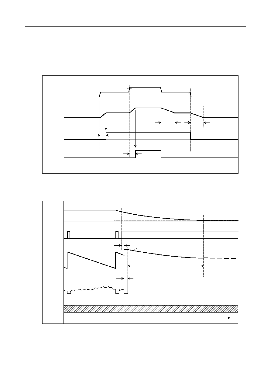
SDA 9380 - B21
Preliminary Data Sheet
Waveforms
Micronas
11-57
2001-05-03
11 Waveforms
11.1 Timing diagram of H35K and H38K
11.2 Black Switch-Off diagrams
H35K
H38K
f at
HSYNC
31 kHz
35 kHz
35 kHz
31 kHz
38 kHz
*) new H-frequency detected
H
f at HD
31 kHz
35 kHz
35 kHz
31 kHz
38 kHz
H
f
TH1
f
TH3
f
TH4
f
TH2
*)
*)
*)
*)
**)
**)
**) depends on decrease of B+
D1
t
D3
t
BSOIN
V
TH
VD+
HD
ca. 20% V
TH
t
D1
BSOIN controls VD+, VD- in mode 2, 3
continuously HD pulses until Power-On-Reset is going High
VBL com-
ponent of
SCP
ROUT,
BOUT,
GOUT
D2
t
overscan depends on selected BSO mode (s. next page)
t
D1
: 2...2.5 lines
t
D2
: 42 lines

SDA 9380 - B21
Preliminary Data Sheet
Waveforms
Micronas
11-58
2001-05-03
Mode 1 (constant overscan, BSO = 01):
Mode 2 (parabolic function, BSO = 10):
Mode 3 (linear function, BSO = 11):
0
10
20
30
40
50
60
70
80
90
100
80
88
96
104
112
120
128
136
144
152
160
V-overscan = f (voltage at BSOIN)
voltage BSOIN in %
V
-
ove
rs
c
a
n
i
n
%
V-overscan in %:
f 100
(
)
115
f 75
(
)
115
f 50
(
)
115
f 25
(
)
115
0
10
20
30
40
50
60
70
80
90
100
60
68
76
84
92
100
108
116
124
132
140
V-overscan = f (voltage at BSOIN)
voltage BSOIN in %
V-
o
v
e
r
s
can
in
%
V-overscan in %:
f 100
(
)
120.7
f 75
(
)
111.1
f 50
(
)
99.6
f 25
(
)
86
0
10
20
30
40
50
60
70
80
90
100
40
48
56
64
72
80
88
96
104
112
120
V-overscan = f (voltage at BSOIN)
voltage BSOIN in %
V-
o
v
e
r
s
can
in
%
V-overscan in %:
f 100
(
)
116.5
f 75
(
)
98.8
f 50
(
)
81
f 25
(
)
63

SDA 9380 - B21
Preliminary Data Sheet
Waveforms
Micronas
11-59
2001-05-03
11.3 Power On/Off diagram
Supply
Voltage
power on
Power-
On-
Reset
power off
X1, X2
HD
ready
I C-Bus
2
tristate
tristate
tri-
state
VREFH
Protection
inactive
active
de-
fault
de-
fault
de-
fault
CLL
32768
cycles
32768
cycles
SSD=0: ~ 8 lines
SSD=1: ~12 lines
inactive
active
CPU
max. 2.6V
~ 42 cycles
glitch
IIC registers 01..1C
programmable
IIC registers 01..1C
programmable
SSD=0: ~ 8 lines
SSD=1: ~12 lines
I
2
C-Reg.
01..1C
default
de-
fault
I
2
C-Reg.
00, 1D..30h
default
programmable
programmable
(HPROT
>1.5V)
programmable
programmable
ready
min. 1.5V
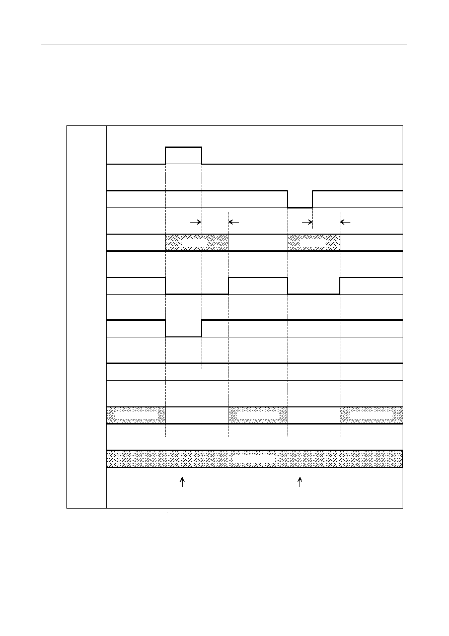
SDA 9380 - B21
Preliminary Data Sheet
Waveforms
Micronas
11-60
2001-05-03
11.4 Standby mode, RESN diagram
Standby
Standby mode
RESN
ext. reset
Protection
(HPROT
>1.5V)
inactive
active
I
2
C-Reg.
01..1C
~ 42 CLL
cycles
inactive
active
CPU
HD
Phi2-loop
free run
Phi2-loop
free run
Phi2-loop
VREFH
active
inactive
default values
programmable
default values
00, 1D..30h
~ 42 CLL
cycles
programmable
programmable
programmable
I
2
C-Reg.
SDA 9380 - B21
Preliminary Data Sheet
Waveforms
Micronas
11-61
2001-05-03
11.5 Function of H,V protection
HPROT
VPROT
Mode
SCP
HPON
VPON
b)
(IIC-Bus)
V1
V2
1
0
or
V2
6
t
0
< t < t
1
or
t > t
1
H, V in
operation
a)
a) depends on IIC control items
b) HPON = 1 or VPON = 1: HD = 1(off)
t
0
= 2/f
v
...3/f
v
t
1
= 64/f
v
...128/f
v
t
2
= 1/f
v
...2/f
v
continuous
blanking
b)
EHT
short over-
voltage
(IIC-Bus)
0
0
0
5
4
3
2
continuous
blanking
after t
2
1
after t
2
1
after t
1
1
after t
1
0
continuous
blanking
after t
0
if SSC = 0
continuous
blanking
after t
0
if SSC = 0
0
0
0
1
after t
2
continuous
blanking
after t
2
EHT over-
voltage
H off
after t
1
V short
failure
V longer
failure
H in
operation
or
or
or
t > t
1
or
start up
V1

SDA 9380 - B21
Preliminary Data Sheet
Waveforms
Micronas
11-62
2001-05-03
11.6 Black Stretch diagram
11.7 Soft Clipping diagram
50
100
0
100
50
Ou
t
p
u
t
(I
R
E
)
Input (IRE)
-30
maximum black stretch
0
1V
2V
0
O
u
t
put
Input
(R
,
G,
B
v
o
lt
age m
eas
ur
ed at
t
he out
put
r
e
l
a
t
i
v
e
t
o
c
u
t
-
of
f
at
nom
i
nal w
h
it
e dr
iv
e)
3V
4V
5V
1V
2V
3V
4V
5V
A B
Slope: IIC
soft clipping,
bits B1, B0
-2
-1
0
+1
range

SDA 9380 - B21
Preliminary Data Sheet
Package outlines
Micronas
12-63
2001-05-03
12 Package outlines
P-MQFP-64

All information and data contained in this data sheet are without any
commitment, are not to be considered as an offer for conclusion of a
contract, nor shall they be construed as to create any liability. Any new
issue of this data sheet invalidates previous issues. Product availability
and delivery are exclusively subject to our respective order confirmation
form; the same applies to orders based on development samples deliv-
ered. By this publication, Micronas GmbH does not assume responsibil-
ity for patent infringements or other rights of third parties which may
result from its use.
Further, Micronas GmbH reserves the right to revise this publication and
to make changes to its content, at any time, without obligation to notify
any person or entity of such revisions or changes.
No part of this publication may be reproduced, photocopied, stored on a
retrieval system, or transmitted without the express written consent of
Micronas GmbH.
SDA 9380-B21
PRELIMINARY DATA SHEET
7
2 Micronas
Micronas GmbH
Hans-Bunte-Strasse 19
D-79108 Freiburg (Germany)
P.O. Box 840
D-79008 Freiburg (Germany)
Tel. +49-761-517-0
Fax +49-761-517-2174
E-mail: docservice@micronas.com
Internet: www.micronas.com
Printed in Germany
Order No. 6251-549-
2PD