 | –≠–ª–µ–∫—Ç—Ä–æ–Ω–Ω—ã–π –∫–æ–º–ø–æ–Ω–µ–Ω—Ç: 53267 | –°–∫–∞—á–∞—Ç—å:  PDF PDF  ZIP ZIP |

Micropac Industries cannot assume any responsibility for any circuits shown or represent that they are free from patent infringement.
Micropac reserves the right to make changes at any time in order to improve design and to supply the best product possible.
MICROPAC INDUSTRIES, INC.
MICROCIRCUITS DIVISION ∑ 905 E. Walnut Street, Garland, TX 75040 ∑ (972) 272-3571 ∑ Fax (972) 494-2281
ww.micropac.com
E-MAIL: microsales@micropac.com 11/22/2002
PRELIMINARY DATA SHEET
53267
SOLID STATE RELAY, 80VDC-200mA,
LATCHING, SPST, with STATUS OUPUT
Mii
MICROCIRCUITS DIVISION
Features:
∑ High Voltage Optical Isolation Barrier
∑ Break-before-make Contact
∑ Latched Contact upon Removal of Power
∑ Extremely Low Power Control Input
∑ No Mechanical Moving Parts
Applications:
∑ Power Distribution In Land/Air/Launch Vehicles
∑ Motor/Solenoid Drivers
∑ Displays/Lamps Controls
∑ Industrial Automation
∑ Medical Lab Equipment
DESCRIPTION
The 53267 latching solid state relay (SSR) has no mechanical contact therefore it is immune to contact-related problems
(such as arcing, contamination, cycle life, etc.) associated with its electromechanical equivalent. Input/output isolation
barrier of the device is provided using optocoupler as shown in the functional block diagram (Figure 1). The control input
has a built-in current limiting resistor making it possible to directly interface to TTL logic signal. The contact uses a N-
channel enhancement mode MOSFET for low on-state resistance and is configured as a low-side switch. This results in
low power dissipation, which allows operation over the temperature range of ≠55∞C to +125∞C with minimal heat sinking.
In the absence of its bias voltage, the switch is default to the high impedance (off) state, i.e., open contact mode.
The control circuitry of the device is designed in a manner that the MOSFET turns completely off before it will turn on
emulating the break-before-make feature of the equivalent mechanical contact. Contact is toggled by applying a short
pulse at the control input resulting in very low average power dissipation and suitable for computer control applications.
The proprietary design of the solid state contact provides a "memory" capability for latching on (close) or off (open)
without reset upon removal of power.
The MOSFET switch in the device operates as a SPST. There is a status line available the monitoring the contact
position. The status output is an open collector signal will require an appropriate external pull-up resistor for it to works
properly. The device is encased in a hermetically sealed 10-pin TO-5 metal package. This SSR is available in a variety of
quality levels from COTS to class K including any custom screening requirements. The basic data sheet part is
environmentally screened to H level in accordance with Table C-IX of MIL-PRF-38534.
ABSOLUTE MAXIMUM RATINGS
(@ T
C
= 25∞C unless otherwise specified)
Input Control Current......................................................................................................................................................20 mA
Reverse Input Voltage (Control to Signal Ground)..................................................................................................... - 5 VDC
Control Bias Voltage ................................................................................................................................................... 6 VDC
Status Supply Voltage ............................................................................................................................................... 40 VDC
Output Blocking Voltage ............................................................................................................................................ 80 VDC
Pins to Case Isolation.................................................................................................................................................500 VDC
Input-Output Isolation .............................................................................................................................................. 1000 VDC
Lead Temperature (15 seconds) ................................................................................................................................. +300∞C
Junction Temperature .................................................................................................................................................. +150∞C

Micropac Industries cannot assume any responsibility for any circuits shown or represent that they are free from patent infringement.
Micropac reserves the right to make changes at any time in order to improve design and to supply the best product possible.
MICROPAC INDUSTRIES, INC.
MICROCIRCUITS DIVISION ∑ 905 E. Walnut Street, Garland, TX 75040 ∑ (972) 272-3571 ∑ Fax (972) 494-2281
ww.micropac.com
E-MAIL: microsales@micropac.com 11/22/2002
53267
80VDC-200mA LATCHING
SOLID STATE RELAY with STATUS OUTPUT
SPECIFICATIONS
(@ T
C
= 25∞C unless otherwise specified)
Control Input
Type .................................................................................................................................................................................. LED
Control Pulse Amplitude..................................................................................................................................... 5 VDC ± 10%
Control Pulse Current..............................................................................................................................................2 mA (min)
Control Pulse Width............................................................................................................................................... 10 ms (min)
Bias Supply
Bias Voltage........................................................................................................................................................ 5 VDC ± 10%
Bias Current......................................................................................................................................................................8 mA
Power Output (Contact)
Load Voltage ................................................................................................................................................................80 VDC
Output Leakage Current................................................................................................................................................250
µA
Continuous Current ......................................................................................................................................................200 mA
On-state Resistance, T
j
@ 25∞C................................................................................................................................. 600 m
On-state Resistance, T
j
@ 150∞C............................................................................................................................. 1300 m
Status Output (Open Collector)
Supply Voltage, V
CC
.......................................................................................................................................... 30 VDC (max)
High-level Output Voltage, V
OH
...........................................................................................................................................V
CC
Low-level Output Voltage, V
OL
......................................................................................................................... 0.4 VDC (max)
Temperature Ranges
Operating (Case), T
C
..................................................................................................................................... -55∞C to +125∞C
Storage .......................................................................................................................................................... -55∞C to +150∞C
Thermal Resistance
Junction to Case...................................................................................................................................................... TBD ∞C/W
Physical Characteristics
Dimensions ....................................................................................................... see Figure 4 - Package Dimensional Outline
Weight.....................................................................................................................................................................TBD grams
Power Output and Status Switching Characteristics
Turn-on Time, t
ON
(see Figure 3) ........................................................................................................................... 6 ms (max)
Turn-off Time, t
OFF
(see Figure 3)........................................................................................................................... 3 ms (max)
Bias Reset Delay Time, t
RESET
(see Figure 2) ...................................................................................................... 10 ms (max)
Micropac Industries cannot assume any responsibility for any circuits shown or represent that they are free from patent infringement.
Micropac reserves the right to make changes at any time in order to improve design and to supply the best product possible.
MICROPAC INDUSTRIES, INC.
MICROCIRCUITS DIVISION ∑ 905 E. Walnut Street, Garland, TX 75040 ∑ (972) 272-3571 ∑ Fax (972) 494-2281
ww.micropac.com
E-MAIL: microsales@micropac.com 11/22/2002
53267
80VDC-200mA LATCHING
SOLID STATE RELAY with STATUS OUTPUT
+ 5VDC BIAS
+ OUT
STATUS
(OPEN COLLECTOR)
COMMON
LOGIC
CONTROL
SOLID
STATE
LATCH
CNTL_IN
CNTL_RTN
GATE
DRIVE
CIRCUIT
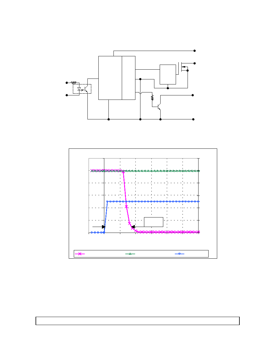
Figure 1 ≠ Functional Block Diagram
Figure 2 ≠ Typical Bias Reset Delay Time
0.0
0.2
0.4
0.6
0.8
1.0
1.2
-5
0
5
10
15
20
25
30
Time, milliseconds
N
o
r
m
al
i
z
ed C
ont
ac
t
B
u
s
V
o
l
t
age
0
2
4
6
8
10
12
Bi
a
s
Vo
l
t
a
g
e
,
VD
C
Close Contact Voltage
Open Contact Voltage
Bias Voltage
t
RESET

Micropac Industries cannot assume any responsibility for any circuits shown or represent that they are free from patent infringement.
Micropac reserves the right to make changes at any time in order to improve design and to supply the best product possible.
MICROPAC INDUSTRIES, INC.
MICROCIRCUITS DIVISION ∑ 905 E. Walnut Street, Garland, TX 75040 ∑ (972) 272-3571 ∑ Fax (972) 494-2281
ww.micropac.com
E-MAIL: microsales@micropac.com 11/22/2002
53267
80VDC-200mA LATCHING
SOLID STATE RELAY with STATUS OUTPUT
Figure 3 ≠ Typical Switching Characteristics
.017
-.001
+.002
DIA.
.200±.010 DIA.
10
1
2
3
4
5
6
7
8
9
Figure 4 ≠ Package Dimensional Outline
0.0
0.2
0.4
0.6
0.8
1.0
1.2
-2
0
2
4
6
8
10
12
14
16
Time, milliseconds
Nor
m
a
liz
ed Cont
ac
t
B
u
s
V
o
lt
age
0
0.4
0.8
1.2
1.6
2
2.4
Cont
r
o
l I
nput
,
V
D
C
Close Contact
Open Contact
Control Input
t
ON
t
OFF
Micropac Industries cannot assume any responsibility for any circuits shown or represent that they are free from patent infringement.
Micropac reserves the right to make changes at any time in order to improve design and to supply the best product possible.
MICROPAC INDUSTRIES, INC.
MICROCIRCUITS DIVISION ∑ 905 E. Walnut Street, Garland, TX 75040 ∑ (972) 272-3571 ∑ Fax (972) 494-2281
ww.micropac.com
E-MAIL: microsales@micropac.com 11/22/2002
53267
80VDC-200mA LATCHING
SOLID STATE RELAY with STATUS OUTPUT
Pin
number
Function
1 STATUS
2 NC
(1)
3 CNTL_RTN
4 CNTL_IN
5 COMMON
6 NC
(1)
7 +
OUT
8 +5VDC
BIAS
9 NC
(1)
10 NC
(1)
Note: (1) Pins 2, 6, 9, and 10 are for internal interconnection only. Apply any potential to these
pins will cause permanent damage to the hybrid.
Figure 5 ≠ Tentative Pin Assignment
Control Bias
Contact
position
Status
pulse ON
CLOSE
(ON)
LOW
pulse ON
OPEN
(Off)
HIGH
Don't care
OFF
OPEN (Off)
HIGH
Figure 6 ≠ Truth Table