
MICROPAC INDUSTRIES, INC.
OPTOELECTRONIC PRODUCTS DIVISION ∑ 725 E. Walnut St., Garland, TX 75040 ∑ (972) 272-3571 ∑ Fax (972) 487-6918
www.micropac.com
E-MAIL: optosales@micropac.com
3 - 36
66058
SINGLE/DUAL CHANNEL, LOW-INPUT CURRENT,
OPTOCOUPLER (Electrically similar to 6N140)
Mii
OPTOELECTRONIC PRODUCTS
DIVISION
Features:
∑ DSCC Approved 8978501PX (Dual) and
8981001PX (Single)
∑ High current transfer ratio: 1000% typical
∑ 1500 Vdc isolation test voltage
∑ Low input current requirement: 0.5mA
Applications:
∑ Telephone ring detection
∑ Voltage
level
shifting
∑ Isolated receiver input
∑ Communication
systems
∑ Medical
systems
DESCRIPTION
The 66058 single/dual optocoupler utilizes infrared LEDs optically coupled to high gain photodarlington detectors. This unique
optocoupler provides high CTR and low leakage current over the full military temperature range (-55
∞
to +125∞C). The 66058
is a 8 pin dual-in-line, hermetically sealed package and is available in standard and screened versions or tested to customer
specifications.
ABSOLUTE MAXIMUM RATINGS
Storage Temperature........................................................................................................................................... -65∞C to +150∞C
Operating Free-Air Temperature Range ............................................................................................................. -55∞C to +125∞C
Lead Solder Temperature.........................................................................................260
∞
C for 10s (1.6mm below seating plane)
Peak Forward Input Current (each channel) ................................................................................................ 20mA (1ms duration)
Average Forward Input Current .......................................(see Note 1) ...............................................................................10mA
Reverse Input Voltage ...............................................................................................................................................................5V
Output Current - I
O
(each channel) ......................................................................................................................................40mA
Output Power Dissipation (each channel) ........................(see Note 2) ..............................................................................50mW
Supply Voltage - V
CC
..........................................................(see Note 3)........................................................................0.5 to 20V
Output Voltage - V
O
(each channel)...............................(see Note 3) ...................................................................... -0.5 to 20V
Package Dimensions Schematic Diagram
ALL DIMENSIONS ARE IN INCHES [MILLIMETERS]
SIDE VIEW
REAR VIEW
2
4
3
1
YYWW
XXXX
USA
END VIEW
6
8
7
5
0.170 [4.32]MAX
.020 [0.51] MAX
0.90 [2.28]
0.110 [2.80]
PIN ONE
TYPE NUMBER
0.370 [9.040]
0.390 [9.90]
0.007 [0.18]
0.013 [0.33]
0.320 [8.13]MAX
DATE CODE
0.280 [7.11]
0.310 [7.88]
1
2
4
3
8
7
6
5 GND
V0
EN
Vcc
K
NC
A
NC
K 3
4
A
2
K
A 1
GND
5
6 V02
7 V01
Vcc
8
PIN ONE
0.020 [0.51] MIN
Notes:
1. Derate
I
F
at 0.33 mA/
∞
C above 110∞C.
2. Collector output power plus one half of the total supply power is total output power. Derate at 1.66mW/∞C above 110∞C.
3. The lowest total I
OH
over temperature is developed by keeping V
CC
as low as possible, but greater that 2 volts. The
negative voltage at the detector side should be applied to Pin 10.
MICROPAC INDUSTRIES, INC.
OPTOELECTRONIC PRODUCTS DIVISION ∑ 725 E. Walnut St., Garland, TX 75040 ∑ (972) 272-3571 ∑ Fax (972) 487-6918
www.micropac.com
E-MAIL: optosales@micropac.com
3 - 37
66058
SINGLE/DUAL CHANNEL, LOW-INPUT CURRENT OPTOCOUPLER
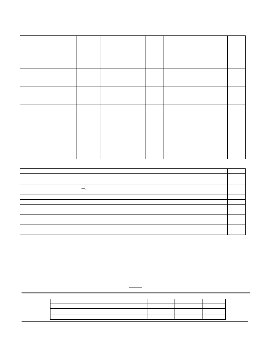
ELECTRICAL CHARACTERISTICS
T
a
= -55
∞
C to 125
∞
C unless otherwise specified.
PARAMETER
SYMBOL
MIN
TYP
MAX
UNITS
TEST CONDITIONS
NOTE
Current Transfer Ratio
CTR
300
300
200
1000
750
400
%
%
%
I
F
= 0.5mA, V
O
= 0.4V, V
CC
= 4.5V
I
F
= 1.6mA, V
O
= 0.4V, V
CC
= 4.5V
I
F
= 5.0mA, V
O
= 0.4V, V
CC
= 4.5V
1,2
1,2
1,2
Logic Low Output Voltage
V
OL
0.1
0.2
0.4
0.4
V
V
I
F
= 0.5mA, I
OL
= 1.5mA, V
CC
= 4.5V
I
F
= 5.0mA, I
OL
= 10mA, V
CC
= 4.5V
1
Logic High Output Current
I
OH
.005
250
µ
A
I
F
= 2
µ
A, V
O
= V
CC
= 18V
1,3
High Level Output Current -XX1
-XX2
I
CCH
.01
10
20
µ
A
µ
A
I
F1
= 0mA, V
CC
= 18V
I
F1
= I
F2
= 0mA, V
CC
= 18V
Low Level Supply Current -XX1
-XX2
I
CCL
.01
2
4
mA
mA
I
F1
= 1.6mA, V
CC
= 18V
I
F1
= I
F2
=1.6mA, V
CC
= 18V
Input Forward Voltage
V
F
1.4
1.7
V
I
F
= 1.6mA
1
Input Reverse Breakdown Voltage
BV
R
5
V
I
R
= 10µA
1
Input-Output Insulation Leakage
Current
I
I--O
1.0
µA
V
I--0
= 1500Vdc,
Relative Humidity = 45%
t
A
= 25∞C, t = 5s
4
Propagation Delay Time To High
Output Level
t
PLH
6
6
4
60
50
30
µ
s
µ
s
µ
s
I
F
= 0.5mA, V
CC
= 5.0V, R
L
= 4.7k
I
F
= 1.6mA, V
CC
= 5.0V, R
L
= 1.5k
I
F
= 5mA, V
CC
= 5.0V, R
L
= 680
Propagation Delay Time To Low
Output Level
t
PHL
8
3
2
100
30
10
µ
s
µ
s
µ
s
I
F
= 0.5mA, V
CC
= 5.0V, R
L
= 4.7k
I
F
= 1.6mA, V
CC
= 5.0V, R
L
= 1.5k
I
F
= 5mA, V
CC
= 5.0V, R
L
= 680
TYPICAL CHARACTERISTICS
T
a
= 25
∞
C, V
CC
= 5V Each Channel
PARAMETER
SYMBOL
MIN
TYP
MAX
UNITS
TEST CONDITIONS
NOTE
Input Capacitance
C
IN
60
pF
V
F
= 0, f = MHz, t
a
= 25∞C
1
Capacitance (Input-Output)
C
I-O
1.5
pF
f = 1MHz, t
a
= 25
∞
C
1, 5
Input Diode Temperature
Coefficient
v
F
T
A
-1.8
mV/
∞
C
I
F
= 1.6mA
1
Resistance (Input-Output)
R
I-0
10
12
V
I--O
= 500V, t
a
= 25
∞
C
1, 5
Resistance (Input-Input)
R
I-I
10
12
V
I--I
= 500V, t
a
= 25
∞
C
6
Input-Input Insulation Leakage
Current
I
I-I
0.5
nA
Relative Humidity = 45%
V
I--I
= 500V, t = 5s
6
Common Mode Transient
immunity at High Output Level
CM
H
500
1000
V/
µ
s
V
CM
= 50V
P-P
,V
CC
= 5.0V,
R
L
= 1.5k
, I
F
= OmA, t
a
= 25
∞
C
7,9
Common Mode Transient
Immunity at Low Output Level
CM
L
500
1000
V/
µ
s
V
CM
= 50V
P-P
,V
CC
= 5.0V,
R
L
= 1.5k
, I
F
= 1.6mA, t
a
= 25
∞
C
8,9
NOTES:
1. Each
channel.
2.
CURRENT TRANSFER RATIO is defined as the ratio of output collector current, I
O
, to the forward LED input current., I
F
, times 100%.
3. I
F
= 2
µ
A for channel under test. For all other channels, I
F
= 10mA.
4.
Device considered a two-terminal device.
5.
Measured between each input pair shorted together and all output pins shorted together.
6.
Measured between each input pair shorted together.
7. CM
H
is the maximum tolerable common mode transient to assure that the output will remain in a high logic state (ie. V
O
>
@.0V).
8. CM
L
is the maximum tolerable common mode transient to assure that the output will remain in a low logic state (ie. V
O
<
0.8V).
9.
In applications where dv/dt may exceed 50,000 V/
µ
s (such as static discharge) a series resistor, R
CC
, should be included to protect the detector IC's from
destructively high surge currents. The recommended value is R
CC
= 1V = k
0.6I
F
(mA)
RECOMMENDED OPERATING CONDITIONS:
PARAMETER
SYMBOL
MIN
MAX
UNITS
Input Current, Low Level
I
FL
0
2
µ
A
Input Current, High Level
I
FH
0.5
5
mA
Supply Voltage
V
CC
2.0
18
V