MICROPAC INDUSTRIES, INC.
OPTOELECTRONIC PRODUCTS DIVISION ∑ 725 E. Walnut St., Garland, TX 75040 ∑ (972) 272-3571 ∑ Fax (972) 487-6918
www.micropac.com
E-MAIL: optosales@micropac.com
3 - 40
66088
SINGLE/DUAL, HIGH SPEED OPTOCOUPLER
Mii
OPTOELECTRONIC PRODUCTS
DIVISION
Features:
∑ Electrically similar to 4N55
∑ 1500 Vdc isolation test voltage
∑ Low
power
consumption
∑ 2 MHz bandwidth typical
∑ Low output saturation voltage
Applications:
∑ Digital logic ground isolation
∑ Microprocessor system interface
∑ Isolated receiver input
∑ Communication
systems
∑ Medical
systems
DESCRIPTION
The 66088 single/dual optocouplers utilize infrared LEDs optically coupled to high gain photon detectors. These unique
optocouplers provide high CTR and low leakage current. The 66088 optocouplers are available in military temperature range
and military temperature with 100% device screening. The devices are built in an 8 pin hermetic, side-brazed package and
provide high input to output isolation (1500Vdc minimum).
ABSOLUTE MAXIMUM RATINGS
Storage Temperature........................................................................................................................................... -65∞C to +150∞C
Operating Free-Air Temperature Range ............................................................................................................. -55∞C to +125∞C
Lead Solder Temperature.........................................................................................260
∞
C for 10s (1.6mm below seating plane)
Peak Forward Input Current (per channel)................................................................................................... 40mA (1ms duration)
Average Forward Input Current (per channel)...........(see Note 2) ......................................................................................20mA
Reverse Input Voltage (each channel) ......................................................................................................................................5V
Supply Voltage - V
CC
. (each channel)...............................(see Note 1) .......................................................... -0.5 to 20V Output
Output Current - I
O
(each channel) ........................................................................................................................................8mA
Output Power Dissipation (each channel)...(derate linearly at a rate of 1.4mW/∫C above 100∫C) ....................................50mW
Output Voltage - V
O
(each channel)...............................(see Note 1) ...................................................................... -0.5 to 20V
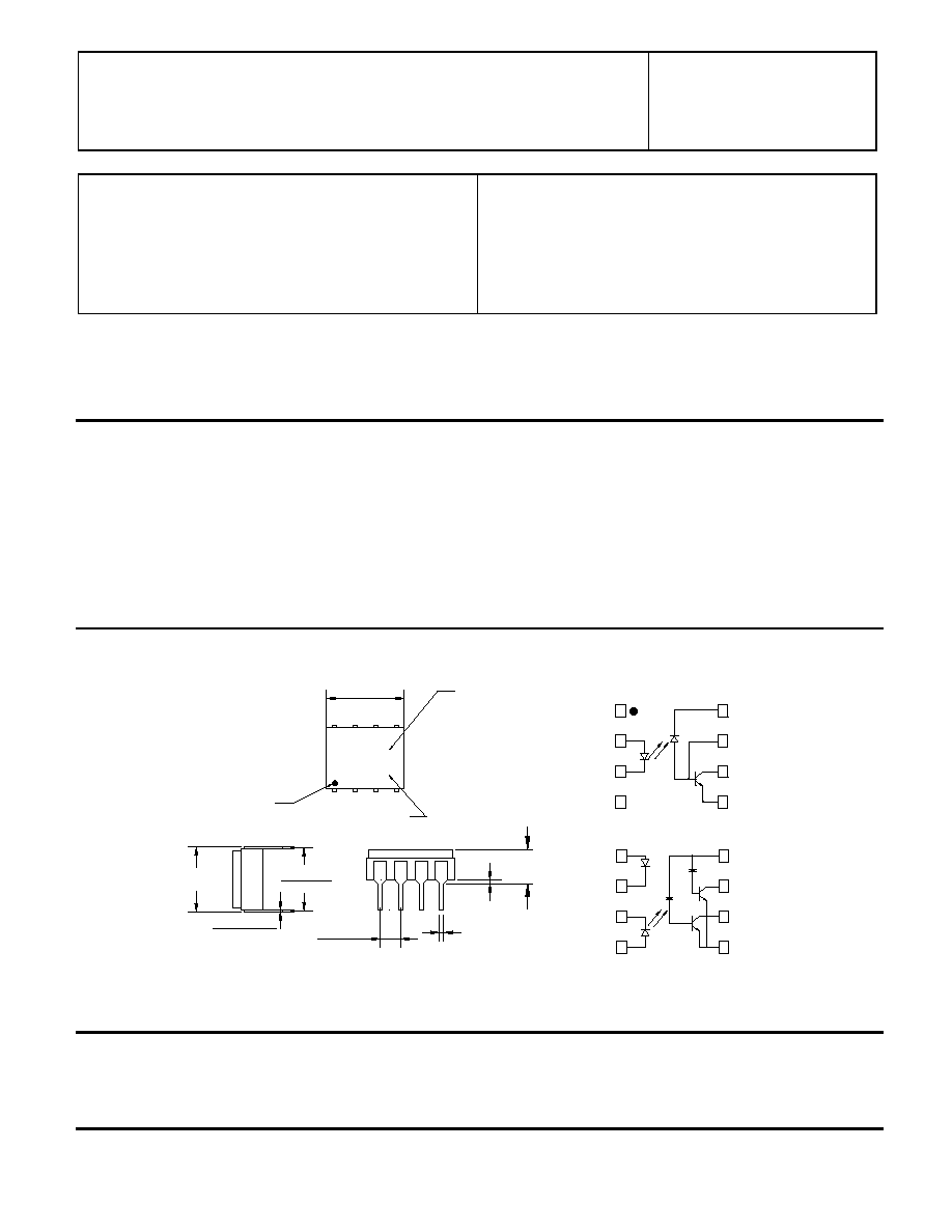
Package Dimensions Schematic Diagram
ALL DIMENSIONS ARE IN INCHES [MILLIMETERS]
NOTE:
SIDE VIEW
REAR VIEW
2
4
3
1
YYWW
XXXX
USA
END VIEW
6
8
7
5
0.170 [4.32]MAX
.020 [0.51] MAX
0.90 [2.28]
0.110 [2.80]
PIN ONE
TYPE NUMBER
0.370 [9.040]
0.390 [9.90]
0.007 [0.18]
0.013 [0.33]
0.320 [8.13]MAX
DATE CODE
0.280 [7.11]
0.310 [7.88]
1
2
4
3
8
7
6
5 GND
V0
EN
Vcc
K
NC
NC
K 3
4
A
2
K
A 1
GND
5
6 V02
7 V01
Vcc
8
PIN ONE
0.020 [0.51] MIN
A
Notes:
1. The lowest total I
OH
over temperature is developed by keeping V
CC
as low as possible, but greater than 2V. The negative
voltage at the detector side should be applied to PIN 5.
2. Derate
I
F
at 0.1 mA/
∫
C above 25∞C.
MICROPAC INDUSTRIES, INC.
OPTOELECTRONIC PRODUCTS DIVISION ∑ 725 E. Walnut St., Garland, TX 75040 ∑ (972) 272-3571 ∑ Fax (972) 487-6918
www.micropac.com
E-MAIL: optosales@micropac.com
3 - 41
66088
SINGLE/DUAL CHANNEL, HIGH SPEED OPTOCOUPLER
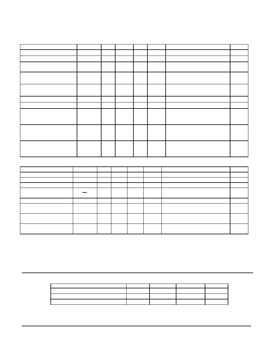
ELECTRICAL CHARACTERISTICS
T
a
= -55
∞
C to 125
∞
C unless otherwise specified.
PARAMETER
SYMBOL
MIN
TYP
MAX
UNITS
TEST CONDITIONS
NOTE
Current Transfer Ratio
CTR
9
24
%
I
F
= 16mA, V
O
= 0.4V, V
CC
= 4.5V
1,2
Logic Low Output Voltage
V
OL
0.1
0.4
V
I
F
= 16mA, I
OL
= 2.4mA, V
CC
= 4.5V
Logic High Output Current
I
OH
20
100
µ
A
I
F
= 0, V
CC
= V
O
= 15V
I
F
(other channel)
= 16mA
1
High Level Output Current
I
CCH
0.1
20
µ
A
I
F
= V
CC
= 15V
I
F
(other channel)
= 0mA
1
Low Level Supply Current
I
CCL
2
mA
I
F1
= 16mA, V
CC
= 15V
I
F
(other channel)
= 16mA
1
Input Forward Voltage
V
F
1.5
1.8
V
I
F
= 16mA
1
Input Reverse Breakdown Voltage
BV
R
5
V
I
R
= 10µA
1
Input-Output Insulation Leakage
Current
I
I--O
1.0
µA
V
I--0
= 1500Vdc,
Relative Humidity = 45%
t
A
= 25∞C, t = 5s
3
Propagation Delay Time To High
Output Level
t
PLH
.08
1.6
µ
s
I
F
= 16mA, V
CC
= 5V, R
L
= 1.9k
1
Propagation Delay Time To Low
Output Level
t
PHL
.08
1.6
µ
s
I
F
= 16mA, V
CC
= 5V, R
L
= 1.9k
1
TYPICAL CHARACTERISTICS
T
a
= 25
∞
C, V
CC
= 5V Each Channel
PARAMETER
SYMBOL
MIN
TYP
MAX
UNITS
TEST CONDITIONS
NOTE
Input Capacitance
C
IN
60
pF
V
F
= 0, f = MHz
1
Capacitance (Input-Output)
C
I-O
1.5
pF
f = 1MHz, V
F
= 0
1, 4
Capacitance (Input-Output)
C
I-l
0.55
pF
f = 1MHz
Input Diode Temperature
Coefficient
v
F
T
A
-1.8
mV/
∞
C
I
F
= 16mA
1
Resistance (Input-Output)
R
I-0
10
12
V
I--0
= 500Vdc
1
Input-Input Insulation Leakage
Current
I
I-l
0.5
nA
Relative Humidity = 45%
V
I--I
= 500Vdc, t = 5s
3
Common Mode Transient
immunity at High Output Level
CM
H
500
1000
V/
µ
s
V
CM
= 10V
P-P
,
R
L
= 1.9k
, I
F
= OmA
1, 5
Common Mode Transient
Immunity at Low Output Level
CM
L
500
1000
V/
µ
s
V
CM
= 10V
P-P
,
R
L
= 1.9k
, I
F
= 16mA
1, 6
NOTES:
1. Each
channel.
2.
CURRENT TRANSFER RATIO is defined as the ratio of output collector current, I
O
, to the forward LED input current., I
F
, times 100%.
3.
Measured between each input pair shorted together.
4.
Measured between input pins shorted together and the output pins for that channel shorted together.
5. CM
H
is the maximum tolerable common mode transient to assure that the output will remain in a high logic state (ie. V
O
>
2.0V).
6. CM
L
is the maximum tolerable common mode transient to assure that the output will remain in a low logic state (ie. V
O
<
0.8V).
RECOMMENDED OPERATING CONDITIONS:
PARAMETER
SYMBOL
MIN
MAX
UNITS
Input Current, Low Level (each channel)
I
FL
0
2
µ
A
Input Current, High Level (each channel)
I
FH
16
20
mA
Supply Voltage
V
CC
2.0
18
V