MICROPAC INDUSTRIES, INC.
OPTOELECTRONIC PRODUCTS DIVISION ∑ 725 E. Walnut St., Garland, TX 75040 ∑ (972) 272-3571 ∑ Fax (972) 487-6918
www.micropac.com
E-MAIL: optosales@micropac.com
5 - 8
66095
MINIATURE LCC OPTOCOUPLER
Mii
OPTOELECTRONIC PRODUCTS
DIVISION
Features:
∑ Electrically similar to 4N47, 4N48, or 4N49
∑ Standard and screened versions available
∑ Hermetically sealed 4 pin LCC
∑ High-voltage electrical isolation...1kV rating
Applications:
∑ High density surface mount circuits
∑ Ground loop isolation
∑ Feedback
controls
∑ General purpose switching circuits
DESCRIPTION
The 66095 series optocouplers consist of an infrared LED and a silicon phototransistor in a 4 pin hermetically sealed
leadless chip carrier. The 66095 is electrically similar to the 4N47, 4N48, or 4N49 series optocouplers, and is available in
standard and screened versions. The 66095 miniature LCC is ideal for surface mount applications where board space is
limited.
ABSOLUTE MAXIMUM RATINGS
Input-to-Output Voltage ......................................................................................................................................................± 1 KV
Collector-Emitter Voltage.......................................................................................................................................................40 V
(This value applies with the input-diode current equal to zero)
Input Diode Reverse Voltage................................................................................................................................................... 2 V
Input Diode Continuous Forward Current at (or below) 65
∞
C Free-Air Temperature........................................................40 mA
(Derate linearly to 125∞C free-air temperature at the rate of 0.67 mA/
∞
C)
Continuous Collector Current ............................................................................................................................................50 mA
Peak Diode Current.....(This Value applies for tw
<
1
µ
s, PRR
<
300 pps).............................................................................. 1A
Continuous Transistor Power Dissipation at (or below) 25
∞
C Free-Air Temperature .....................................................300mW
(Derate linearly to 125∞C free-air temperature at the rate of 3 mW/
∞
C)
Operating and Storage Free-Air Temperature Range .......................................................................................-55
∞
C to +125
∞
C
Lead Temperature 1.6mm (1/16 inch) from Case for 10 seconds..................................................................................... 245
∞
C
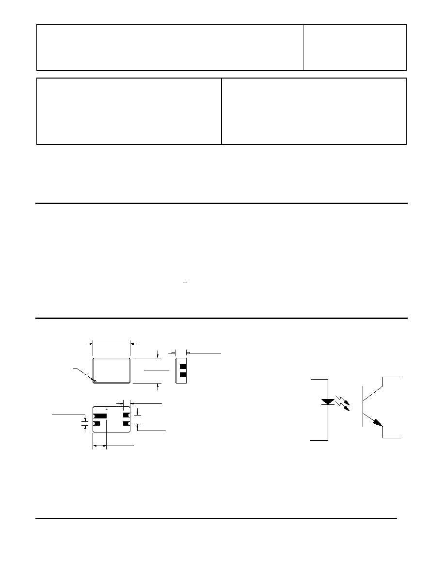
Package Dimensions
Schematic Diagram
K
A
C
E
1
2
3
4
ALL DIMENSIONS ARE IN INCHES [MILLIMETERS]
1
4
2
3
IDENTIFIER
PIN 1
0.215 [5.46]
0.145 [3.68]
0.155 [1.40]
0.061 [1.55]
0.075 [1.91]
0.032 [0.81]
3 PL
0.045 [1.14]
0.072 [1.83]
0.022 [0.56]
0.028 [0.17]
0.088 [2.24]
0.055 [1.40]
0.225 [5.72]
0.048 [1.22]

MICROPAC INDUSTRIES, INC.
OPTOELECTRONIC PRODUCTS DIVISION ∑ 725 E. Walnut St., Garland, TX 75040 ∑ (972) 272-3571 ∑ Fax (972) 487-6918
www.micropac.com
E-MAIL: optosales@micropac.com
5 - 9
66095
MINATURE LCC OPTOCOUPLER, Continued
ELECTRICAL CHARACTERISTICS
T
A
= 25
∞C unless otherwise specified.
PARAMETER
SYMBOL
MIN
TYP
MAX
UNITS
TEST CONDITIONS
NOTE
Input Diode Static Reverse Current
I
R
100
µA
V
R
= 2V
Input Diode Static Forward Voltage
-55
∞
C
+25
∞
C
+100
∞
C
V
F
1.3
1.3
1.3
1.5
1.5
1.5
1.7
1.7
1.7
V
V
V
I
F
= 10mA
OUTPUT TRANSISTOR
T
A
= 25
∞C unless otherwise specified.
Collector-Emitter Breakdown Voltage
V
(BR)CEO
40
V
I
C
= 1mA, I
F
= 0
COUPLED CHARACTERISTICS
T
A
= 25
∞C unless otherwise specified.
On State Collector Current
-XX1
T
a
= +25
∞
C
-XX2
-XX3
I
C(ON)
0.5
1
2
-
5
10
mA
V
CE
= 5V, I
F
= 1mA
On State Collector Current
-XX1
T
a
= -55
∞
C
-XX2
-XX3
I
C(ON)
0.7
1.4
2.8
mA
V
CE
= 5V, I
F
= 2mA
On State Collector Current
-XX1
T
a
= +100
∞
C
-XX2
-XX3
I
C(ON)
0.5
1.0
2.0
mA
V
CE
= 5V, I
F
= 2mA
2
Off State Collector Current
I
C(OFF)
100
nA
V
CE
= 20V, I
F
= 0mA
Off State Collector Current, T
a
= 100
∞
C
I
C(OFF)
100
µ
A
V
CE
= 20V, I
F
= 0mA
Collector-Emitter Saturation Voltage -X01
-X02
-X03
V
CE(SAT)
V
CE(SAT)
V
CE(SAT)
0.3
0.3
0.3
V
V
V
I
F
= 2mA, I
C
= 0.5mA
I
F
= 2mA, I
C
= 1mA
I
F
= 2mA, I
C
= 2mA
Input to Output Resistance
R
IO
10
11
V
IN-OUT
= 1kV
1
Input to Output Capacitance
C
IO
2.5
5
pF
F = 1MHz, V
IN-OUT
= 0
1
Rise Time (Phototransistor Operation)
-XX1
or
-XX2
Fall Time -XX3
t
r
or
t
f
10
10
10
20
25
25
µ
s
V
CC
= 10V, I
C
= 5mA,
R
L
= 100
NOTES:
1.
These parameters are measured between all phototransistor leads shorted together and with both input diode leads shorted together.
2.
This parameter must be measured using pulse techniques. t
w
= 100
µ
s, duty cycle
1%.
RECOMMENDED OPERATING CONDITIONS:
PARAMETER
SYMBOL
MIN
MAX
UNITS
Input Current, Low Level
I
FL
0
100
µ
A
Input Current, High Level
I
FH
1
2
mA
Supply Voltage
V
CC
5.0
20
V
Operating Temperature
T
A
-55
125
∞
C