MICROPAC INDUSTRIES, INC.
OPTOELECTRONIC PRODUCTS DIVISION ∑ 725 E. Walnut St., Garland, TX 75040 ∑ (972) 272-3571 ∑ Fax (972) 487-6918
www.micropac.com
E-MAIL:
optosales@micropac.com
3 - 18
66099
RADIATION TOLERANT OPTOCOUPLER
Mii
OPTOELECTRONIC PRODUCTS
DIVISION
Features:
∑ Meets or exceeds MIL-PRF-19500 radiation
requirements
∑ Current Transfer Ratio-150% typical
∑ 1kVdc electrical input to output isolation
∑ Base lead provided for conventional transistor
biasing
Applications:
∑ Eliminate ground loops
∑ Level shifting
∑ Line receiver
∑ Switching power supplies
∑ Motor control
DESCRIPTION
Radiation tests performed on the 66099 optocoupler have shown that the electrical performance of the device after irradiation
is an order of magnitude better that the 4N49 optocouplers. The 66099 Optocoupler consist of a GaAIA's LED optically
coupled to a photodiode detector circuit mounted in a hermetic TO-5 package. Figures 1 and 2 illustrate the radiation
performance of the device. Micropac's 66099 performs beyond the levels shown in MIL-PRF-19500 for a level H (total
dose>10
6
rads, neutron fluence >1X10
12
n/cm
2
) RHA designation.
ABSOLUTE MAXIMUM RATINGS
Storage Temperature..........................................................................................................................................-65∞C to +150∞C
Operating Free-Air Temperature Range ............................................................................................................-55∞C to +100∞C
Lead Solder Temperature (1/16" (1.6mm) from case for 10 seconds) ............................................................................. 240∞C
Input Diode Forward DC Current.........................................................................................................................................40mA
Input Power Dissipation (see Note 1) ...............................................................................................................................80mW
Reverse Input Voltage ............................................................................................................................................................. 3V
Collector-Base Voltage ...........................................................................................................................................................40V
Collector-Emitter Voltage .......................................................................................................................................................40V
Emitter-Base Voltage................................................................................................................................................................ 4V
Continuous Collector Current ..............................................................................................................................................50mA
Continuous Transistor Power Dissipation (see Note 2) ..................................................................................................300mW
Notes:
1. Derate linearly 0.80 mW/∞C above 25∞C.
2. Derate linearly 3.0 mW/∞C above 25∞C.
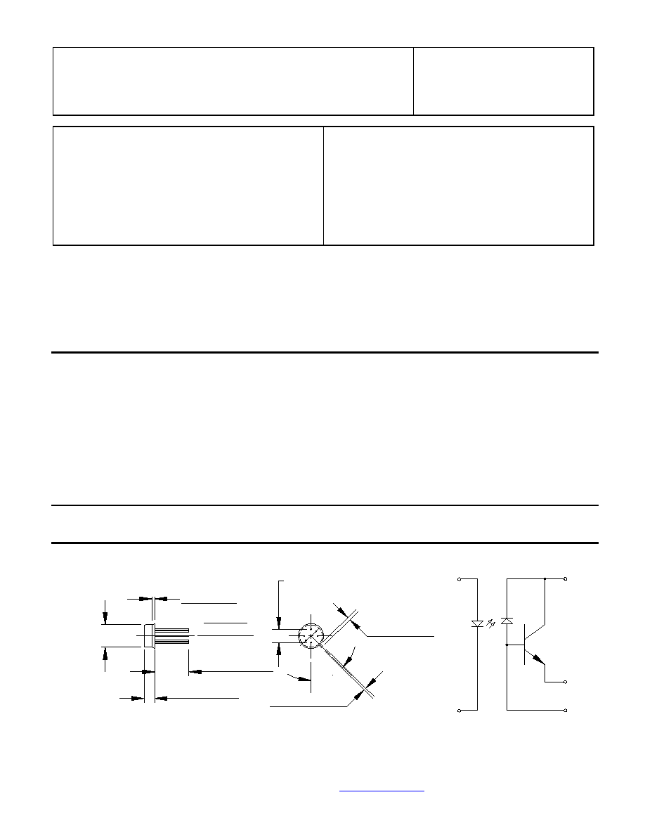
Package Dimensions Schematic Diagram
NOTE: ALL LINEAR DIMENSIONS ARE IN INCHES (MILLIMETERS)
6 LEADS
0.016ÿ [0.41]
0.019ÿ [0.48]
1
2
3
5
6
7
0.335 [8.51]
0.305 [7.75]
MIN.
0.040 [1.02]
MAX.
0.500 [12.70]
0.155 [3.94]
0.185 [4.70]
0.045 [1.14]
0.029 [0.73]
0.034 [0.864]
0.028 [0.711]
45∞
0.022ÿ [5.08]
5
7
3
1
2
B
E
C
66099

MICROPAC INDUSTRIES, INC.
OPTOELECTRONIC PRODUCTS DIVISION ∑ 725 E.Walnut St., Garland, TX 75040 ∑ (972) 272-3571 ∑ Fax (972) 487-6918
www.micropac.com
E-MAIL: optosales.com
3 - 19
INPUT DIODE CHARACTERISTICS
T
A
= 25
∞
C unless otherwise specified.
PARAMETER SYMBOL
MIN
TYP
MAX UNITS TEST
CONDITIONS
Input Diode Static Reverse Current
I
R
100 µA
V
R
= 2V
Input Diode Static Forward Voltage
V
F
0.8 2 V
I
F
= 10mA
OUTPUT TRANSISTOR CHARACTERISTICS
T
A
= 25
∞
C unless otherwise noted
PARAMETER SYMBOL
MIN
TYP
MAX UNITS TEST
CONDITIONS
Collector-Base Breakdown Voltage
V
(BR)CBO
40
V
I
C
= 100
µ
A, I
F
= 0
Collector-Emitter Breakdown Voltage
V
(BR)CEO
40
V
I
C
= 1mA, I
B
= 0, I
F
= 0
Emitter-Base Breakdown Voltage
V
(BR)EBO
4
V
I
C
= 0mA, I
E
= 100
µ
A, I
F
= 0
Collector-Emitter Cutoff Current
I
CEO
100 nA
V
CE
= 20V
COUPLED CHARACTERISTICS
T
A
= 25
∞
C unless otherwise noted
PARAMETER SYMBOL
MIN
TYP
MAX UNITS TEST
CONDITIONS
Current Transfer Ratio
CTR
100
%
V
CE
= 1V, I
F
= 10mA
Collector-Emitter Saturation Voltage
V
CE(SAT)
0.3 V
I
F
= 20mA, I
C
= 10mA
Input-Output Isolation Current
I
ISO
100 nA
V
I-O
= 1000V
Rise Time
t
r
20
µ
s V
CC
= 10V, I
F
= 10mA,
R
L
= 100
Fall Time
t
f
20
µ
s V
CC
= 10V, I
F
= 10mA,
R
L
= 100
Figure 1: Mii Optocoupler Neutron Fluence Response
Figure 2: Mii Optocoupler Total Dose Radiation Response
- 1 0 0
- 9 0
- 8 0
- 7 0
- 6 0
- 5 0
- 4 0
- 3 0
- 2 0
- 1 0
0
1
2
3
4
5
6
7
8
9
1 0
1 1
1 2
1 3
1 4
1 5
1 6
1 7
Fluence (xE12 Particles/SQ. cm )
CTR De
gra
d
a
t
ion (%
)
RHA LEVEL
DESIGNATOR
RADIATION AND
TOTAL DOSE
(rads)
LEVEL OF THE
NEUTRON FLUENCE
(n/cm
2
)
/ No
RHA
No RHA
M 3000
2x10
12
D
10
4
2x10
12
R
10
5
1x10
12
H
10
6
1x10
12
RECOMMENDED OPERATING CONDITIONS:
PARAMETER SYMBOL
MIN
MAX
UNITS
Input Current, Low Level
I
FL
0 100
µ
A
Input Current, High Level
I
FH
10 20 mA
Operating Temperature
T
A
-55 100
∞
C
SELECTION GUIDE
PART NUMBER
PART DESCRIPTION
66099-003
Single Channel Commercial Optocoupler (0 to 70∞C)
66099-101
Single Channel Optocoupler with TX screening plus QCI (Group A, B & C)
66099-103
Single Channel Optocoupler with TX screening plus Group A
66099-105
Single Channel Optocoupler with TXV screening plus Group A
Normalized CTR Versus Total Dose Rad.
0 .8 4
0 .8 5
0 .8 6
0 .8 7
0 .8 8
0 .8 9
0 .9
0 .9 1
0 .9 2
0 .9 3
0 .9 4
0 .9 5
0 .9 6
0 .9 7
0 .9 8
0 .9 9
1
Total Dose Radiation (x10^3 Rad. (Si))
Nor
m
a
lize
d
CTR
2 0
0
5 0
2 0 0
66099 D evices (Vce = 5 V. If 2 mA )