Replacement of
TL084C
MIK084C
Quad J-FET Operational
Amplifier
January 2002 - revised June 2002
Features
∑
Low power consumption
∑
Wide common-mode and differential voltage range
∑
Low input bias and offset currents
∑
Output short-circuit protection
∑
High input impedance J-FET input stage
∑
Low harmonic distortion: 0.01% (typ)
∑
Internal frequency compensation
∑
Latch up free operation
∑
High slew rate: 13 V/
µs (typ)
Pin Connections
(top view)
+
_
+
_
_
+
_
+
1
5
2
3
4
6
8
9
10
11
12
13
14
7
Pad N
Pad Name
1 Output
1
2
Inverting input 1
3
Non-inverting input 1
4 V
CC
+
5
Non-inverting input 2
6
Inverting input 2
7 Output
2
8 Output
3
9
Inverting input 3
10
Non-inverting input 3
11 V
CC
-
12
Non-inverting input 4
13
Inverting input 4
14 Output
4
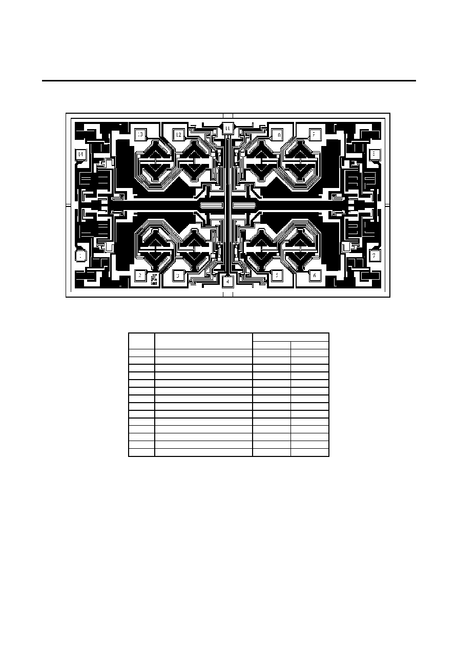
Schematic Diagram
V
CC
+
Non-inverting
input
Inverting
input
V
CC
_
100
100
200
Output
1 4 MIK084C
Absolute Maximum Ratings
Symbol Parameter
Value
Unit
V
CC
Supply Voltage ≠ (Note 1)
±18
V
V
i
Input Voltage ≠ (Note 3)
±15
V
V
id
Differential Input Voltage ≠ (Note 2)
±30
V
Output Short-circuit Duration (Note 4)
Infinite
T
oper
Operating Free-Air Temperature Range MIK074C
0 to 70
0
C
Note 1: All voltage values, except differential voltage, are with respect to the zero reference level (ground) of the supply voltages where
the zero reference level is the midpoint between V
CC
+
and V
CC
-
.
Note 2: Differential voltages are at the non-inverting input terminal with respect to the inverting input terminal.
Note 3: The magnitude of the input voltage must never exceed the magnitude of the supply voltage or 15 volts, whichever is less.
Note 4: The output may be shorted to ground or to either supply. Temperature and/or supply voltages must be limited to ensure that the
dissipation rating is not exceeded.
Page 1 of 3
Replacement of
TL084C
MIK084C
Quad J-FET Operational
Amplifier
January 2002 - revised June 2002
Electrical Characteristics
V
CC
=
± 15V, T
AMB
= 25
∞C (unless otherwise specified)
Symbol Parameters Min
Typ
Max
Units
V
IO
Input Offset Voltage (R
S
= 50
, V
0
=0)
T
amb
=25
∞C
T
min.
T
amb.
T
max.
3
10
13
mV
DV
IO
Input Offset Voltage Drift
18
µV/∞C
I
IO
Input Offset Current*
T
amb
=25
∞C
T
min.
T
amb.
T
max.
5
100
10
pA
nA
I
IB
Input Bias Current*
T
amb
=25
∞C
T
min.
T
amb.
T
max.
65
400
20
pA
nA
A
VD
Large Signal Voltage Gain (R
L
= 2k
, V
O
=
± 10V)
T
amb
=25
∞C
T
min.
T
amb.
T
max.
25
15
200
V/mV
SVR
Supply Voltage Rejection Ratio (R
S
= 50
, V
0
=0)
T
amb
=25
∞C
T
min.
T
amb.
T
max.
70
70
86
dB
I
CC
Supply Current (Per Amplifier)
T
amb
=25
∞C
T
min.
T
amb.
T
max
1.4
2.5
2.5
mA
V
ICM
Input Common Mode Voltage Range
±11
+15
-12
V
CMR
Common Mode Rejection Ratio (R
S
= 50
, V
0
=0)
T
amb
=25
∞C
70 86
dB
±V
OPP
Output Voltage Swing
R
L
=2 k
T
amb
=25
∞C
R
L
=10k
T
min.
T
amb.
T
max.
R
L
=2k
R
L
=10k
10
12
10
12
12
13.5
V
SR
Slew Rate (V
i
= 10V, R
L
= 2k
, C
L
= 100pF,
T
amb
=25
∞C, unity gain)
8 13 V/
µs
t
r
Rise Time (V
i
= 20mV, R
L
= 2k
, C
L
=100pF,
T
amb
=25
∞C, unity gain)
0.1
µs
K
OV
Overshoot (V
i
= 20mV, R
L
= 2k
, C
L
=100pF, T
amb
=25
∞C, unity gain)
20
%
GBP
Gain Bandwidth Product
3
MHz
R
I
Input Resistance
10
12
THD
Total Harmonic Distortion (f=1kHz, R
L
= 2k
, T
amb
=25
∞C)
0.01
%
e
n
Equivalent input Noise Voltage
(R
S
= 100
, f = 1KHz)
18
nV
Hz
V
O1
/V
O2
Channel Separation (A
V
=100)
120
dB
* The Input bias currents are junction leakage currents which approximately double for every 10
0
C increase in the junction
temperature.
Page 2 of 3