1
MIK
R
O
N
JS
C
∑
h
t
t
p
:
/
/
www.
m
i
k
r
o
n
.
r
u
∑
12
A
u
g
u
s
t
20
03
MIK2575 series ∑ 1A STEP-DOWN SWITCHING REGULATOR
DATA
SHEET
6 F
EBRUARY
2004
N
O
. 00028
R
EV
. 1-04
CONTENTS
Page
GENERAL DESCRIPTION
1
FEATURES
1
APPLICATIONS
1
PIN CONNECTION
AND
DESCRIPTION
2
BLOCK DIAGRAM
AND
TYPICAL
2
ABSOLUTE MAXIMUM RATINGS
2
MIK 2575-12
3
MIK 2575-15
3
MIK 2575-
ADJUSTABLE
3
A
LL
OUTPUT
VOLTAGE
VERSIONS
4
TYPICAL CHARACTERISTICS
5
N
ORMALIZED
O
UTPUT
V
OLTAGE
5
OPERATING RATINGS
2
ELECTRICAL CHARACTERISTICS
3
MIK 2575-3.3
3
MIK 2575-5.0
3
Line Regulation
5
Dropout Voltage
5
CONTENTS
Page
C
URRENT
L
IMIT
5
Q
UIESCENT
C
URRENT
5
S
WITCH
S
ATURATION
V
OLTAGE
5
S
TANDBY
Q
UIESCENT
C
URRENT
5
M
INIMUM
O
PERATING
V
OLTAGE
5
O
SCILLATOR
F
REQUENCY
6
E
FFICIENCY
6
F
EEDBACK
P
IN
C
URRENT
6
S
WITCHING
W
AVEFORMS
6
L
OAD
T
RANSIENT
R
ESPONSE
6
TYPICAL TEST CIRCUIT
7
F
IXED
O
UTPUT
V
OLTAGE
V
ERSION
7
A
DJUSTABLE
O
UTPUT
V
OLTAGE
V
ERSION
7
PHYSICAL DIMENSIONS
AND
MARKING
8
SOT-220-5
8
TO-263-5
8
ORDERING INFORMATION
9
DESCRIPTION
The MIK2575 series of regulators are monolithic
integrated circuits that provide all the active
functions for a step-down (buck) switching
regulator, capable of driving 1A load with
excellent line and load regulation. Requiring a
minimum number of external components, these
regulators are simple to use and include internal
frequency compensation and a fixed-frequency
oscillator.
The MIK2575 series offers a high-efficiency
replacement for popular three-terminal linear
regulators. It substantially reduces the size of
the heat sink, and in some cases no heat sink is
required.
Other features include a guaranteed ±4%
tolerance on output voltage within specified
input voltages and output load conditions, and
±10% on the oscillator frequency. The output
switch includes cycle-by-cycle current limiting,
as well as thermal shutdown for full protection
under fault conditions.
FEATURES
∑
3.3V, 5V, 12V, 15V, and adjustable output
versions
∑
Adjustable version output voltage range,
1.23V to 37V ±4% max over line and load
conditions
∑
Guaranteed 1A output current
∑
Wide input voltage range
∑
Requires only 4 external components
∑
52 kHz fixed frequency internal oscillator
∑
TTL shutdown capability, low power standby
mode
∑
Uses readily available standard inductors
∑
Thermal shutdown and current limit
protection
APPLICATIONS
∑
Simple high-efficiency step-down (buck)
regulator
∑
Efficient pre-regulator for linear regulators
∑
On-card switching regulators
∑
Positive to negative converter (Buck-Boost)
REPLACEMENT OF:
LM2575
MIK2575 series
1A STEP-DOWN SWITCHING REGULATOR
2
Design by Vladimir F.Lityaghin / E-mail: lityaghin@mail.ru / Tel: +7(095)532-64-54
MIKR
O
N
J
S
C
∑
h
t
t
p
:
/
/
w
w
w
.
m
i
k
r
o
n
.
r
u
∑
1
2
A
u
gu
s
t
20
03
1A STEP-DOWN SWITCHING REGULATOR ∑ MIK2575 series
PIN
SYMBOL
DESCRIPTION (REFER TO FIGURE 1)
1
V
IN
This pin is the positive input supply for the
MIK2575 step≠down switching regulator. In order
to minimize voltage transients and to supply the
switching currents needed by the regulator, a
suitable input bypass capacitor must be present
(C
IN
in Figure 1).
2
V
OUT
This is the emitter of the internal switch. The
saturation voltage V
SAT
of this output switch is
typically 1.5V. It should be kept in mind that the
PCB area connected to this pin should be kept to
a minimum in order to minimize coupling to
sensitive circuitry.
3
GND
Circuit ground pin. To maintain output voltage
stability, the power ground connections must be
low-impedance (see page 7, Figure 2). Both the
TAB and pin 3 are ground and either connection
may be used, as they are both part of the same
copper lead frame.
4
Feedback
5
_____
ON/OFF
For normal operation, this pin should be grounded or driven with a low-level TTL voltage (typically below
1.6V). To put the regulator into standby mode, drive this pin with a high-level TTL or CMOS signal. This pin can
be safely pulled up to +V
IN
without a resistor in series with it. This pin should not be left open.
This pin senses regulated output voltage to complete the feedback loop. The signal is divided by the internal
resistor divider network R2, R1 and applied to the non≠inverting input of the internal error amplifier. In the
Adjustable version of the MIK2575 switching regulator this pin is the direct input of the error amplifier and the
resistor network R2, R1 is connected externally to allow programming of the output voltage.
O
UTPUT
V
OLTAGE
V
ERSION
R2 (k)
3.3
1.70
5.0
3.10
12.0
8.84
15.0
11.30
F
OR
ADJUSTABLE
VERSION
R1= open, R2= 0
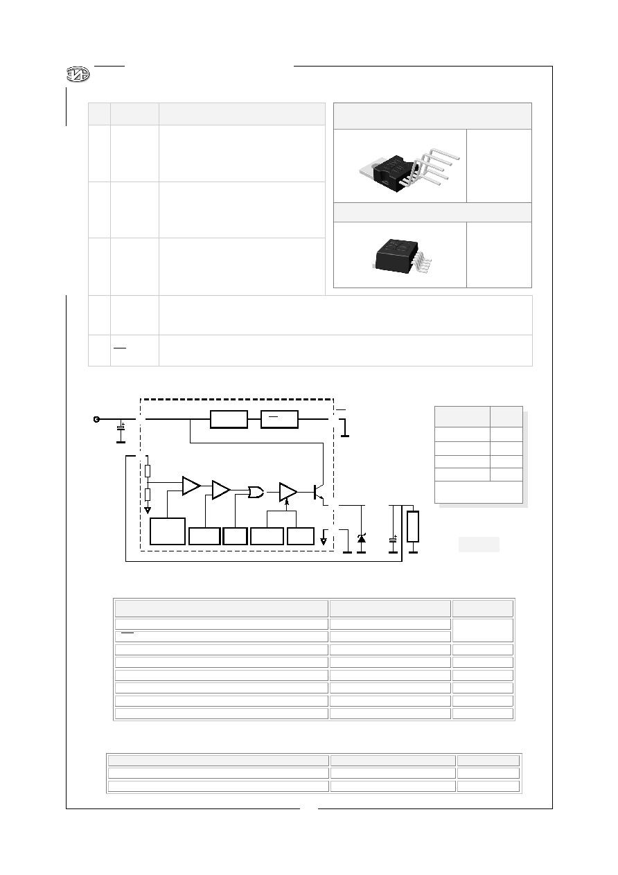
BLOCK DIAGRAM
AND
TYPICAL APPLICATION
ABSOLUTE MAXIMUM RATINGS
OPERATING RATINGS
PIN CONNECTION
AND
DESCRIPTION
MIK2575
T
, MIK2575-xx
T
TO-220-5
TAB
-- ADJ/GND
1 -- V
IN
2 -- V
OUT
3 -- ADJ/GND
4 -- F
EEDBACK
5 -- ON/OFF
MIK2575
S
, MIK2575-xx
S
TO-263-5
TAB
-- ADJ/GND
1 -- V
IN
2 -- V
OUT
3 -- ADJ/GND
4 -- F
EEDBACK
5 -- ON/OFF
Figure 1
PARAMETER
MAXIMUM
UNIT
Maximum Supply Voltage
45
ON/OFF Pin Input Voltage
-0.3V
V
+V
IN
V
Output Voltage to Ground (Steady State)
-1
V
Power Dissipation
Internally Limited
W
Storage Temperature Range
-65 to +150
∞
C
Maximum Junction Temperature
150
∞
C
Minimum ESD Rating (C= 100pF, R = 1.5 k
)
2 kV
Lead Temperature (Soldering, 10 Seconds)
260
∞
C
PARAMETER
VALUE
UNIT
Temperature Range
-40
T
J
+125
∞
C
Supply Voltage
40 V
2
4
TAB
5
1
3
5
1
TAB
Internal
Regulator
ON/OFF
L
O
A
D
!
!!!!
Unregulated
DC Input
+V
IN
+
-
-
+
V
OUT
FEEDBACK
OUTPUT
Regulated
Output
GND
Comparator
Driver
3A
Switch
52 kHz
Oscillator
1.23V
Band-Gap
Reference
Reset
Fixed Gain
Error Amplifier
ON/OFF
!
!
!
1
3
5
C
IN
C
OUT
D1
L1
R2
R1
1k
!
4
!
2
∑
∑
∑
∑
∑
∑ ∑
Thermal
Shutdown
Current
Limit

3
MIK
R
O
N
JS
C
∑
h
t
t
p
:
/
/
www.
m
i
k
r
o
n
.
r
u
∑
12
A
u
g
u
s
t
20
03
MIK2575 series ∑ 1A STEP-DOWN SWITCHING REGULATOR
MIK2575-3.3
MIK2575-5.0
MIK2575-12
MIK2575-15
A
DJUSTABLE
- MIK2575
__
ELECTRICAL CHARACTERISTICS
(NOTE 1)
TEST CIRCUIT OF FIGURE 2, PAGE 7
SYMBOL
PARAMETER
CONDITIONS
MIN
TYP
MAX
UNIT
V
IN
=12V, I
LOAD
=0.2A, T
J
= 25∞C
4.90
5.10
V
OUT
Output
Voltage
8.0V V
IN
40V, 0.2A I
LOAD
1.0A;
T
J
= 25∞C
T
J
= -40∞C to 125∞C
4.80
4.75
5.0
5.20
5.25
V
Efficiency
V
IN
=12V, I
LOAD
=1A
-- 77 -- %
SYMBOL
PARAMETER
CONDITIONS
MIN
TYP
MAX
UNIT
V
IN
=25V, I
LOAD
=0.2A, T
J
= 25∞C
11.76
12.24
V
OUT
Output
Voltage
15V V
IN
40V, 0.2A I
LOAD
1.0A;
T
J
= 25∞C
T
J
= -40∞C to 125∞C
11.52
11.40
12
12.48
12.60
V
Efficiency
V
IN
=15V, I
LOAD
=1A
--
88
--
%
SYMBOL
PARAMETER
CONDITIONS
MIN
TYP
MAX
UNIT
V
IN
= 30V, I
LOAD
=0.2A, T
J
= 25∞C
14.70
15.30
V
OUT
Output
Voltage
18V V
IN
40V, 0.2A I
LOAD
1.0A;
T
J
= 25∞C
T
J
= -40∞C to 125∞C
14.40
14.25
15
15.60
15.75
V
Efficiency
V
IN
=18V, I
LOAD
=1A
-- 88 -- %
SYMBOL
PARAMETER
CONDITIONS
MIN
TYP
MAX
UNIT
V
IN
=12V, I
LOAD
=0.2A, V
OUT
= 5.0V
T
J
= 25∞C
1.217
1.243
V
OUT
Output
Voltage
8V V
IN
40V, 0.2A I
LOAD
1.0A, V
OUT
= 5V
T
J
= 25∞C
T
J
= -40∞C to 125∞C
1.193
1.180
1.23
1.267
1.280
V
Efficiency
V
IN
=12V, I
LOAD
=1A, V
OUT
= 5V
--
77
--
%
Note 1: External components such as the catch diode, inductor, input and output capacitors can affect
switching regulator system performance. When the MIK5275 is used as shown in the figure 2 test
circuit, system performance will be as shown in system parameters section of Electrical
Characteristics.
SYMBOL
PARAMETER
CONDITIONS
MIN
TYP
MAX
UNIT
V
IN
=12V, I
LOAD
=0.2A, T
J
= 25∞C
3.234
3.366
V
OUT
Output
Voltage
4.75V V
IN
40V, 0.2A I
LOAD
1.0A;
T
J
= 25∞C
T
J
= -40∞C to 125∞C
3.168
3.135
3.3
3.432
3.465
V
Efficiency
V
IN
=12V, I
LOAD
=1A
--
75
--
%
4
Design by Vladimir F.Lityaghin / E-mail: lityaghin@mail.ru / Tel: +7(095)532-64-54
MIKR
O
N
J
S
C
∑
h
t
t
p
:
/
/
w
w
w
.
m
i
k
r
o
n
.
r
u
∑
1
2
A
u
gu
s
t
20
03
1A STEP-DOWN SWITCHING REGULATOR ∑ MIK2575 series
Note 2: Output (pin 2) sourcing current. No diode, inductor or capacitor connected to output pin.
Note 3: Feedback (pin 4) removed from output and connected to 0V.
Note 4: Feedback (pin 4) removed from output and connected to +12V for Adjustable, 3.3V and 5V versions,
and +25V for the 12V and 15 V versions, to force the output transistor OFF.
Note 5: V
IN
= 40V.
Note 6: The oscillator frequency reduces to approximately 18 kHz in the event of an output short or an
overload which causes the regulated output voltage to drop approximately 40% from the nominal
output voltage. This self protections feature lowers the average power dissipation of the IC by
lowering the minimum dury cycle from 5% down to approximately 2%.
ELECTRICAL CHARACTERISTICS
(CONTINUED)
T
EST
CIRCUIT
OF
F
IGURE
2,
PAGE
7
V
IN
= 12V for the 3.3V, 5.0V, and Adjustable version
V
IN
= 25V for the 12V version
V
IN
= 30V for the 15V version
I
LOAD
= 200 mA
For typical values T
J
= 25∞C, for min/max values T
J
is the operating junction temperature range that applies,
unless otherwise noted.
A
LL
O
UTPUT
V
OLTAGE
V
ERSIONS
SYMBOL PARAMETER
CONDITIONS
MIN
TYP
MAX
UNIT
DEVICE PARAMETERS
I
B
Feedback Bias
Current
V
OUT
=5V (Adjustable Version Only)
T
J
= 25∫C
T
J
= -40∫C to +125∫C
--
--
50
--
100
500
nA
F
OSC
Oscillator Frequency
(Note 6)
T
J
= 25∫C
T
J
= -40∫C to +125∫C
47
42
52
--
58
63
kHz
V
SAT
Saturation Voltage
I
OUT
=1A (Note 4)
T
J
= 25∫C
T
J
= -40∫C to +125∫C
--
--
0.9
--
1.2
1.4
V
DC
Max Duty Cycle (ON) (Note 3)
93 98 -- %
I
CL
Current Limit
(Notes 2, 6)
T
J
= 25∫C
T
J
= -40∫C to +125∫C
1.7
1.3
2.2
--
3.0
3.2
A
I
L
Output Leakage
Current
T
J
= 25∫C (Notes 4, 5)
Output = 0V
Output = -1V
--
--
7.5
2
30
mA
I
Q
Quiescent Current
(Note 4)
T
J
= 25∫C
--
5.0
10.0
mA
I
STBY
Standby Quiescent
Current
___
ON/OFF Pin = 5V (OFF)
T
J
= 25∫C
-- 50
200
µA
___
ON/OFF CONTROL
V
IH
V
OUT
= 0V
T
J
= 25∫C
T
J
= -40∫C to +125∫C
2.2
2.4
1.4
--
--
--
V
V
IL
__
ON/OFF Pin
Logic Input Level
V
OUT
= Nominal Output Voltage
T
J
= 25∫C
T
J
= -40∫C to +125∫C
--
--
1.2
--
1.0
0.8
V
I
IH
__
ON/OFF Pin = 5V (OFF), T
J
= 25∫C
-- 12 30
I
IL
__
ON/OFF Pin Input
Current
__
ON/OFF Pin = 0V (ON), T
J
= 25∫C
-- 0 10
µA

5
MIK
R
O
N
JS
C
∑
h
t
t
p
:
/
/
www.
m
i
k
r
o
n
.
r
u
∑
12
A
u
g
u
s
t
20
03
MIK2575 series
∑ 1A STEP-DOWN SWITCHING REGULATOR
TYPICAL CHARACTERISTICS
N
ORMALIZED
O
UTPUT
V
OLTAGE
L
INE
R
EGULATION
D
ROPOUT
V
OLTAGE
C
URRENT
L
IMIT
Q
UIESCENT
C
URRENT
S
WITCH
S
ATURATION
V
OLTAGE
S
TANDBY
Q
UIESCENT
C
URRENT
M
INIMUM
O
PERATING
V
OLTAGE
T
J
- JUNCTION TEMPERATURE (∫C)
V
OU
T
-
O
U
T
P
UT
V
O
L
T
AGE
C
H
AN
G
E
(%
)
0
0
25
-25
-50
0.2
-0.2
-0.4
-0.6
-0.8
0.4
0.6
0.8
1.0
-1.0
50
75
100
125
V
I
T
IN
LOAD
J
= 20 V
= 200 mA
Normalized at = 25∞C
= 200mA
I
LOAD
= 1A
I
LOAD
T
J
- JUNCTION TEMPERATURE (∫C)
I
N
P
U
T
--
O
U
T
P
U
T
D
I
F
F
E
R
E
N
T
IA
L
(
V
)
0
0
25
-25
-50
0.5
1.5
1.0
2.0
50
75
100
125
= 5%
= 0.2
V
R
OUT
IND
T
J
- JUNCTION TEMPERATURE (∫C)
I
OU
T
-
O
U
TP
U
T
CU
R
R
E
N
T
(A
)
0
25
-25
-50
0
1
2
3
50
75
100
125
V
IN
= 25 V
SWITCH CURRENT (A)
V
--
SA
T
U
R
A
T
I
O
N
V
O
L
T
AG
E
SA
T
(
V
)
0.2
0.4
0.6
0.8
1.0
0.6
0.4
1.2
0.8
1.0
-40∞C
25∞C
125∞C
V
IN
= 40V
V
IN
= 12V
V
ON/OFF
= 5V
T
J
- JUNCTION TEMPERATURE (∫C)
I S
T
A
N
D
B
Y
Q
U
I
E
S
C
E
N
T
C
U
R
R
E
N
T
ST
BY
--
(
µ
A)
0
0
25
-25
-50
20
40
60
80
100
120
140
160
180
200
50
75
100
125
V
IN
- INPUT VOLTAGE (V)
I
Q
U
I
E
S
C
E
N
T
C
U
R
R
E
N
T
Q
--
(
m
A)
0
25
15
5
35
30
20
10
40
4
6
8
10
12
14
16
18
20
= 5V measured at Ground Pin
= 25∞C
V
T
OUT
J
= 200mA
I
LOAD
= 1A
I
LOAD
V
IN
- INPUT VOLTAGE (V)
V
OU
T
-
O
U
T
P
UT
V
O
L
T
AG
E
C
H
AN
GE
(%
)
0
0
25
15
5
35
30
20
10
40
1.0
0.8
0.6
0.4
0.2
-0.2
-0.4
-0.6
1.2
1.4
= 200 mA
= 25∞C
I
T
LOAD
J
3.3V, 5V and ADJ
12V and 15V
Adjustable Version Only
V 1.23 V
I
= 200 mA
OUT
LOAD
T
J
- JUNCTION TEMPERATURE (∫C)
V
IN
-
I
N
P
U
T
V
O
L
T
A
G
E
(V
)
0
0
25
-25
-50
0.5
1.0
1.5
2.5
3.5
4.5
2.0
3.0
4.0
5.0
50
75
100
125