Replacement of
ULN2801/02/03/04/05/23/24
MIK2801/02/03/04/05/23/24
High-Voltage, High-
Current Darlington
Array (Eight Pairs)
September 1996 ≠ revised April 2001
Desription
The series MIK2801 - MIK2824 are high voltage, high current darlington arrays each containing eight open collector darlington pairs with
common emitters. Each channel is rated at 500mA and can withstand peak currents of 600mA.
Suppression diodes are included for inductive load driving and the inputs are pinned opposite the outputs to simplify board layout.
Features
∑ Eight darlington pairs per package
∑ Output current 500 mA per driver (600 mA peak)
∑ Output voltage 50V (MIK280X)
95V (MIK 282X)
∑ Integral suppression diodes for inductive loads
∑ Outputs can be paralleled for higher current
∑ TTL/CMOS/PMOS/DTL compatible inputs
∑ Inputs pinned opposite outputs to simplify layout
The five versions interface to all common logic families
MIK2801
General purpose, DTL, TTL, PMOS, CMOS
MIK2802
14-25 V PMOS
MIK2803, MIK2823
5 V TTL, CMOS
MIK2804, MIK2824
6-15 V CMOS, PMOS
MIK2805
2-5 V CMOS, PMOS
These devices are useful for driving a wide range of loads including solenoids, relays DC motors, LED displays, filament lamps and high
power buffers. The MIK2801-MIK2824 are supplied in 18 pin plastic DIP packages with a copper leadframe to reduce thermal
resistance.
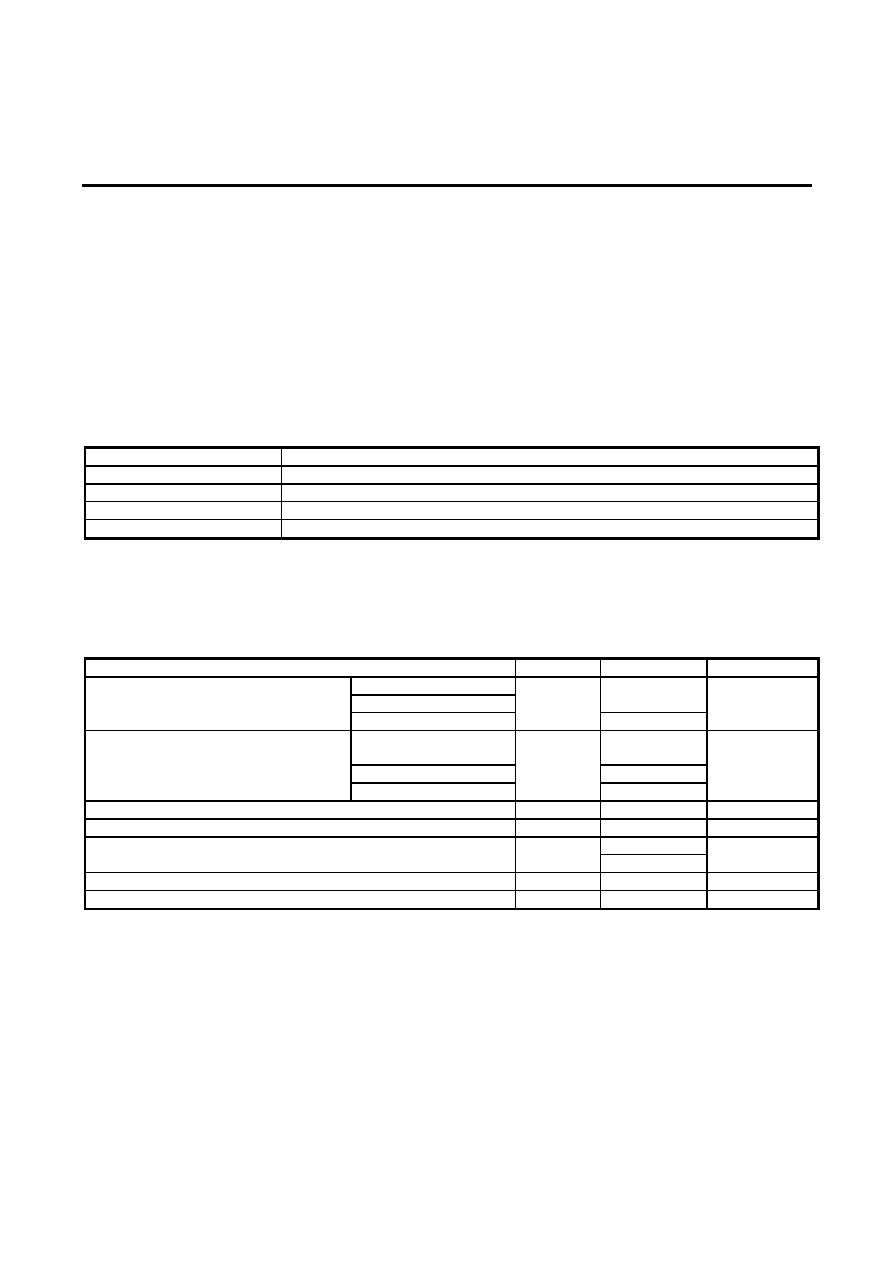
Absolute Maximum Ratings
Characteristic Symbol
Limits
Unit
Typ
MIK2801-MIK2805
50
Output voltage
MIK2823-MIK2824
V
CE
95
V
Typ
MIK2801-2804, 2823, 2824
30
Input voltage
MIK2805
V
IN
15
V
Continuous collector current
I
C
500 mA
Continuous base current
I
IN
25 mA
1
Power dissipation at T
amb
= 25
o
C (one Darlington pair)
total package
P
tot
2
W
Operating ambient temperature range
T
amb
-20 to +85
o
C
Storage temperature range
T
stg
-55
to+150
o
C
Page 1 of 3

Replacement of
ULN2801/02/03/04/05/23/24
MIK2801/02/03/04/05/23/24
High-Voltage, High-
Current Darlington
Array (Eight Pairs)
September 1996 ≠ revised April 2001
Electrical characteristics
T
A
= +25
0
C (unless otherwise noted)
Characteristics Symbol Device Test
Condition
Min
Typ
Max
Units
MIK2801 to MIK2805
V
CE
=50V T
A
=25
o
C
V
CE
=50V T
A
=70
o
C
< 1
< 1
50
100
Output Leakage Current
I
CEX
MIK2823, MIK2824
V
CE
=95V T
A
=25
o
C
V
CE
=95V T
A
=70
o
C
< 1
< 1
50
100
µA
I
C
=100mA
I
B
=250
µA
0.9
1.1
I
C
=200mA
I
B
=350
µA
1.1
1.3 V
Collector-Emitter Saturation
Voltage
V
CE(SAT)
All
I
C
=350mA
I
B
=500
µA
1.3
1.6
MIK2802 V
IN
=17V
0.82
1.25
MIK2803, MIK2823
V
IN
=3.85V
0.93
1.35
MIK2804, MIK2824
V
IN
=5.0V
0.35
0.5
I
IN(ON)
MIK2805 V
IN
=3.0V
1.5
2.4
mA
Input Current
I
IN(OFF)
All
I
C
=500
µA T
A
=70
o
C
50 65
µA
MIK2802 V
CE
=2.0V
I
C
=300mA
13
MIK2803, MIK2823
V
CE
=2.0V
I
C
=300mA
3.0
MIK2804, MIK2824
V
CE
=2.0V
I
C
=350mA
8.0
Input Voltage
V
IN(ON)
MIK2805 V
CE
=2.0V
I
C
=350mA
2.4
V
DC Forward Current Transfer
Ratio
h
FE
MIK2801
V
CE
=2.0V
I
C
=350mA
1000
Turn-On Delay
t
PLH
All
0.5
V
IN
to 0.5 V
OUT
0.25
1.0
µS
Turn-Off Delay
t
PHL
All
0.5
V
IN
to 0.5 V
OUT
0.25
1.0
µS
V
R
=50V T
A
=25
o
C 50
MIK2801 to MIK2805
V
R
=50V T
A
=70
o
C 100
V
R
=95V T
A
=25
o
C 50
Clamp Diode Leakage
Current
I
R
ULN2823, ULN2824
V
R
=95V T
A
=70
o
C 100
µA
Clamp Diode Forward Voltage
V
F
All
I
F
=350mA
1.7
2.0
V
Input Capacitance
C
IN
All
15 25 pF
Connection Diagram
Page 2 of 3

Replacement of
ULN2801/02/03/04/05/23/24
MIK2801/02/03/04/05/23/24
High-Voltage, High-
Current Darlington
Array (Eight Pairs)
September 1996 ≠ revised April 2001
Pad Location MIK28XX
Chip size: 2.8 x 1.5 mm
Pad Location Coordinates (Note1)
Coordinates(µm)
Pad N
Pad name
X Y
1 IN1
105
330
9a
GND (out 1,2), Note 2
365
215
2 IN2
555
100
3 IN3
790
100
9b
GND (out 3,4), Note 2
1030
100
4 IN4
1270
100
5 IN5
1510
100
9c
GND (out 5,6), Note 2
1700
100
6 IN6
1955
100
7 IN7
2205
100
9d
GND (out 7,8), Note 2
2575
105
8 IN8
2575
365
10a
COM, Note 3
2575
675
10b
COM, Note 3
2575
815
11 OUT8
2355
1145
12 OUT7
2065
1145
13 OUT6
1770
1145
14 OUT5
1480
1145
15 OUT4
1185
1145
16 OUT3
895
1145
17 OUT2
605
1145
18 OUT1
105
755
Note 1: Chip carrier must be connected with 9 lead of package by two wire.
Note 2: Pads 9a, 9b, 9c, 9d must be connected to chip carrier.
Note 3: Pads 10a, 10b must be connected with 10 lead of package.
Page 3 of 3