 | –≠–ª–µ–∫—Ç—Ä–æ–Ω–Ω—ã–π –∫–æ–º–ø–æ–Ω–µ–Ω—Ç: MIK3800 | –°–∫–∞—á–∞—Ç—å:  PDF PDF  ZIP ZIP |
Replacement of
MB3800
MIK3800
Bipolar Switching
Regulator Controller
July 2001 ≠ revised July 2002
Description
The MIK3800 is a single-channel switching regulator control IC for low voltage applications incorporating a soft start function and short
circuit detection function. The device has a low minimum operating voltage of 1.8 V and is ideal for the supply of battery-operated
electronic equipment
Features
∑ Wide supply voltage operating range:1.8 to 15 V
∑ Low current consumption: Typically 5.5 mA in operation,
1µA or less in stand-by
∑ High speed operation is possible: Maximum 1MHz
∑ The error amplifier gain is set inside the IC, so peripheral
components are minimized.
∑ Incorporates a soft start circuit.
∑ Incorporates a timer-latch type short circuit detection circuit
(SCP).
∑ Totem-pole type output wich adjustable on/off current (for
NPN transistors).
∑ Incorporates a stand-by function.
∑ Three types of packages (SOP-8 or SOL-8, SSOP-8).
Pin assignment
1
SCP
Vcc
BR/CTL
OSC
GND
OUT
2
3
4
8
7
6
5
(FPT-8P-M03)
(FPT-8P-M02)
(FPT-8P-M01)
Pin Description
Pin
Symbol
I/O
Description
1
-IN
I
Error amplifier inverting input pin
2
SCP
--
Soft start and SCP setting capacitor connection pin
3
VCC
--
Power supply pin
4
BR/CTL
I
Output current setting and control pin
5
OUT
O
Totem-pole type output pin
6 GND --
Ground
pin
7
OSC
--
Capacitor and resistor connection pin for setting the oscillation frequency
8
FB
O
Error amplifier output pin
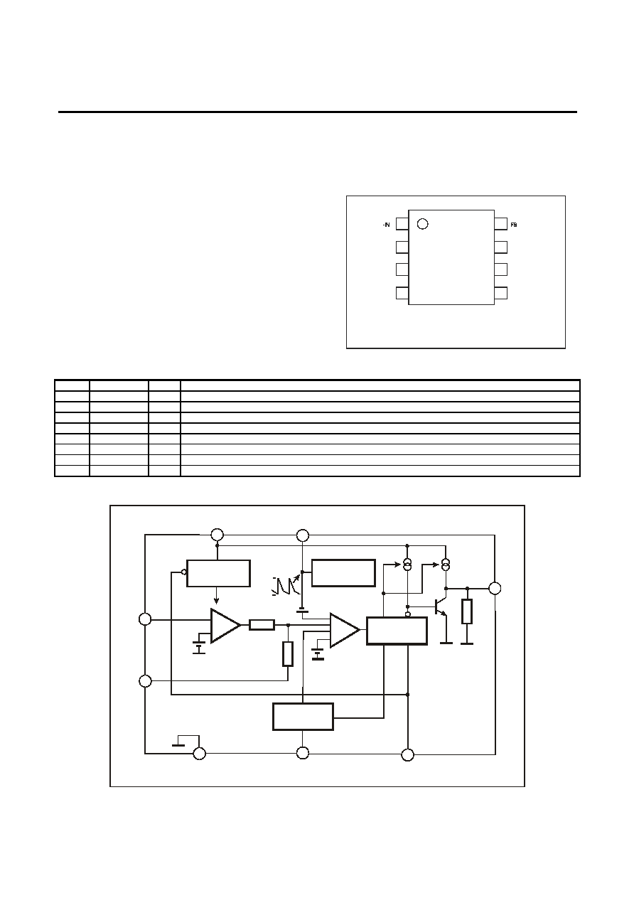
Block Diagram
Soft start SCP
+
-
6
2
4
5
7
3
Reference
Voltage Supply
Sawtooth wave
oscillator
Output drive
control circuit
+
-
+
+
1.25 V
0.5 V
36 k
500
0.3 V
GND
SCP
BR/CTL
8
1
FB
-IN
DTC 0.6 V
Error Amp.
PWM
Comp.
30 k
OUT
OSC
Vcc
0.6 V
0.1 V
Page 1 of 9

Replacement of
MB3800
MIK3800
Bipolar Switching
Regulator Controller
July 2001 ≠ revised July 2002
Absolute maximum ratings
(Ta = +25∞ C)
Rated Value
Parameter Symbol Condition
Min Max
Units
Power supply voltage
VCC
--
16
V
Output source current
IO+
--
-50
mA
Output sink current
IO-
--
-- 50 mA
SOP-8, Ta
+25∞C
--
570* mW
SOP-8, Ta
+25∞C
--
430* mW
Allowable dissipation
PD
SSOP-8, Ta
+25∞C
--
580* mW
Operating temperature
Top
-30
+85
∞C
Storage temperature
Tstg
--
-55 +125 ∞C
* - When mounted on a 10 cm square double-sided epoxy board.
WARNING : Semiconductor devices can be permanently damaged by application of stress (voltage, current, temperature, etc.) in
excess of absolute maximum ratings. Do not exceed these ratings.
Recommended operating conditions
(T
a
= +25∞ C)
Values
Symbol Parameter
Min Typ Max
Units
VCC
Power supply voltage
1.8
--
15
V
VI
Error amplifer input voltage
-0.2
--
1.0
V
VBR
BR/CTL pin input voltage
-0.2
--
Vcc
V
IO+
Output source current
-40
--
--
mA
IO-
Output sink current
--
--
40
mA
CPE
SCP pin capacitance
--
0.1
--
µF
CP
Phase compensation capacitance
--
0.1
--
µF
RB
Output current setting resistance
150
390
5000
RT Timing
resistance
1.0 3.0 10.0 k
CT Timing
capacitance
100
270 10000 pF
fOSC Oscillation
frequency
10 500 1000 kHz
TOP Operating
temperature
-30 +25 +85
∞C
WARNING : Recommended operating conditions are normal operating ranges for the semiconductor device. All the device's electrical
characteristics are warranted when operated within these ranges. Always use semiconductor devices within the
recommended operating conditions. Operation outside these ranges may adversely affect reliability and could result in
device failure. No warranty is made with respect to uses, operating conditions, or combinations not represented on the
data sheet.
Page 2 of 9

Replacement of
MB3800
MIK3800
Bipolar Switching
Regulator Controller
July 2001 ≠ revised July 2002
Electrical characteristics
(V
CC
= +2V, T
a
= 25
o
C )
Value
Parameter Symbol
Condition
Min Typ Max
Units
Reset voltage
V
R
--
--
0.9
V
Circuit to prevent malfunction at low
input voltage (U.V.L.O.)
Threshold voltage
V
TH
--
1.1 1.3 1.5 V
Charging current
I
CS
V
SCP
= 0 V
-1.5
-1.0
-0.7
µA
Soft start
Voltage at soft start completion
V
tS
-- 0.7
0.8
0.9
V
Charging current
I
CPC
V
SCP
= 0 V
-1.5
-1.0
-0.7
µA
Short circuit detection (S.C.P.)
Threshold voltage
V
tPC
-- 0.7
0-.8
0.9
V
Oscilation frecuency
f
OSC
R
T
= 3.0 k
, C
T
=270
pF
400 500 600 kHz
Frecuency input stability
f
dV
V
CC
= 2 V to 15 V
--
2
10
%
Sawtooth wave oscillator (OSC)
Frecuency variation with
temperature
f
dT
T
a
= -30
∞C to +85∞C
-- 5 -- %
Input threshold voltage
V
T
V
FB
= 450 mV
480
500
520
mV
V
T
input stability
V
TdV
V
CC
= 2 V to 15 V
--
5
20
mV
V
T
variation with temperature
V
TdT
T
a
= -30
∞C to +85∞C
-- 1 -- %
Input bias current
I
B
V
IN
= 0 V
-1.0
-0.2
1.0
µA
Voltage gain
A
V
-- 70
100
145
V/V
Frecuency bandwidth
BW
A
V
= 0 dB
--
6
--
MHz
V
OM
+ 0.78
0.87
--
V
Maximum output voltage range
V
OM
-
--
-- 0.05 0.2 V
Output source current
I
OM
+ --
-40
-24
µA
Error amplifier
Output sink current
I
OM
-
V
FB
= 0.45 V
24 40 --
µA
Idle period adjustment section
Maximum duty cycle
t
DUTY
R
T
= 3.0 k
, C
T
=270
pF V
FB
= 0.8 V
65 75 85 %
V
OH1
R
B
= 390
, I
O
= -15
mA
1.0 1.2 -- V
V
OH2
R
B
= 750
, V
CC
= 1.8
V, I
O
=-10 mA
0.8 1.0 -- V
V
OL1
R
B
= 390
, I
O
=15 mA
-- 0.1 0.2 V
Output voltage
V
OL2
R
B
= 750
, V
CC
= 1.8
V, I
O
= 10 mA
-- 0.1 0.2 V
Output source current
I
O
+
R
B
= 390
, V
O
= 0.9 V
-- -30 -20 mA
Output sink current
I
O
-
R
B
= 390
, V
O
= 0.3 V
30 60 -- mA
Output section
Pull down resistance
R
O
-- 20
30
40
k
Pin voltage
V
BR
R
B
= 390
0.2 0.3 0.4 V
Input off condition
I
OFF
-20
--
0
µA
Input on condition
I
ON
--
--
-45
µA
Output current setting
section/Control section
Pin current range
I
BR
--
-1.8 -- -0.1 mA
Stand-by current
I
CCS
BR/CTL pin open or
V
CC
-- -- 1
µA
Entire device
Averge supply current
I
CC
R
B
= 390
-- 5.5 9.3 mA
Page 3 of 9

Replacement of
MB3800
MIK3800
Bipolar Switching
Regulator Controller
July 2001 ≠ revised July 2002
Diagram
Output
short
circuit
Soft start
t
PE
Output short
circuit
Short circuit
detection
t
S
OFF
Power supply control SW
ON
SPC pin waveforms
OUT pin waveforms
Soft start setting voltage
Sawtooth wave output
Idle period setting voltage
Reference input for short circuit
detection comparator
FB pin voltage
How to set the time constant for soft start and short circuit detection
1. Soft Start
At power on, the capacitor C
PE
connected to the SCP pin starts charging. The PWM comparator compares the soft start setting voltage
as a proportion of the voltage at the SCP pin with the sawtooth waveform. The comparison controls the ON duty of the OUT pin, causing
the soft start operation. On completion of soft start operation, the voltage at the SCP pin stays low, the soft start setting voltage stays
high, and the circuit enters the output short circuit detection wait state.
Soft start time (The time until the ON duty reaches approximarely 50%)
t
S
[s]
0.35 x C
PE
[
µF]
2. Short Circuit Protection
If the swithing regulator output suddenly drops due to load effect, the error amplifier output (FB pin) is fixed at VOM+ and capacitor C
PE
starts charging. When the voltage at the SCP pin reaches aproxximately 0.8V, the output pin is set low and the SCP pin stays low.
Once the protection circuit operates, the circuit can be restored by resetting the power supply.
∑
Short circuit detection time
t
PE
[s]
0.8 x C
PE
[
µF]
Page 4 of 9

Replacement of
MB3800
MIK3800
Bipolar Switching
Regulator Controller
July 2001 ≠ revised July 2002
Typical Characteristics
Supply voltage vs. Supply current
Suppl
y
c
u
rren
t
I
CC
(
m
A)
0
2
4
6
8
10
0
4
8
12
16
20
T
a
B
= +25 C
R = 390
0
Supply voltage V
CC
(V)
Supply voltage vs. Input threshold voltage
0
4
8
12
16
0
0.2
0.4
0.6
0.8
0.1
20
T
a
= +25 C
0
Suppl
y
c
u
rren
t
I
CC
(mA)
Supply voltage V
CC
(V)
Inpu
t
t
h
re
sh
o
l
d
vol
t
ag
e
V
(V
)
T
0
0
1.0
2.0
3.0
4.0
5.0
T = +25 C
a
0
Supply voltage V
(V)
CC
Supply voltage vs. Input threshold voltage
0.2
0.4
0.6
0.8
1.0
Ambient temperature vs. Input threshold
voltage variation ratio
-40 -20
0
20
40
60
80
100
-15
-10
-5
0
5
V
= 2 V
CC
Ambient temperature T
a
( C)
0
In
p
u
t
th
r
e
sh
o
l
d
vo
lt
a
g
e
var
i
at
i
o
n
ra
ti
o
V
TT
/V
(%
)
10
0
20
40
60
80
1
0
100
200
300
400
500
Low level output
Lo
w
lev
e
l
ou
t
p
u
t
vo
l
t
a
g
e
V
OU
T
(mV
)
V
= 2 V
R = 390
= 25 C
CC
B
a
0
00
High level output current I
OUT
(mA)
High level output
0
0.4
0.8
1.2
1.6
2.0
0
-10
-20
-30
-40
-50
V
= 2 V
R = 390
= 25 C
CC
B
a
0
High
lev
e
l
o
u
tput
vo
l
t
ag
e
V
OU
T
(V
)
High level output current I
OUT
(mA)
Page 5 of 9