Replacement of
UC3842A/43A/44A/45A
MIK3842A/43A/44A/45A
High Performance Current
Mode PWM Controller
July 1995 ≠revised July 2002
Description
The MIK3842A(AM)/43A(AM)/44A(AM)/45A(AM) are fixed frequency current mode PWM controller. They are specially designed for
OFF
-Line and DC to DC converter applications with a minimal external components. Internally implemented circuits include a trimmed
oscillator for precise duty cycle control, a temperature compensated reference, high gain error amplifier, current sensing comparator,
and a high current totempole output ideally suited for driving a power MOSFET. Protection circuitry includes built undervoltage lockout
and current limiting. The MIK3842A(AM) and MIK3844A(AM) have UVLO thresholds of 16 V (on) and 10 V (off). The corresponding
thresholds for the MIK3843A(AM)/45A(AM) are 8.4V (on) and 7.6V (off). The MIK3842A(AM) and MIK3843A(AM) can operate within 100%
duty cycle. The MIK3844A(AM) and UC3845A(AM) can operate within 50% duty cycle.
The MIK384XA(AM) has Start-Up Current 0.17mA (typ).
Features
∑ Low Start-Up and Operating Current
∑ High Current Totem Pole Output
∑ Undervoltage Lockout With Hysteresis
∑ Operating Frequency Up To 300KHz (MIK384XA)
500KHz (MIK384XAM
)
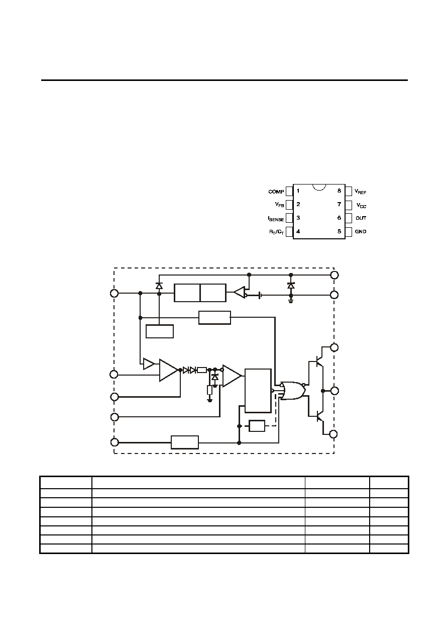
Pin Connection
Top view
Block diagram
(toggle flip flop used only in MIK3844, MIK3845)
7
POWER VCC
OUT
POWER GND
OSCILLATOR
5
36V
GND
7
VCC
2
8
VREF
INTERNAL
BIAS
LOGIC
5V
VREF
SET/
RESET
6
1
+
-
5
4
R /C
T
T
CURRENT
SENSE
COMP
T
R
1/2 VREF
1V
C.S.
COMP
ERR
AMP
VFB
S
PWM
LATCH
3
UVLO
V
GOOD
REF
2R
R
Absolute Maximum Ratings
Symbol Parameter Maximum
Units
V
CC
Supply Voltage (low impedance source)
30
V
I
O
Output
Current
±1
A
V
I
Input Voltage (Analog Inputs pins 2,3)
-0.3 to 5.5
V
I
SINK (E.A)
Error Amp Output Sink Current
10
mA
P
O
Power Dissipation (T
A
=25
0
C) 1
W
Tstg
Storage Temperature Range
-65 to150
o
C
T
L
Lead Temperature (soldering 5 sec.)
260
o
C
Page 1 of 8

Replacement of
UC3842A/43A/44A/45A
MIK3842A/43A/44A/45A
High Performance Current
Mode PWM Controller
July 1995 ≠revised July 2002
Electrical characteristics
(*V
CC
=15V, R
T
=10k
, C
T
=3.3nF, T
A
=0
0
C to +70
0
C, unless otherwise specified)
Characteristics Symbol
Test
Conditions
Min
Typ
Max
Units
Reference Section
Reference Output Voltage
V
REF
T
J
= 25
∞C, I
REF
= 1 mA
4.9 5.0 5.1 V
Line Regulation
V
REF
12V V
CC
25 V
6.0
20
Load Regulation
V
REF
1 mA I
REF
20mA
6.0
25
mV
Short Circuit Output Current
I
SC
T
A
= 25
∞C
-100
-180
mA
Oscillator Section
MIK384XA 47
50
57
Oscillation Frequency
f
T
J
= 25
∞C
MIK384XAM 47
52
57
KHz
Frequency Change with Voltage
f/V
CC
12V V
CC
25 V
0.05
1.0
%
Oscillator Amplitude
V
(OSC)
(peak to peak)
1.6
V
Error Amplifier Section
Input Bias Current
I
BIAS
V
FB
=3V
-0.1
-2
µA
Input Voltage
V
I(E.A)
V
pin1
= 2.5V
2.42
2.5
2.58
V
Open Loop Voltage Gain
A
VOL
2V
V
0
4V
65
90
Power Supply Rejection Ratio
PSRR
12V V
CC
25 V
60
70
dB
Output Sink Current
I
SINK
V
pin2
= 2.7V, V
pin1
= 1.1V
2
7
mA
Output Source Current
I
SOURCE
V
pin2
= 2.3V, V
pin1
= 5V
-0.5
-1.0
mA
High Output Voltage
V
OH
V
pin2
= 2.3V, R
L
= 15K
to GND
5.0 6.0
Low Output Voltage
V
OL
V
pin2
= 2.7V, R
L
= 15K
to PIN 8
0.8
1.1
V
Current Sense Section
Gain G
V
(Note 1 & 2)
2.85
3.0
3.15
V/V
Maximum Input Signal
V
I(MAX)
V
pin1
= 5V (Note1)
0.9
1.0
1.1
V
Supply Voltage Rejection
SVR
12V V
CC
25 V (Note 1)
70
dB
Input Bias Current
I
BIAS
V
pin3
= 3V
-3.0
-10
µA
Output Section
I
SINK
= 20 mA
0.08
0.4
Low Output Voltage
V
OL
I
SINK
= 200 mA
1.4
2.2
I
SINK
= 20 mA
13
13.5
High Output Voltage
V
OH
I
SINK
= 200 mA
12
13.0
V
Rise Time
t
R
T
J
= 25
∞C, C
L
= 1nF (Note 3)
45
150
Fall Time
t
F
T
J
= 25
∞C, C
L
= 1nF (Note 3)
35
150
nS
Undervoltage Lockout Section
MIK3842A(AM)/44A(AM) 14.5
16.0
17.5
Start Theshold
V
TH(ST)
MIK3843A(AM)/45A(AM) 7.8
8.4
9.0
V
MIK3842A(AM)/44A(AM) 8.5
10
11.5
Min. Operating Voltage
(After Turn On)
V
OPR(min)
MIK3843A(AM)/45A(AM) 7.0
7.6
8.2
V
PWM Section
MIK3842A(AM)/43A(AM) 95
97
100
Max. Duty Cycle
D
(MAX)
MIK3844A(AM)/45A(AM) 47
48
50
Min. Duty Cycle
D
(MAX)
0
%
Total Standby Current
Start
-Up Current
I
ST
MIK384XA(AM)
0.17 0.3
Operating Supply Current
I
CC (OPR)
V
pin3
= V
pin2
= 0V
13
17
mA
Zener Voltage
V
Z
I
CC
=25 mA
30
38
V
* - Adjust V
CC
above the start threshold before setting it to 15V.
Note 1: Parameter measured at trip point of latch with V
pin2
=0.
Note 2: Gain defined as A=
V
pin1
/
V
pin3
; 0
V
pin3
0.8V.
Note 3: These parameters, although guaranteed, are not 100% tested in production.
Page 2 of 8

Replacement of
UC3842A/43A/44A/45A
MIK3842A/43A/44A/45A
High Performance Current
Mode PWM Controller
July 1995 ≠revised July 2002
Pin functions
N Function
Description
1
COMP
This pin is the Error Amplifier output and is made for loop compensation.
2 V
FB
This is the inverting input of the Error Amplifier. It is normally connected to the switching power supply
output through a resistor divider.
3 I
SENSE
A voltage proportional to inductor current is connected to this input. The PWM uses this information to
terminate the output switch conduction.
4 R
T
/C
T
The oscillator frequency and maximum Output duty cycle are programmed by connecting resistor R
T
to V
ref
and capacitor C
T
to ground.
5
GROUND
This pin is the combined control circuitry and power ground.
6
OUTPUT
This output directly drives the gate of a power MOSFET. Peak currents up to 1A are sourced and sink by
this pin.
7 V
CC
This pin is the positive supply of the integrated circuit.
8 V
ref
This is the reference output. It provides charging current for capacitor C
T
through resistor R
T
.
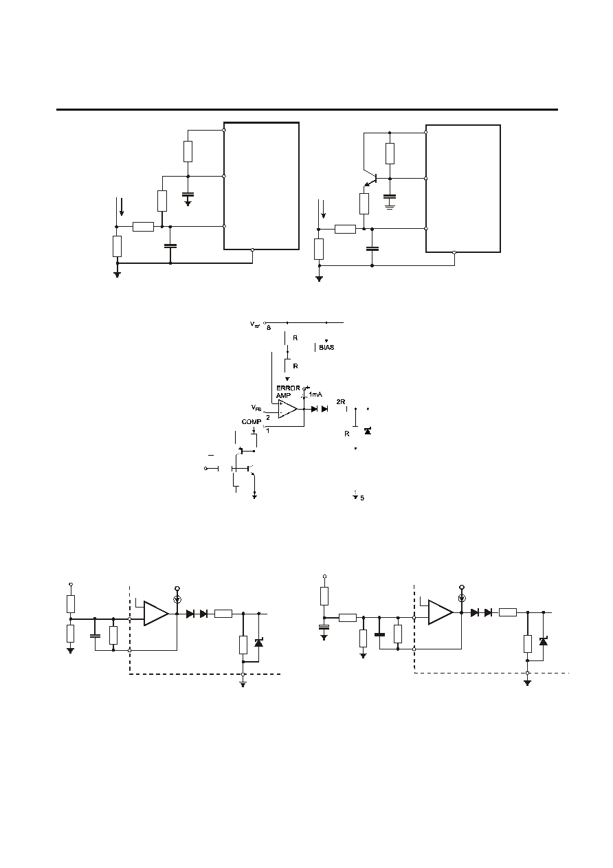
Application information
+
_
2.5V
2
1
1mA
V
FB
COMP
Figure 1. Error Amp Configuration
7
V
ON
MIK3842
MIK3844
MIK3843
MIK3845
V
OFF
16V
10V
8.4V
7.6V
ON/OFF COMMAND TO S/R OF IC
V
CC
I
CC
V
CC
V
OFF
V
ON
13mA
0.2mA
During UVLO, the Output is low
Figure 2. Undervoltage Lockout
ERROR
AMP
2R
2
1
3
5
+
_
R
1V
CURRENT
SENSE
COMPARATOR
R
R
S
C
CURRENT
SENSE
GND
COMP
V
FB
I
S
Peak current is determined by I
S max
1.0V
R
S
Figure 3. Current Sense Circuit
Page 3 of 8
Replacement of
UC3842A/43A/44A/45A
MIK3842A/43A/44A/45A
High Performance Current
Mode PWM Controller
July 1995 ≠revised July 2002
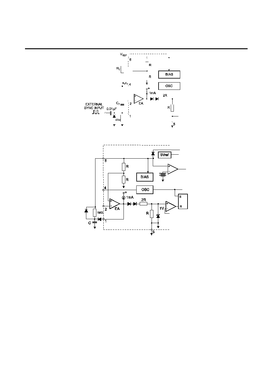
R
1
R
T
R
T
R
SLOPE
R
SLOPE
R
S
R
1
R
S
R
T
/C
T
R
T
/C
T
I
SENSE
I
SENSE
GND
GND
MIK3842
MIK3842
I
S
I
S
V
REF
V
REF
8
4
3
5
8
4
3
5
Figure 4. Slope Compensation Techniques
SCR must be selected for a holding current of less than 0.5mA.
The simple two transistor circuit can be used in place of the SCR as shown.
Figure 5. Latched Shutdown
2R
R
R
I
R
d
C
f
R
f
COMP
EA
From V
0
V
FB
+
-
+
1mA
2.5 V
2
1
5
2R
R
R
p
R
I
R
d
C
f
C
p
R
f
EA
COMP
From V
0
V
FB
+
-
+
2.5 V
2
1
5
1mA
Error Amp compensation circuit for stabilizing any current-mode topology except
for boost and flyback converters operating with continuous inductor current.
Error Amp compensation circuit for stabilizing current-mode boost and flyback
topologies operating with continuous inductor current.
Figure 6. Error Amplifier Compensation
Page 4 of 8
Replacement of
UC3842A/43A/44A/45A
MIK3842A/43A/44A/45A
High Performance Current
Mode PWM Controller
July 1995 ≠revised July 2002
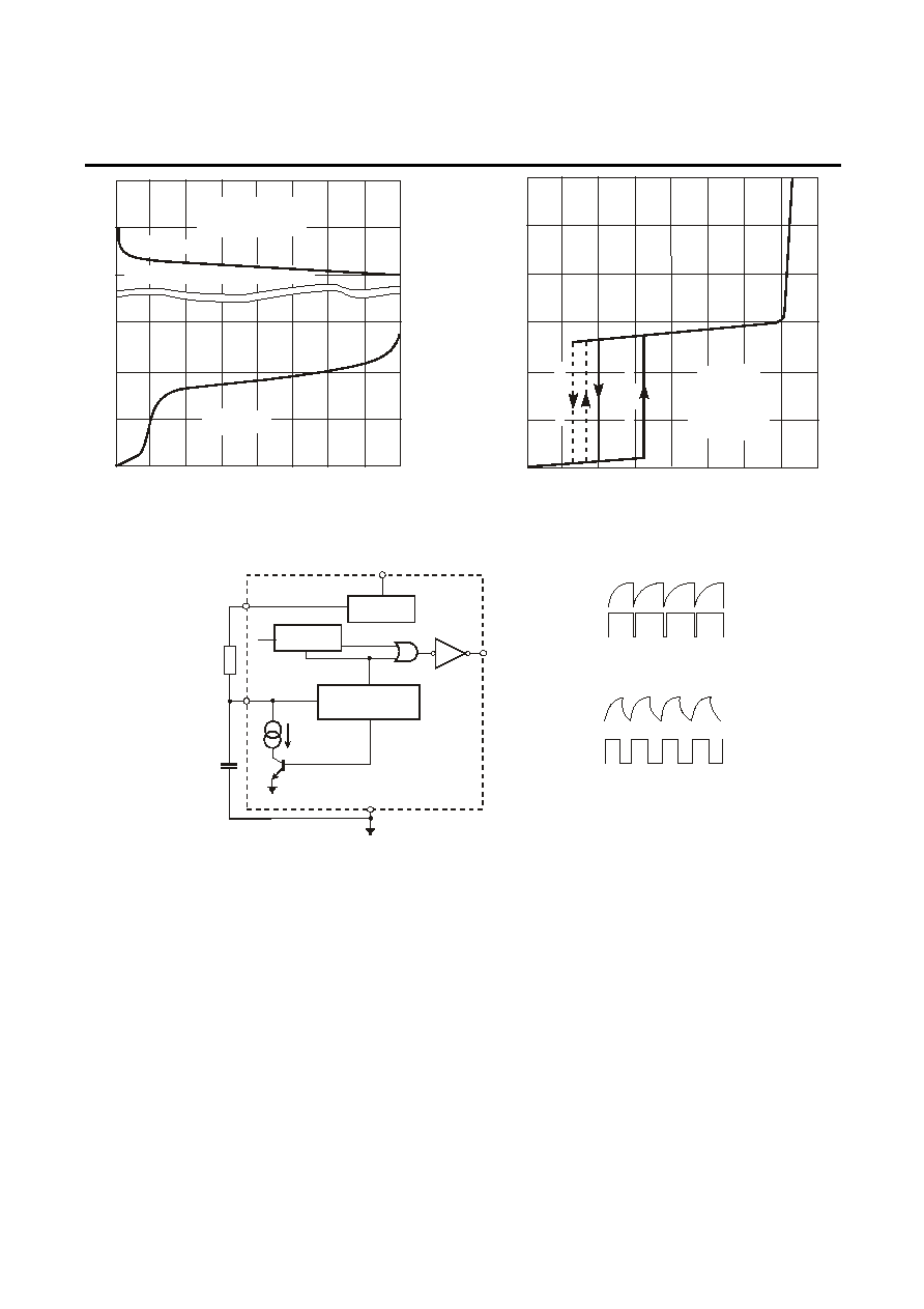
Figure 7. External Clock Synchronization
Figure 8. Soft-Start Circuit
Page 5 of 8
Replacement of
UC3842A/43A/44A/45A
MIK3842A/43A/44A/45A
High Performance Current
Mode PWM Controller
July 1995 ≠revised July 2002
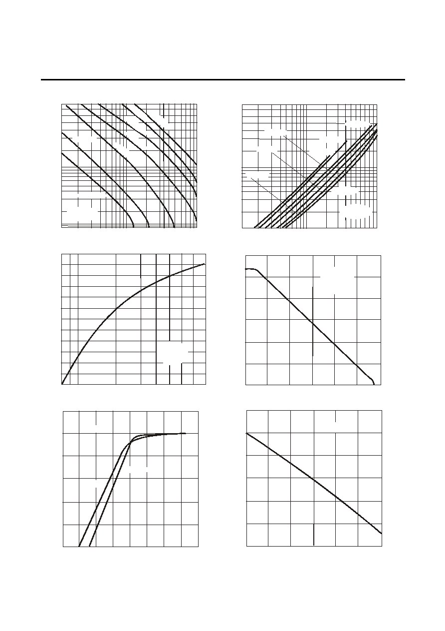
Typical Performance Characteristics
Figure 1.
.
Timing Resistor vs. Oscillator Frequency
10
20
30
50
100
200
300 500
1
2
10
20
50
5
f
(KHz
OSC
R
(K )
T
C = 10nF
T
C = 5nF
T
C
=
2n
F
T
C
=
50
0p
F
T
C
=
20
0p
F
T
C
=
10
0p
F
T
C
=
1n
F
T
V
= 15 V
T = 25 C
CC
A
O
)
Figure 2.
.
Output Dead-Time vs. Oscillator Frequency
10
20
30
50
100
200
300 500
1
2
3
10
20
30
50
5
f
(KHz
OSC
%
V
= 15 V
T = 25 C
CC
A
O
C = 100pF
T
C = 10nF
T
C = 5nF
T
C = 200pF
T
C = 500pF
T
C = 1nF
T
C = 2nF
T
)
Figure 3.
.
Maximum Output Duty Cycle vs.
Timing Resistor (MIK3842/43)
R (K )
T
50
60
70
80
90
40
1
2
3
5
Dm ax
(%)
V
= 15 V
C = 3.3nF
T = 25 C
CC
T
A
O
Figure 4.
.
Error Amp Open-Loop Gain vs.
Frequency
60
80
40
0
20
-20
10
100
1K
10K
100K
1M
f (Hz)
(dB)
V
= 15 V
V = 2V to 4V
R = 100K
T = 25 C
CC
O
L
A
O
Figure 5.
.
Current Sense Input Threshold vs.
Error Amp Output Voltage
V (V)
O
V
(V)
th
0.8
1.0
0.6
0.2
0.4
0
2
4
6
T = 125 C
A
O
T = 25 C
A
O
V
= 15V
CC
Figure 6.
.
Reference Short Circuit Current vs.
Temperature
T ( C)
A
O
90
100
80
60
70
50
0
25
50
75
100
V
= 15 V
CC
I
(mA)
SC
Page 6 of 8
Replacement of
UC3842A/43A/44A/45A
MIK3842A/43A/44A/45A
High Performance Current
Mode PWM Controller
July 1995 ≠revised July 2002
Figure .
.
7 Output Saturation Voltage vs. Load Current
T = 25C
A
I (m A)
O
V
(V)
sat
-2
-1
3
1
2
0
0
200
400
600
Sourse Satura tion
(Load to Ground)
80 s Pulsed Load
120Hz Ra te
µ
V
= 15 V
CC
Sink Saturation
(Load to V
)
CC
Figure .
.
8 Supply Current vs. Supply Voltage
I
(m A)
CC
V
(V)
CC
20
15
5
10
0
0
10
20
30
U
C
3
843/
45
U
C
3842
/
4
4
I
= 0V
V = 0V
R = 10K
T = 25 C
C = 3.3nF
Sense
FB
T
A
T
O
Vref
5V REG
OSCILLATOR
PWM
7
8
CLOCK
4
5
6
GND
OUTPUT
LARGE R / SMALL C
T T
SMALL R / LARGE C
T
T
OUTPUT
OUTPUT
C
T
I
D
R
T
R C
T
T
/
R /C
T
T
R /C
T
T
V
CC
Figure 9. Oscillator and Output Waveforms
Page 7 of 8
Replacement of
UC3842A/43A/44A/45A
MIK3842A/43A/44A/45A
High Performance Current
Mode PWM Controller
July 1995 ≠revised July 2002
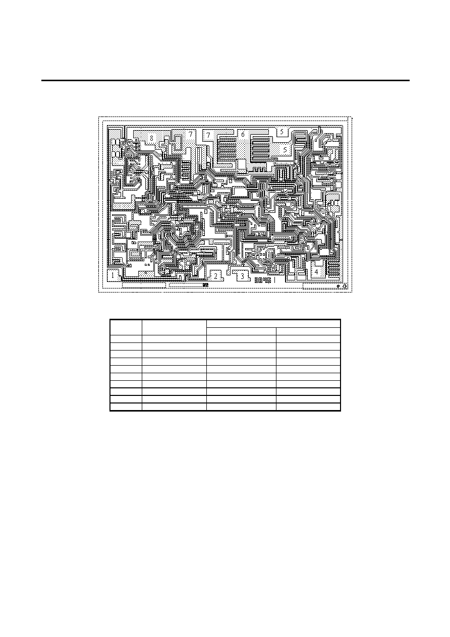
Pad location MIK3842A/43A/44A/45A
Chip size: 2.38 x 1.63 mm
Pad Location Coordinates
Coordinates µm
Pad N
Pad Name
X Y
1 COMP
90
110
2 V
FB
1050
110
3 I
SENSE
1310
110
4 R
T
/C
T
2000
150
5 POWER
GND
1700
1280
6 GND
1680
1450
7 OUT
1310
1410
8 POWER
V
CC
990 1410
9 V
CC
815
1410
10 V
REF
460
1390
Page 8 of 8