1
MIK393
∑
LOW POWER LOW OFFSET VOLTAGE DUAL COMPARATORS
MI
K
R
ON J
S
C
∑
ht
t
p
://www.m
i
k
r
o
n
.r
u
∑
M
a
rc
h 2003
CONTENTS
Page
GENERAL DESCRIPTION
1
FEATURES
1
SCHEMATIC DIAGRAM
2
PIN CONNECTIONS
2
ABSOLUTE MAXIMUM RATINGS
2
SWITCHING CHARACTERISTICS
2
ELECTRICAL CHARACTERISTICS
3
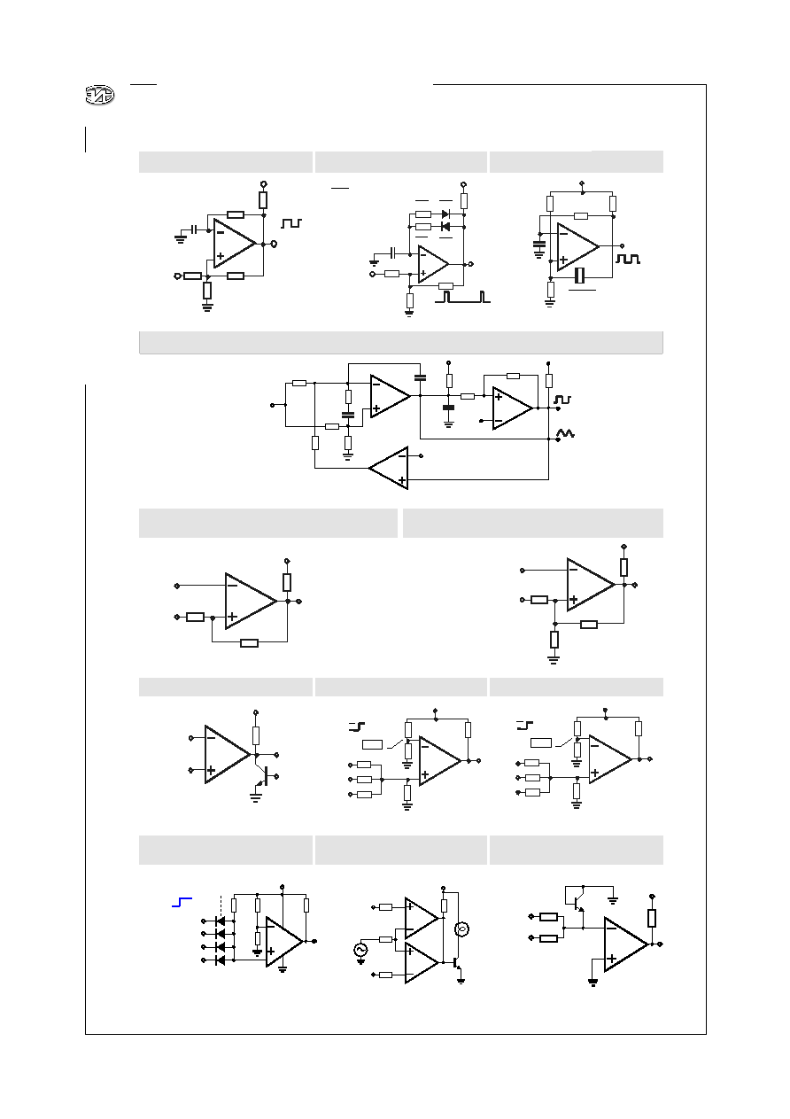
TYPICAL APPLICATIONS
3
Basic Comparator
3
Driving CMOS
3
Driving TTL
3
Square-wave Oscillator
4
Pulse Generator
4
Crystal Controlled Oscillator
4
Two-Decade High Frequency VCO
4
Non-Inverting Comparator with Hysteresis
4
Inverting Comparator with Hysteresis
4
Output Strobing
4
AND Gate
4
OR Gate
4
Large Fan-in AND Gate
4
Limit Comparator
4
CONTENTS
Page
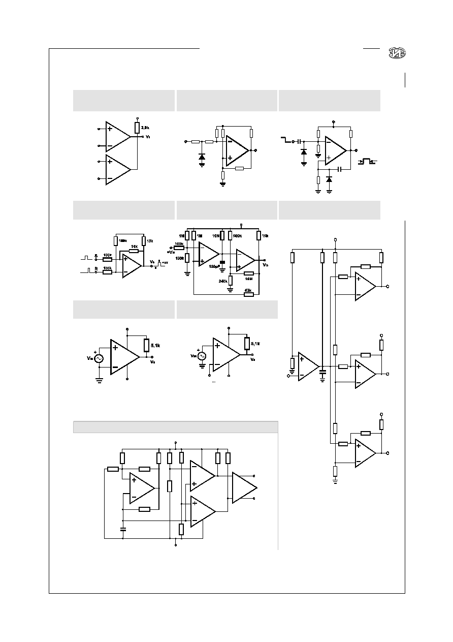
Comparing Input Voltages of Opposite
Polarity
4
ORing the Outputs
5
Zero Crossing Detector (Single Power
Supply)
5
One-Shot Multivibrator
5
Bi-Stable Multivibrator
5
One-Shot Multivibrator with Input Lock
Out
5
Time Delay Generator
5
Zero Crossing Detector
5
Comparator With a Negative Reference
5
SPLIT-SUPPLY APPLICATIONS
5
MOS Clock Driver
5
TYPICAL PERFORMANCE CHARACTERISTICS
6
Supply Current
6
Input Current
6
Low Level Output Voltage
6
Response Time for Various Input
Overdrives--Positive Transition
6
Response Time for Various Input
Overdrives--Negative Transition
6
PHYSICAL DIMENSIONS AND MARKING
DIAGRAMS
7
SOP≠8 Package & Marking Diagram
7
DIP≠8 Package & Marking Diagram
7
ORDERING INFORMATION
8
GENERAL DESCRIPTION
The MIK393 consists of two independent precision
voltage comparators which were designed specifically
to operate from a single power supply over a wide
range of voltages. Operation from split power
supplies is also possible and the low power supply
current drain is independent of the magnitude of the
power supply voltage. These comparators also have a
unique characteristic in that the input common-mode
voltage range includes ground, even though operated
from a single power supply voltage.
Application areas include limit comparators, simple
analog to digital converters; pulse, squarewave and
time delay generators; wide range VCO; MOS clock
timers; multivibrators and high voltage digital logic
gates. The MIK393 series was designed to directly
interface with TTL and CMOS. When operated from
both plus and minus power supplies, the MIK393 series
will directly interface with MOS logic where their low
power drain is a distinct advantage over standard
comparators.
FEATURES
∑
Wide supply voltage range 2.0V to 32V.
∑
Low supply current drain independent of supply
voltage.
∑
Low input biasing current: 25 nA typ.
∑
Low input offset current: 5 nA typ.
∑
Low input offset voltage: 2 mV typ.
∑
Input common-mode voltage range includes GND.
∑
Differential input voltage range equal to the
power supply voltage.
∑
Low output saturation voltage.
∑
Output voltage compatible with TTL, MOS and
CMOS logic.
MIK393
LOW POWER LOW OFFSET VOLTAGE DUAL COMPARATORS
DATA SHEET
M
ARCH
2003
N
O
. 00003
R
EV
. 1-03
REPLACEMENT
of
LM393

2
LOW POWER LOW OFFSET VOLTAGE DUAL COMPARATORS
∑
MIK393
Design by Vladimir F.Lityaghin / E-mail: lityaghin@mail.ru / Tel: +7(095)532-64-54
MI
K
R
ON J
S
C
∑
ht
t
p
://www.m
i
k
r
o
n
.r
u
∑
M
a
rc
h 2003
SCHEMATIC DIAGRAM
(Ω MIK393)
PIN CONNECTIONS
(top view)
MIK393N
DIP-8
SOP-8
MIK393M
1
2
1_OUT
1_IN
--
Vcc
2_OUT
2_IN
--
2_IN
+
1_IN
+
GND
*
C
L
includes probe and jig capacitance.
NOTE 1
: The response time specified is the interval between the input step function and the instant when the output
crosses 1.4V.
SWITCHING CHARACTERISTICS
V
cc
=5V;
A
=25∞C
PARAMETER
TEST CONDITIONS
MIN TYP MAX UNIT
100-mV input step with
5-mV overdrive
1.3
Response
time
R
L
connected to 5V through 5.1 k
;
C
L
=15pF* (See Note1)
TTL-level input step
0.3
µs
OUTPUT
Vcc
GND
NONINVERTING
INPUT
INVERTING
INPUT
ABSOLUTE MAXIMUM RATINGS
NOTE 1: For operating at high temperatures, the MIK393 must be derated based on a 125∞C maximum junction
temperature and a thermal resistance of 170∞C/W which applies for the device soldered in a printed circuit
board, operating in a still air ambient. The low bias dissipation and the "ON-OFF" characteristic of the
outputs keeps the chip dissipation very small (P
D
100 mW), provided the output transistors are allowed to
saturate.
PARAMETER
VALUE
UNIT
DIFFERENTIAL INPUT VOLTAGE
36
_
V
INPUT VOLTAGE
-0,3
˜
+36
_
V
INPUT CURRENT
20
_
mA
POWER DISSIPATION
(Note 1)
Molded DIP
780
mW
Small Outline Package
510
mW
OUTPUT SHORT-CIRCUIT TO GROUND
Continuous
OPERATING TEMPERATURE RANGE
0 to +70
_
∞C
STORAGE TEMPERATURE RANGE
-65 to +150
∞C
SYMBOL
V
IDR
V
IN
I
O
I
OS
T
A
Tstg
Vcc
SUPPLY VOLTAGE
36
_
V
3
MIK393
∑
LOW POWER LOW OFFSET VOLTAGE DUAL COMPARATORS
MI
K
R
ON J
S
C
∑
ht
t
p
://www.m
i
k
r
o
n
.r
u
∑
M
a
rc
h 2003
BASIC COMPARATOR
DRIVING CMOS
DRIVING TTL
TYPICAL APPLICATIONS
(Vcc = 5 V)
+V
in
3,0k
+V
REF
V
0
V+
1/2 MIK393
These dual comparators feature high gain, wide
bandwidth characteristics. This gives the device
oscillation tendencies if the outputs are
capacitively coupled to the inputs via stray
capacitance. This oscillation manifests itself during
output transitions (V
OL
to V
OH
). To alleviate this
situation, input resistors <10 k
should be used.
The addition of positive feedback (<10 mV) is also
recommended. It is good design practice to ground
all unused pins.
Differential input voltages may be larger than
supply voltage without damaging the comparator's
inputs. Voltages more negative than ≠0.3 V should
not be used.
10k
1/4 MM54CXX
+5,0 V
DC
MIK393
+5,0 V
DC
1/4 MM54CXX
100k
1/2 MIK393
Vcc
Vcc=5V
CD40XX
Vcc=5V
SN74LSXX
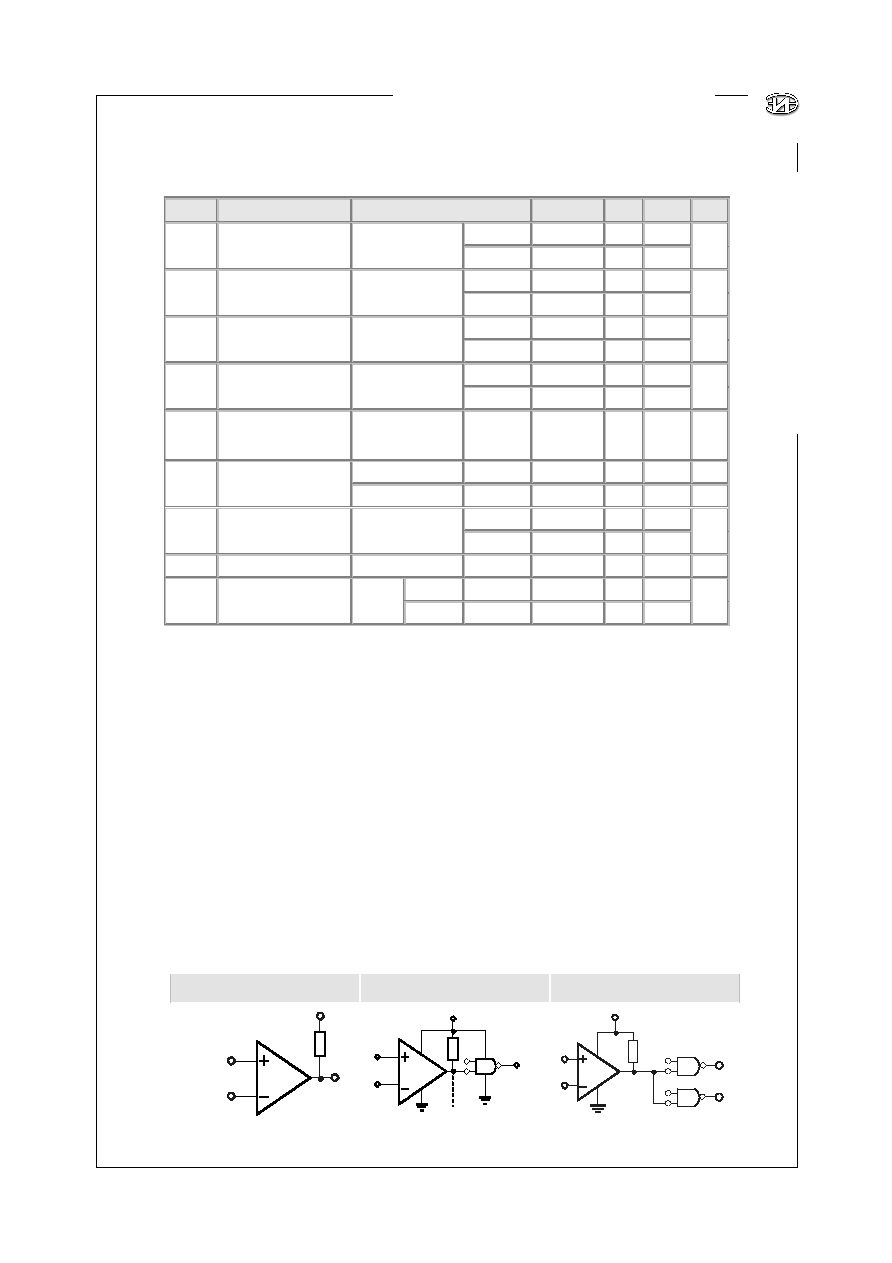
ELECTRICAL CHARACTERISTICS
electrical characteristics at specified free-air temperature, Vcc = 5 V (unless otherwise noted)
* Full range (MIN to MAX), for the MIK393 is 0∫C to 70∫C. All characteristics are measured with zero common-mode
input voltage unless otherwise specified.
** The voltage at either input or common-mode should not be allowed to go negative by more than 0.3V. The upper
end of the common-mode voltage range is VCC -1.5V, but either or both inputs can go to 30V without damage.
SYMBOL
PARAMETER
TEST CONDITIONS*
MIN
TYP
MAX UNIT
25
∞
C
2.0 5.0
V
IO
Input offset voltage
Vcc
= 5V to 30V;
V
IC
=
V
ICR
min;
Vo
= 1.4
Full range
9.0
mV
25
∞
C
5.0 50.0
l
IO
Input offset current
Vo
= 1.4V
Full range
150.0
nA
25
∞
C
-25.0 -250.0
I
IB
Input bias current
Vo
= 1.4V
Full range
-400.0
nA
25
∞
C 0 to Vcc -1.5
V
ICR
Common-mode input
voltage range**
Full range 0 to Vcc -2.0
V
A
VD
Large-signal differential
voltage amplification
Vcc
= 15 V;
Vo
=1.4V to 11.4 V;
R
L
15 k
t
O
V
CC
25
∞
C
50.0 200.0
V/mV
V
OH
= 5 V;
V
ID
= 1V
25
∞
C
0.1 50.0
nA
l
OH
High-level output current
V
OH
= 30V;
V
ID
= 1V Full range
1.0 µA
25
∞
C
150.0 400.0
V
OL
Low-level output voltage
I
OL
= 4 mA;
V
ID
= -1V
Full range
700.0
mV
l
OL
Low-level output current
V
OL
= 1.5V;
V
ID
= -1V
25
∞
C
6.0
mA
V
CC
= 5V
25
∞
C
0.8 1.0
I
CC
Supply current
R
L
=
V
CC
= 30V Full range
2.5
mA