
Replacement of
XC62GR/GP-XX
MIK62GR/GP-XX
150 mA Low Dropout
Regulator
Preliminary July 2001
Description
The MIK62G series is a group of positive voltage output, three-pin regulators, that provide a high current even when the input/output
voltage differential is small. Low power consumption and high accuracy is achieved through CMOS and programmable fuse
technologies. Output voltage: 2.0V to 6.0V. The MIK62G consists of a high-precision voltage reference, an error correction circuit, and a
current limited output driver. Transient response to load variations have improved in comparison to the existing series. With good
transient responses, output remains stable even during load changes. The CE input enables the output to be turned off, resulting in
reduced power consumption. SOT-25 (150mW) and SOT-89-5 (500mW) packages are available. With regards to the CE function, as
well as the positive logic MIK62GR series, a negative logic MIK62GP series is also available.
Features
∑
Maximum output current 150mA
∑
Highly accurate: Output voltage +/- 2%
∑
Low power consumption.
∑
Small input/output differential: 0.38V at 160mA
Applications
∑ Battery-powered Equipment
∑ Voltage supplies for cellular phones
∑ Portable Cameras and Video Recorders
∑ Reference Voltage Sources
∑ Palmtops
Absolute Maximum Ratings
Symbol Parameter
Maximum
Units
Vin
Input Voltage
12
V
Iout Output
Current
500
mA
Vce
CE Input Voltage
Vss-0.3~Vin+0.3
Vout Output
Voltage
Vss-0.3~Vin+0.3
V
Pd
Continuous Total Power Dissipation
SOT-25
SOT-89-5
150
500
mW
Topr
Operating Ambient Temperature
-30 ~ +80
∞C
Tstg
Storage temperature
-40 ~ +125
∞C
Pin Configuration
Functions
Series CE Voltage
Output
MIK62GR-XX H
L
ON
OFF
MIK62GP-XX H
L
OFF
ON
Page 1 of 2
Replacement of
XC62GR/GP-XX
MIK62GR/GP-XX
150 mA Low Dropout
Regulator
Preliminary July 2001
Electrical Characteristics
(at T
a
= 25
o
C, V
IN
= Vout(nominal)+1V; unless otherwise noted)
Parameter Conditions
Min
Typ Max Units
Output Voltage Accuracy
Io
=40mA
-2%
+2%
V
Line Regulation
Vout/VinVout
Io=40mA, (Vout+1V)<Vin<10V
0.2
0.3
%/V
Load Regulation
Vin=Vout+1V, 1mA
Io
80mA
Cout=1
µF
0,04
%/mA
Maximum Output Current
150
mA
Current Limit
1000
mA
Ground Pin Current 1
Ground Pin Current 2
Vin=Vce=Vout+1V
Vin=Vout+1V Vce=Vss
19
0,1
µA
CE Input Voltage "High"
1,5
V
CE Input Voltage "Low"
0,25
V
CE Input Current "High"
Vce=Vin
1
µkA
CE Input Current "Low"
Vce=Vss
-0,2
-0,05
0
µkA
Dropout Voltage
Io=80mA
Io=160mA
200
380
395
770
mV
Output Voltage Temperature Characteristics
Iout=10mA -30
Topr80∞
±100
ppm/
∞C
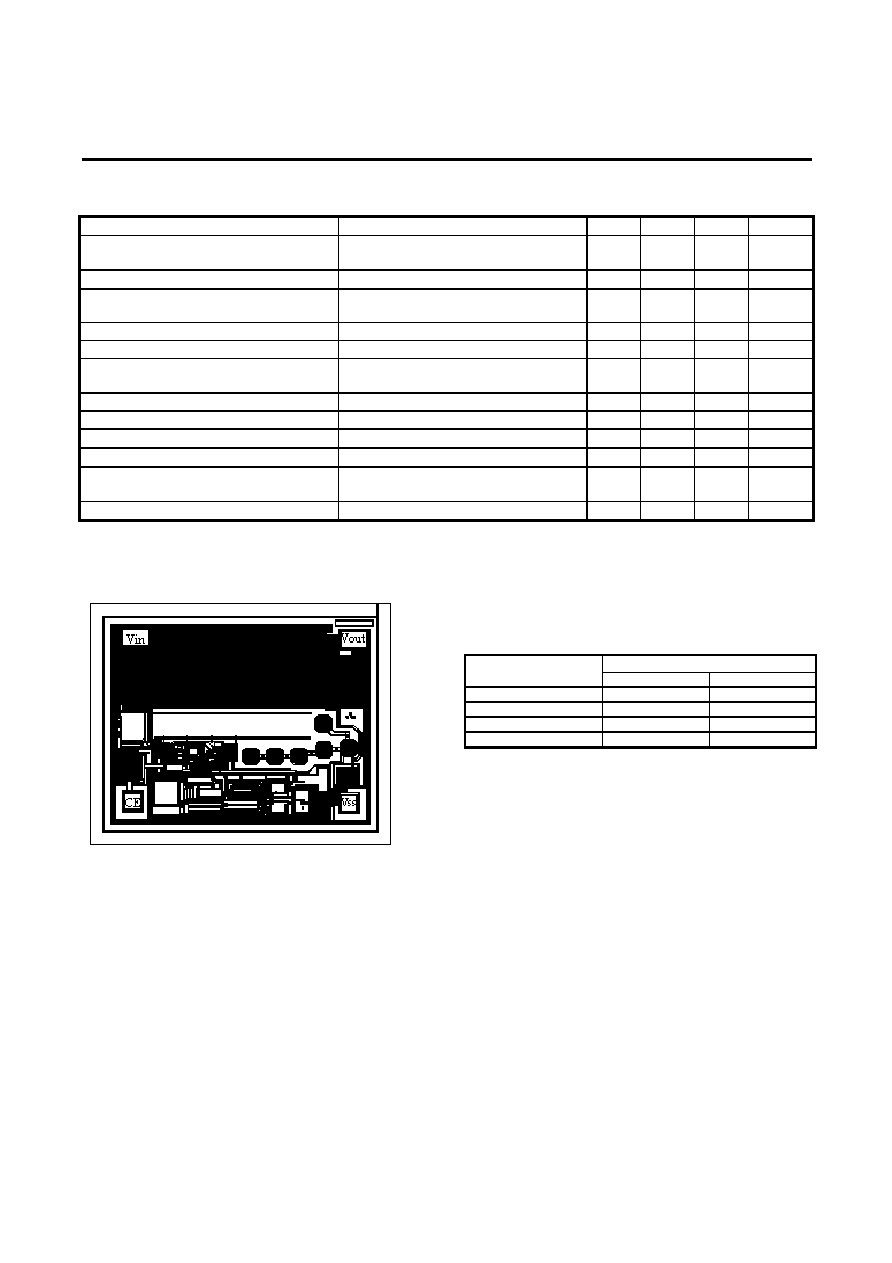
Pad location
Chip size: 1.48 * 1.18 mm
Pad Location Coordinates
(the center of pads)
Coordinates (
µm)
Pad Name
X Y
Vout 1235
966
Vce 172
173
Vin 159,5
977
Vss 1235
165.5
Page 2 of 2