MIK7024K-XX
32 KHz Standard Watch Circuit
with Alarm In
January 2002
Features
∑ Single 1.5 V battery operation
∑ High precision 32.768 KHz crystal controlled oscillator
∑ Low power consumption
∑ Active-low alarm input
∑ VSEM input for selection of SECONDA-mode without additional mask and bonding by means of external Vss bonding to this pad
instead of Vss pad
∑ Mask option for:
-
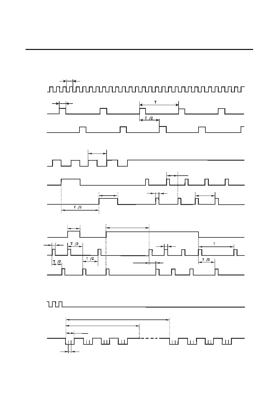
Integrated capacitors CI, CO=1pF+2pF+3pF+5pF+10pF=21pF max
-
motor period T
M
= 2, 4 ,6, 8, 10, 12, 20, 24, 30, 40, 60, or 120 sec (for VSEM input is open)
-
motor pulse width t
M
= 15.625 to 125 msec in increments of 15.625 msec
-
INC motor increment button input to advance by
∑ One step at press duration less 2 seconds
∑ Multiple increments at press duration more 2 sec with frequency 8 Hz or 16 Hz
-
Alarm drive current I
OL
, I
H
> 200mkA for push-pull output or I
OL
> 50mA for open drain output
-
2 KHz or 4 KHz modulated by 8 Hz and 1 Hz alarm output
Electrical Characteristics
(V
DD
= 1.5 V, V
SS
= 0 V; T
a
= 25
o
C, unless otherwise specified)
Parameters Symbol Test
conditions Min
Typ
Max
Units
Operating Voltage
V
DD
1.2
1.5
1.8
V
Operating Current
I
DD
Without
Load
2.0 mkA
I
OL
V
DD
= 1.5V, V
OL
=1.1V
50
≠
≠
mA
Alarm Current (NALO)
- Open Drain Output
- Push-Pull Output
|I
OLH
| V
DD
= 1.2V, V
OL
=0.6V
200
≠
≠
mkA
|I
M
|
R
L
= 200, V
DD
= 1.2V
4.0
≠
≠
mA
Motor Outputs:
-Drive Current
-Motor Cycle Time
-Motor Pulse Width
-Motor Fast Advance
Frequency
T
M
t
M
F
INC
sec
msec
Hz
-Alarm Frequency
F
ALA
Verification
at FC
KHz
Oscillator:
-Input Capacitance
-Output Capacitance
CI
CO
See Option List
pF
-Stability
F/F
V
DD
=1.2B ≠ 1.8B
CI=CO=25pF
≠
≠
3.0
ppm
-Start-up Voltage
V
ST
Within 2 sec
≠
≠
1.2
V
* Quartz Crystal Parameters:
Frequency Fp =32768 Hz, Load capacitance C
L
= 12.5 pF,
Static capacitance C0 = 1.2 pF, Dynamic capacitance C1 = 3.0 fF,
Series resistance R
S
= 35 K
Option List
T
M
(sec)
Number
IC
VSEM
open
VSEM
Low
t
M
(msec)
F
ALA
(KHz)
F
INC
(Hz)
NALO
Output
Type
CI
(pF)
CO
(pF)
7024K ≠ 01
120
2
31.25
2
8
Open Drain
2
2
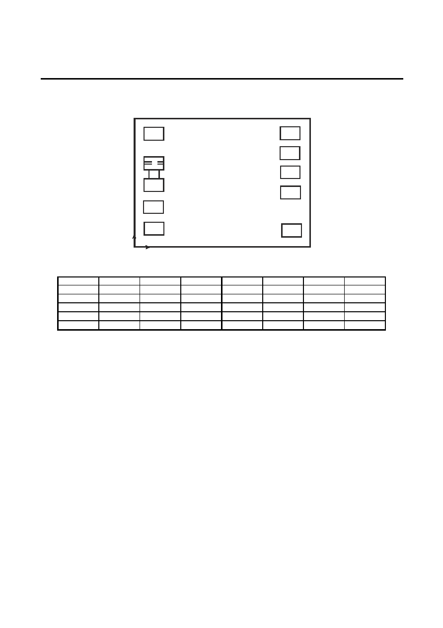
Pin Description
Pad N
0
Pad Name
Description
Pad N
0
Pad
Name
Description
1
OO
Oscillator Output
6
MOT2
Motor Drive Output 2
2
VSEM
Negativ Power Supply-SEC-
Mode/MIN-Mode input
7 NALO
Alarm
Output
3 V
SS
Negative Power Supply
8
INC
Increment Input
4 NALI
Alarm/Test
Input/Output
9 V
DD
Positive Power Supply
5
MOT1
Motor Drive Output 1
10
OI
Oscillator Input
Page 1 of 4