500-6000 MHz
Dual, Ultra Low Noise, High IP3 Amplifier
Page 1 of 14
Mimix Broadband, Inc., 10795 Rockley Rd., Houston, Texas 77099
Tel: 281.988.4600 Fax: 281.988.4615 mimixbroadband.com
Characteristic Data and Specifications are subject to change without notice.
©2006 Mimix Broadband, Inc.
Export of this item may require appropriate export licensing from the U.S. Government. In purchasing these parts, U.S. Domestic customers accept
their obligation to be compliant with U.S. Export Laws.
CDQ0303-QS
May 2006 - Rev 24-May-06
Features
Applications
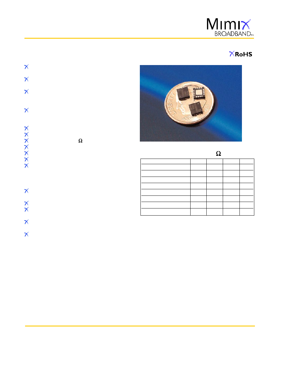
Typical Specifications (50 System)
Description
Matched Pair of Transistors for Optimum
Balanced Amplifier Design
AlGaAs/InGaAs/AlGaAs Pseudomorphic High
Electron Mobility Transistor (pHEMT)
High Gain:
25 dB @ 900 MHz
21 dB @ 1900 MHz
Low Noise Figure:
0.6 dB @ 900 MHz
0.7 dB @ 1900 MHz
17 dBm P1dB at 2 GHz
33 dBm OIP3 at 2 GHz
600µm Gate Width: 50 Output Impedance
Excellent Uniformity
Ultra Compact Surface-Mount QFN Package
10 Year MTBF Lifetime
RoHS-Compliant Construction
Low Noise Amplifiers and Oscillators Operating
over the RF and Microwave Frequency Ranges
Cellular/PCS/GSM/W-CDMA
Mobile Handsets, Base Station Receivers and
Tower-Mount Amplifiers
WiMAX WLAN, LEO, GEO, WLL/RLL, GPS and
MMDS Applications
General Purpose Discrete pHEMT for Other Ultra
Low-Noise and Medium Power Applications
Parameter
900 MHz
1900 MHz 2400 MHz
Units
S21 Gain
23.5
20.0
16.0
dB
S11 Input Return Loss
-3.0
-4.0
-3.0
dB
S22 Output Return Loss
-3.5
-4.5
-7.0
dB
Output IP3
31.8
32.5
32.7
dBm
Output P1 dB
16.5
16.0
16.0
dBm
Noise FIgure
0.55
0.72
0.89
dB
Operating Current Range
50
50
50
mA
Supply Voltage
3.0
3.0
3.0
V
Note: Typical specifications represents performance for each side of
the matched pair of transistors in the recommended application circuit
board (see page 15). It is anticipated that the pair will be used in a bal-
anced circuit configuration, hence the matches are optimized for best
noise figure and OIP3 performance.
The CDQ0303-QS is a dual, ultra low-noise amplifi-
er combining high gain, state-of-the-art noise figure and high
IP3. Utilizing Mimix's distinctive in-house GaAs fabrica-
tion advantage and matched pair technology, co-located
matched transistor die are assembled in the 4mm x 4mm
QFN package. The low-cost, surface-mount, 16 terminal,
plastic package is also lead-free.
Packaging a matched pair of ultra low-noise devices
in a single package makes the CDQ0303-QS an ideal product
for balanced amplifier implementation. It is intended for
many applications operating in the 900 MHz to 2400 MHz
frequency range. It can also be used in a dual-band configu-
ration where a single transistor is used for each band.
Mimix's high performance packaged pHEMTs are
ideal for use in all applications where low-noise figure, high
gain, medium power and good intercept is required. The
CDQ0303-QS is the perfect solution for the first or second
stage of a base station LNA due to the excellent combination
of low-noise figure and linearity. It is also well suited as a
medium power driver stage in pole-top amplifiers and other
transmit functions, particularly as the low thermal resistance
allows extended power dissipation when voltage and current
are adjusted for increased power and linearity.

Parameters
Test Conditions
Min
Typ
Max
Units
Operating Frequency
500
3000
MHz
DC Supply Voltage
Vdd Only
3
V
Saturated Drain Current (Per Device)
Vds=4.5V, Vgs=0V
120
165
200
mA
Idd (Per Device)
Vgg=-0.65 nom
60
mA
Transconductance (Per Device)
Vds=4.5V. Gm=Idss/Vp
190
250
mmho
Associated Gain 1
f=900 MHz
Vd=3V, Ids=50 mA
23
25
dB
f=1900 MHz
Vd=3V, Ids=50 mA
18
20
dB
Noise Figure 1
f=900 MHz
Vd=3V, Ids=50 mA
0.6
dB
f=1900 MHz
Vd=3V, Ids=50 mA
0.7
dB
Output Third Order Intercept Point 1
f=900 MHz
Vd=3V, Ids=50 mA
29
dBm
f=1950 MHz
Vd=3V, Ids=50 mA
29
dBm
Isolation (Between IN1 and IN2)
f=900 MHz
Vd=3V, Ids=50 mA
34
dB
f=1950 MHz
Vd=3V, Ids=50 mA
29
dB
Input Overdrive Tollerance Level
Returns to full operation after 1 min.
17
dBm
ESD (ESD precautions should be followed)
ESD (HBM) for (All I/Os)
600
V
500-6000 MHz
Dual, Ultra Low Noise, High IP3 Amplifier
Page 2 of 14
CDQ0303-QS
Parameter
Rating
Parameter
Rating
Parameter
Rating
Drain-Source Voltage 2
+5.5 V
Drain Current 2
Idss 3 A
Channel Temperature
+175∫C
Gate-Source Voltage 2
-5.0 V
Total Pwr Dissipation
1.12 W
Storage Temperature
-65∫C to +160∫C
Gate-Drain Voltage 2
-5.0 V
RF Input Power
17 dBm
Thermal Resistance
70∫C/W
Notes:
1. Operation of this device above any one of these parameters may cause permanent damage
2. Assumes DC quiescent conditions. RF OFF.
3. Vgs=0V
Ta=25∫C, Typical device RF parameters measured in test system.
Notes:
1. Measured in Celeritek Evaluation Board (No circuit de-embedding used). See page 15.
Pin Out Detail
Pin
Function
Description
16
IN 1
Amplifier 1 RF Input
13
IN 2
Amplifier 2 RF Input
5
OUT 1
Amplifier 1 RF Output
8
OUT 2
Amplifier 2 RF Output
1, 2, 3, 4
VS 1
Amplifier 1 Source Connection
9, 10, 11, 12
VS 2
Amplifier 2 Source Connection
6, 7, 14, 15
GND
Main Heat-Sinking Connection
VS 1 1
VS 1 2
VS 1 3
VS 1 4
12 VS 2
11 VS 2
10 VS 2
9 VS 2
OUT 1
5
VS 1
6
VS 2
7
OUT 2
8
16
IN 1
15
VS 1
14
VS 2
13
IN 2
Mimix Broadband, Inc., 10795 Rockley Rd., Houston, Texas 77099
Tel: 281.988.4600 Fax: 281.988.4615 mimixbroadband.com
Characteristic Data and Specifications are subject to change without notice.
©2006 Mimix Broadband, Inc.
Export of this item may require appropriate export licensing from the U.S. Government. In purchasing these parts, U.S. Domestic customers accept
their obligation to be compliant with U.S. Export Laws.
May 2006 - Rev 24-May-06
Electrical Characteristics
Functional Block Diagram
Absolute Maximum Ratings
1

500-6000 MHz
Dual, Ultra Low Noise, High IP3 Amplifier
Page 3 of 14
CDQ0303-QS
Mimix Broadband, Inc., 10795 Rockley Rd., Houston, Texas 77099
Tel: 281.988.4600 Fax: 281.988.4615 mimixbroadband.com
Characteristic Data and Specifications are subject to change without notice.
©2006 Mimix Broadband, Inc.
Export of this item may require appropriate export licensing from the U.S. Government. In purchasing these parts, U.S. Domestic customers accept
their obligation to be compliant with U.S. Export Laws.
May 2006 - Rev 24-May-06
Typical Pulsed I-V Performance

500-6000 MHz
Dual, Ultra Low Noise, High IP3 Amplifier
Page 4 of 14
CDQ0303-QS
Mimix Broadband, Inc., 10795 Rockley Rd., Houston, Texas 77099
Tel: 281.988.4600 Fax: 281.988.4615 mimixbroadband.com
Characteristic Data and Specifications are subject to change without notice.
©2006 Mimix Broadband, Inc.
Export of this item may require appropriate export licensing from the U.S. Government. In purchasing these parts, U.S. Domestic customers accept
their obligation to be compliant with U.S. Export Laws.
May 2006 - Rev 24-May-06
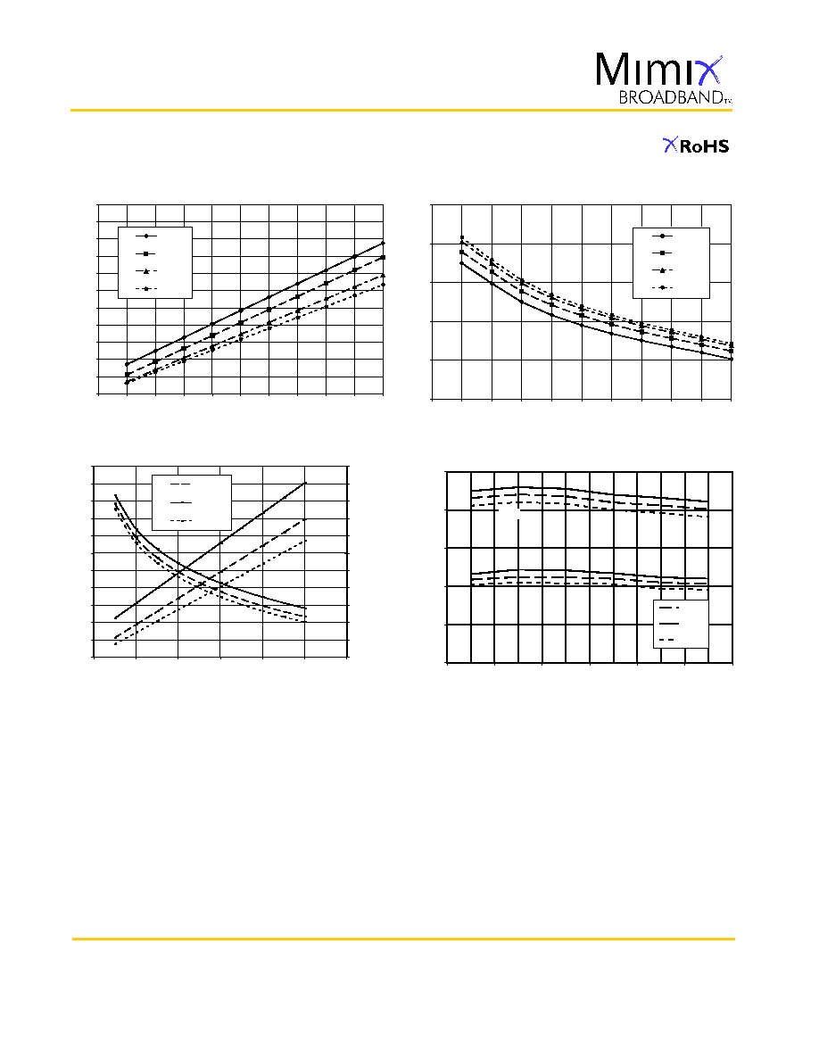
Typical Performance
NF and Ga vs. Bias at 1GHz
0
0.15
0.3
0.45
0.6
0.75
0.9
1.05
1.2
1.35
1.5
1.65
0
10
20
30
40
50
60
70
IDSQ(mA)
NFmin(dB)
7
8.5
10
11.5
13
14.5
16
17.5
19
20.5
22
23.5
Ga(dB)
3V
2V
4V
Ga
NFmin
NF and Ga vs. Bias at 2GHz
0
0.15
0.3
0.45
0.6
0.75
0.9
1.05
1.2
1.35
1.5
1.65
0
10
20
30
40
50
60
70
IDSQ(mA)
NFmin(dB)
5
6.5
8
9.5
11
12.5
14
15.5
17
18.5
20
21.5
Ga(dB)
3V
2V
4V
Ga
NFmin
OIP3 and P
1dB
vs. Bias at 2GHz
0
5
10
15
20
25
30
35
0
10
20
30
40
50
60
I
DSQ
(mA)
OIP3, P
1dB
(dBm)
4V
3V
2V
OIP3
P
1dB
OIP3 and P
1dB
vs. I
DSQ
at 1GHz
0
5
10
15
20
25
30
35
0
10
20
30
40
50
60
I
DSQ
(mA)
OIP3, P
1dB
(dBm)
4V
3V
2V
OIP3
P
1dB
1,2
1,2
2
2
Notes:
1. P1dB and OIP3 measurements are performed with passive biasing. Idsq is set with zero RF drive applied. As P1dB is approached, the drain current may
increase or decrease depending on frequency and DC bias point. At lower values of Idsq the device is running in a Class AB mode and current tends to rise
as P1dB is approached. As an example, at a Vds = 3.0V and Idsq = 10 mA, Id increases to 30 mA as P1dB of 16.5 is approached. This rise in current is no
longer present as Idsq approaches 60 mA.
2. Measurements made on a fixed tuned test system set for optimum noise match. Circuit losses have been de-embedded for the actual measurements.
500-6000 MHz
Dual, Ultra Low Noise, High IP3 Amplifier
Page 5 of 14
CDQ0303-QS
Mimix Broadband, Inc., 10795 Rockley Rd., Houston, Texas 77099
Tel: 281.988.4600 Fax: 281.988.4615 mimixbroadband.com
Characteristic Data and Specifications are subject to change without notice.
©2006 Mimix Broadband, Inc.
Export of this item may require appropriate export licensing from the U.S. Government. In purchasing these parts, U.S. Domestic customers accept
their obligation to be compliant with U.S. Export Laws.
May 2006 - Rev 24-May-06
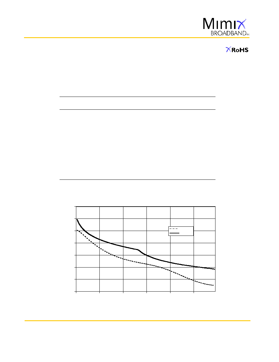
Typical Performance
Nfmin vs. Frequency and Current, Vd=3V
0
0.15
0.3
0.45
0.6
0.75
0.9
1.05
1.2
1.35
1.5
1.65
0
1
2
3
4
5
6
7
8
9
10
Frequency (GHz)
NFmin (dB)
10mA
20mA
40mA
60mA
Associated Gain vs. Frequency and Current Vd=3V
0
5
10
15
20
25
0
1
2
3
4
5
6
7
8
9
10
Frequency (GHz)
Ga (dB)
10mA
20mA
40mA
60mA
Nfmin and Associated Gain vs. Frequency and Temperature @ Vd=3V,Id=20mA
2
4
6
8
10
12
14
16
18
20
22
24
0
2
4
6
8
10
12
Frequency (GHz)
Ga (dB)
0
0.15
0.3
0.45
0.6
0.75
0.9
1.05
1.2
1.35
1.5
1.65
NFmin (dB)
25deg
-40deg
80deg
NFmin
Ga
OIP3 and P1dB vs. Frequency and Temperature, Vds=3V, Ids=20mA
5
10
15
20
25
30
1
2
3
4
5
6
Frequency (GHz)
OIP3, P1dB (dBm)
25deg
-40deg
85deg
OIP3
P
1dB
2
2
1
1,2
Notes:
1. P1dB and OIP3 measurements are performed with passive biasing. Idsq is set with zero RF drive applied. As P1dB is approached, the drain current may
increase or decrease depending on frequency and DC bias point. At lower values of Idsq the device is running in a Class AB mode and current tends to rise
as P1dB is approached. As an example, at a Vds = 3.0V and Idsq = 10 mA, Id increases to 30 mA as P1dB of 16.5 is approached. This rise in current is no
longer present as Idsq approaches 60 mA.
2. Measurements made on a fixed tuned test system set for optimum noise match. Circuit losses have been de-embedded for the actual measurements.

500-6000 MHz
Dual, Ultra Low Noise, High IP3 Amplifier
Page 6 of 14
CDQ0303-QS
Mimix Broadband, Inc., 10795 Rockley Rd., Houston, Texas 77099
Tel: 281.988.4600 Fax: 281.988.4615 mimixbroadband.com
Characteristic Data and Specifications are subject to change without notice.
©2006 Mimix Broadband, Inc.
Export of this item may require appropriate export licensing from the U.S. Government. In purchasing these parts, U.S. Domestic customers accept
their obligation to be compliant with U.S. Export Laws.
May 2006 - Rev 24-May-06
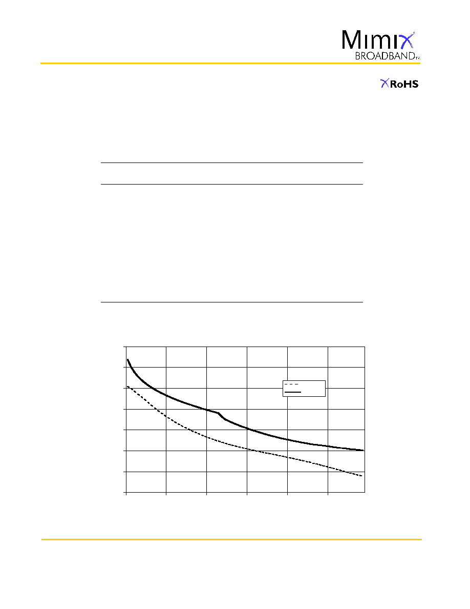
Typical Noise Parameters
S-Parameter Data Files are available on-line at: www.mimixbroadband.com
Freq.
NFmin
Gamma Opt
Rn
Ga
GHz
db
Mag.
Ang.
db
1.0
0.19
0.83
30.97
0.44
17.51
2.0
0.34
0.74
56.07
0.41
14.90
3.0
0.49
0.66
77.32
0.52
12.51
4.0
0.64
0.57
96.15
0.69
10.82
5.0
0.78
0.50
114.83
0.26
9.52
6.0
0.92
0.44
135.28
0.11
8.45
7.0
1.04
0.38
159.59
0.07
7.55
8.0
1.14
0.37
-173.41
0.08
6.78
9.0
1.23
0.40
-149.74
0.13
6.01
10.0
1.29
0.46
-133.22
0.23
5.18
CDQ0303-QS Typical Noise Parameters
(Vds = +3.0V, Ids = 10 mA)
MSG.MAG and |S
21
|
2
vs. Frequency at 3V, 10mA
-10.00
-5.00
0.00
5.00
10.00
15.00
20.00
25.00
0.50
3.50
6.50
9.50
12.50
15.50
Frequency (GHz)
MSG/MAG and S
21
(dB)
S21
MSG/MAG
500-6000 MHz
Dual, Ultra Low Noise, High IP3 Amplifier
Page 7 of 14
CDQ0303-QS
Mimix Broadband, Inc., 10795 Rockley Rd., Houston, Texas 77099
Tel: 281.988.4600 Fax: 281.988.4615 mimixbroadband.com
Characteristic Data and Specifications are subject to change without notice.
©2006 Mimix Broadband, Inc.
Export of this item may require appropriate export licensing from the U.S. Government. In purchasing these parts, U.S. Domestic customers accept
their obligation to be compliant with U.S. Export Laws.
May 2006 - Rev 24-May-06
Typical Noise Parameters
Freq.
NFmin
Gamma Opt
Rn
Ga
GHz
db
Mag.
Ang.
db
1.0
0.15
0.83
22.26
0.23
18.93
2.0
0.26
0.72
59.00
0.24
16.38
3.0
0.38
0.59
88.09
0.40
13.92
4.0
0.50
0.49
112.62
0.33
12.14
5.0
0.63
0.40
135.17
0.10
10.78
6.0
0.76
0.33
157.85
0.06
9.64
7.0
0.88
0.29
-178.05
0.07
8.67
8.0
1.00
0.29
-157.41
0.08
7.85
9.0
1.10
0.34
-145.46
0.10
7.02
10.0
1.21
0.41
-142.31
0.12
6.19
CDQ0303-QS Typical Noise Parameters
(Vds = +3.0V, Ids = 20 mA)
MSG.MAG and |S
21
|
2
vs. Frequency at 3V, 20mA
-5.00
0.00
5.00
10.00
15.00
20.00
25.00
30.00
0.50
3.50
6.50
9.50
12.50
15.50
Frequency (GHz)
MSG/MAG and S
21
(dB)
S21
MSG/MAG
S-Parameter Data Files are available on-line at: www.mimixbroadband.com

500-6000 MHz
Dual, Ultra Low Noise, High IP3 Amplifier
Page 8 of 14
CDQ0303-QS
Mimix Broadband, Inc., 10795 Rockley Rd., Houston, Texas 77099
Tel: 281.988.4600 Fax: 281.988.4615 mimixbroadband.com
Characteristic Data and Specifications are subject to change without notice.
©2006 Mimix Broadband, Inc.
Export of this item may require appropriate export licensing from the U.S. Government. In purchasing these parts, U.S. Domestic customers accept
their obligation to be compliant with U.S. Export Laws.
May 2006 - Rev 24-May-06
Typical Noise Parameters
Freq.
NFmin
Gamma Opt
Rn
Ga
GHz
db
Mag.
Ang.
db
1.0
0.11
0.74
23.04
0.19
20.26
2.0
0.23
0.64
61.25
0.24
17.47
3.0
0.35
0.54
91.67
0.41
14.92
4.0
0.49
0.44
117.82
0.29
13.07
5.0
0.62
0.36
142.70
0.10
11.65
6.0
0.74
0.29
169.14
0.07
10.47
7.0
0.85
0.26
-162.52
0.07
9.46
8.0
0.96
0.28
-139.75
0.09
8.60
9.0
1.06
0.33
-127.62
0.13
7.73
10.0
1.14
0.40
-124.24
0.17
6.89
CDQ0303-QS Typical Noise Parameters
(Vds = +3.0V, Ids = 40 mA)
MSG.MAG and |S
21
|
2
vs. Frequency at 3V, 40mA
-5.00
0.00
5.00
10.00
15.00
20.00
25.00
30.00
0.50
3.50
6.50
9.50
12.50
15.50
Frequency (GHz)
MSG/MAG and S
21
(dB)
S21
MSG/MAG
S-Parameter Data Files are available on-line at: www.mimixbroadband.com
500-6000 MHz
Dual, Ultra Low Noise, High IP3 Amplifier
Page 9 of 14
CDQ0303-QS
Mimix Broadband, Inc., 10795 Rockley Rd., Houston, Texas 77099
Tel: 281.988.4600 Fax: 281.988.4615 mimixbroadband.com
Characteristic Data and Specifications are subject to change without notice.
©2006 Mimix Broadband, Inc.
Export of this item may require appropriate export licensing from the U.S. Government. In purchasing these parts, U.S. Domestic customers accept
their obligation to be compliant with U.S. Export Laws.
May 2006 - Rev 24-May-06
Typical Noise Parameters
Freq.
NFmin
Gamma Opt
Rn
Ga
GHz
db
Mag.
Ang.
db
1.0
0.08
0.83
36.63
0.18
20.82
2.0
0.19
0.70
71.35
0.23
17.92
3.0
0.33
0.58
99.28
0.46
15.32
4.0
0.46
0.47
123.90
0.26
13.44
5.0
0.61
0.39
147.46
0.10
12.00
6.0
0.73
0.32
172.31
0.07
10.81
7.0
0.83
0.30
-162.17
0.08
9.79
8.0
0.94
0.32
-141.96
0.10
8.91
9.0
1.02
0.39
-131.18
0.14
8.04
10.0
1.10
0.47
-128.00
0.17
7.17
CDQ0303-QS Typical Noise Parameters
(Vds = +3.0V, Ids = 60 mA)
MSG.MAG and |S
21
|
2
vs. Frequency at 3V, 60mA
-5.00
0.00
5.00
10.00
15.00
20.00
25.00
30.00
0.50
3.50
6.50
9.50
12.50
15.50
Frequency (GHz)
MSG/MAG and S
21
(dB)
S21
MSG/MAG
S-Parameter Data Files are available on-line at: www.mimixbroadband.com

500-6000 MHz
Dual, Ultra Low Noise, High IP3 Amplifier
Page 10 of 14
CDQ0303-QS
Mimix Broadband, Inc., 10795 Rockley Rd., Houston, Texas 77099
Tel: 281.988.4600 Fax: 281.988.4615 mimixbroadband.com
Characteristic Data and Specifications are subject to change without notice.
©2006 Mimix Broadband, Inc.
Export of this item may require appropriate export licensing from the U.S. Government. In purchasing these parts, U.S. Domestic customers accept
their obligation to be compliant with U.S. Export Laws.
Typical Reflow Profiles
Reflow Profile
Ramp Up Rate
Activation Time and Temperature
Time Above Melting Point
Max Peak Temperature
Time Within 5 ∫C of Peak
Ramp Down Rate
SnPb
3-4 ∫C/sec
60-120 sec @ 140-160 ∫C
60-150 sec
240 ∫C
10-20 sec
4-6 ∫C/sec
Pb Free
3-4 ∫C/sec
60-180 sec @ 170-200 ∫C
60-150 sec
265 ∫C
10-20 sec
4-6 ∫C/sec
May 2006 - Rev 24-May-06
Die Model - Gate Width = 600 µm, Optimized for 0.1 GHz to 26.0 GHz
Cgs
1.04 pF
Rg
0.29
Cpd
0.08 pF
Cdg
0.07 pF
Ls
0.04 nH
PCG
0.195 pF
Cds
0.1 pF
Ld
0.1 nH
PCD
0.21 pF
Gm
303 mS
Lg
0.05 nH
PLS
0.085 nH
Ri
2.2 Ohm
BG
5 mil Gold wire (1 mil dia)
PLG
0.525 nH
Tau
0.06 ps
BD
5 mil Gold wire (1 mil dia)
PLD
0.55 nH
Rs
1.28
BS
3 mil Gold wire (1 mil dia)
PCDG
0.005 pF
Rd
1.35
Cpg
0.10 pF
SRL
PLG1
u uuu
u uuu
C
PCG
C
PCDG
C
PCD
SRL
PLD
WIRE
BD
WIRE
BG
uuuu
WIRE
BS
SRL
PLS
PSFET
Parker Skellern
W=600
The PSFET is a Mimix imple-
mentation of the Parker Skellern
large signal model. The model is
available as an ADS project file
on-line at: www.mimixbroadband.com
Considerations When Designing for Optimum Noise Figure Using Noise Parameters - For any two-port network, the noise figure gives a
measure of the amount of noise added to a signal transmitted through that network. In this datasheet we have given the NFmin and the
corresponding optimum source resistance values for the device under various bias conditions. NFmin represents the true minimum noise figure
when the device is presented with an impedance matching network that transforms the source impedance typically 50 ohms to that optimum
noise matching impedance reffered to as Gopt. All stability considerations still apply, of course. If the calculated Rollet stability factor (K) is less than
1, then the source and load reflection coefficients must be carefully chosen. For an accurate graphical depiction of the unstable regions, it is best
to draw stability circles.
In practice the impedance that minimizes the noise figure is different from the impedance that minimizes the return loss. Matching techniques
such as inductive feedback will be used to bring the noise match closer to this gain match. An additional inherent danger of this technique is the
increased instability of the design at higher frequencies. As the frequency increases the amount of feedback to the devices source up to an
oscillation level. This issue can be reduced by carefully choosing the input and output matching topology so that the transducer gain is limited at
the frequency of potential oscillation. Design of a high pass / los pass matching network on the input and output is one solution that addresses
this problem. Careful simulation is essential using the wideband s-parameters provided and can only be achieved through careful modeling of all
components utilized in the design, including:
1. Accurate high frequency models for all surface mount components used.
2. Accurate models of the board characteristics including loss tangents and metal thickness.
3. Use of Via holes and via pads instead of perfect grounds where used.
In any case if the reflection coefficient of the chosen matching network is other than Gopt, then the noise figure of the device will be greater than
NFmin. The losses of the matching circuits are also non-zero and it must be considered that the noise figure of the completed amplifier is equal to
the noise figure of the device plus the losses of the matching network preceding the device.
The losses of the matching networks are related to the Q of the components and associated printed circuit board loss. In general larger gate width
devices will typically have a lower Gopt as compared to smaller gate width devices. Matching to higher impedance devices requires very hi-Q
components in order to minimize circuit losses. The main reason for using smaller gate width devices is the trade-off of current consumption and
optimum noise performance. The CDQ0303-QS is a 600um gate width device has a minimum noise figure of 0.08 dB and a Gopt of Mag 0.83, Ang
36.63, making it significantly easier to match than competitive devices. Associated gain Ga is 20.82 dB.
Device Non-Linear Model - Mimix develops its own non-linear model based on its own internal device characterization. The model is verified in
different simulators and compared to the original data from which it was extracted.

500-6000 MHz
Dual, Ultra Low Noise, High IP3 Amplifier
Page 11 of 14
CDQ0303-QS
Mimix Broadband, Inc., 10795 Rockley Rd., Houston, Texas 77099
Tel: 281.988.4600 Fax: 281.988.4615 mimixbroadband.com
Characteristic Data and Specifications are subject to change without notice.
©2006 Mimix Broadband, Inc.
Export of this item may require appropriate export licensing from the U.S. Government. In purchasing these parts, U.S. Domestic customers accept
their obligation to be compliant with U.S. Export Laws.
May 2006 - Rev 24-May-06
It is important to add via holes under the part in order to achieve good RF
grounding.
Typical Specifications (50
System)
Frequency
900 MHz
S21 Gain
23.5 dB
S11 Input Return Loss
-3.0 dB
S22 Output Return Loss
-3.5 dB
Output IP3
31.8 dBm
Output P1 dB
16.5 dBm
Noise Figure
0.55 dB
Operating Current Range
50 mA
Supply Voltage
3.0 V
Application Circuit - 900 MHz
0
-10
-20
0.1
0.6
1.2
1.8
2.4
3.0
Frequency, GHz
Gain,
dB
S-Parameters vs Frequency
Return Loss,
dB
30
20
10
0
-10
Gain
Input
Output
0
-10
-20
0.1
0.6
1.2
1.8
2.4
3.0
Frequency, GHz
Gain,
dB
S-Parameters vs Frequency
Return Loss,
dB
30
20
10
0
-10
Gain
Input
Output
1 2 3 4
12 11 10 9
8
7
6
5
13
14
15
16
VG1
VG2
VD1
C1
L1
L2
C2
R1
C3
R2
C4
VD2
L3
C5
C6
C7
L4
L5
R3
R4
L6
C10
C9
C8
RF-IN-2
RF-IN-1
RF-OUT-2
RF-OUT-1
Ref Designator
Value
Description
Size
C1, C5, C6, C10
100 pF
0402, 10%
0402
C3, C4, C8, C9
1000 pF
MCH185A101JK
0805
C2, C7
5600 PF
0402, 10%
0402
R1, R3
300 Ohm
0805, 1/8W, 1%
0805
R2, R4
18 Ohm
0805, 1/8W, 1%
0805
L1, L4
10 nH
Coil Craft 0402, 10%
0402
L2, L3, L5, L6
47 nH
Coil Craft 0603, 10%
0603

500-6000 MHz
Dual, Ultra Low Noise, High IP3 Amplifier
Page 12 of 14
CDQ0303-QS
Mimix Broadband, Inc., 10795 Rockley Rd., Houston, Texas 77099
Tel: 281.988.4600 Fax: 281.988.4615 mimixbroadband.com
Characteristic Data and Specifications are subject to change without notice.
©2006 Mimix Broadband, Inc.
Export of this item may require appropriate export licensing from the U.S. Government. In purchasing these parts, U.S. Domestic customers accept
their obligation to be compliant with U.S. Export Laws.
May 2006 - Rev 24-May-06
It is important to add via holes under the part in order to achieve good RF
grounding.
Typical Specifications (50
System)
Frequency
1900 MHz
S21 Gain
20.0 dB
S11 Input Return Loss
-4.0 dB
S22 Output Return Loss
-4.5 dB
Output IP3
32.5 dBm
Output P1 dB
16.0 dBm
Noise Figure
0.72 dB
Operating Current Range
50 mA
Supply Voltage
3.0 V
Application Circuit - 1900 MHz
1 2 3 4
12 11 10 9
8
7
6
5
13
14
15
16
VG1
VG2
VD1
C1
L1
L2
C2
R1
C3
R2
C4
VD2
L3
C5
C6
C7
L4
L5
R3
R4
L6
C10
C9
C8
RF-IN-2
RF-IN-1
RF-OUT-2
RF-OUT-1
0
-10
-20
0.1
0.6
1.2
1.8
2.4
3.0
Frequency, GHz
Gain,
dB
S-Parameters vs Frequency
Return Loss,
dB
30
20
10
0
-10
Gain
Input
Output
0
-10
-20
0.1
0.6
1.2
1.8
2.4
3.0
Frequency, GHz
Gain,
dB
S-Parameters vs Frequency
Return Loss,
dB
30
20
10
0
-10
Gain
Input
Output
Ref Designator
Value
Description
Size
C1, C5, C6, C10
100 pF
0402, 10%
0402
C3, C4, C8, C9
1000 pF
MCH185A101JK
0805
C2, C7
0.01 uF
0402, 10%
0402
R1, R3
300 Ohm
0805, 1/8W, 1%
0805
R2, R4
18 Ohm
0805, 1/8W, 1%
0805
L1, L4
2.7 nH
Coil Craft 0402, 10%
0402
L2, L5
6.8 nH
Coil Craft 0603, 10%
0603
L3, L6
47 nH
Coil Craft 0603, 10%
0603

500-6000 MHz
Dual, Ultra Low Noise, High IP3 Amplifier
Page 13 of 14
CDQ0303-QS
Mimix Broadband, Inc., 10795 Rockley Rd., Houston, Texas 77099
Tel: 281.988.4600 Fax: 281.988.4615 mimixbroadband.com
Characteristic Data and Specifications are subject to change without notice.
©2006 Mimix Broadband, Inc.
Export of this item may require appropriate export licensing from the U.S. Government. In purchasing these parts, U.S. Domestic customers accept
their obligation to be compliant with U.S. Export Laws.
May 2006 - Rev 24-May-06
Physical Dimensions - QS Package (QFN)

500-6000 MHz
Dual, Ultra Low Noise, High IP3 Amplifier
Page 14 of 14
CDQ0303-QS
Mimix Broadband, Inc., 10795 Rockley Rd., Houston, Texas 77099
Tel: 281.988.4600 Fax: 281.988.4615 mimixbroadband.com
Characteristic Data and Specifications are subject to change without notice.
©2006 Mimix Broadband, Inc.
Export of this item may require appropriate export licensing from the U.S. Government. In purchasing these parts, U.S. Domestic customers accept
their obligation to be compliant with U.S. Export Laws.
May 2006 - Rev 24-May-06
Ordering Information
Part Number for Ordering
Package
CDQ0303-QS-0G00
CDQ0303-QS-0G0T
Matte Tin finished RoHS compliant QFN4X4 16L surface mount package in
bulk quantity
Matte Tin finished RoHS compliant QFN4X4 16L surface mount package in
tape and reel
PB-CDQ0303-QS-00A0
Evaluation Board with SMA connectors for CDQ0303-QS matched at 900 MHz
PB-CDQ0303-QS-00B0
Evaluation Board with SMA connectors for CDQ0303-QS matched at 1900 MHz
We also offer the plastic package with SnPb (Tin-lead) or NiPdAu plating. Please contact your regional sales manager regarding
different plating types.
C a u t i o n : E S D S e n s i t i v e
Appropriate precautions in handling, packaging
and testing devices must be observed.
Mimix Lead-Free RoHS Compliant Program -
Mimix has an active program in place to meet customer and governmental
requirements for eliminating lead (Pb) and other environmentally hazardous materials from our products. All Mimix
RoHS compliant components are form, fit and functional replacements for their non-RoHS equivalents. Lead plating of
our RoHS compliant parts is 100% matt tin (Sn) over copper alloy and is backwards compatible with current standard
SnPb low-temperature reflow processes as well as higher temperature (260∞C reflow) "Pb Free" processes.
Part Numbering Designator -
For Mimix/Celeritek lead-free products, the letter "G" will be used in the part number for
Matte Tin finished RoHSCompliant components and "L" will be used in the part number of NiPdAu finished RoHS
Compliant components in the second position of the part number suffix, as shown below:
Example A: CXX1234-XX-0G00 = component bulk quantity Matte Tin finished RoHScompliant parts
Example B: CXX1234-XX-0L0T = component in tape and reel NiPdAu finished RoHS parts
For those customers not making the change at this time, Mimix/Celeritek will maintain production of current
configurations. For questions and comments e-mail: ourearth@mimixbroadband.com.