
mOE"OEY@b~∑,,...,,"L@i"N@QPWYU@r∑`'^ @rNL@h∑>TMs∑"L@t^Y,,TM@WWPYY
t^'Z@RXQNYXXNTVPP@@f,,YZ@RXQNYXXNTVQU@@zzzN"OE"OEY...~∑,,...,,"N∑"
–RPPU@mOE"OEY@b~∑,,...,,"L@i"N
CMM3566-LC
SNTU@s∑@SNU@gh°
WNPvL@KRT@b"
wMcdma@p∑z^~@a"≠'OEOE^~
3236 Scott Boulevard
Santa Clara, California 95054
Phone: (408) 986-5060
Fax: (408) 986-5095
CMM3566-LC
Features
7.0V Bias Voltage
+24 dBm Linear Output Power (W-CDMA)
30 dB Gain at Operating Output
Tested Under Digital Modulation (W-CDMA)
Leadless Chip Carrier (LCC) Package
Applications
Wireless Local Loop Subscriber Units
Wireless Local Loop Base Stations
Description
The CMM3566-LC is a 7.0 V, +24 dBm, linear
power amplifier intended for use in PCS handsets and wireless
local loop subscriber units and base stations. The amplifier is
biased to meet the requirements of linear modulation systems
of W-CDMA.
The CMM3566-LC is packaged in a low-cost, space
efficient, power package that provides excellent electrical sta-
bility and low thermal resistance. The part requires minimal
external circuitry for bias and matching to reduce space and
cost.
3.45 to 3.5 GHz
7.0V, +24 dBm
W-CDMA Power Amplifier
Preliminary Product Information
November 2000
(1 of 4)
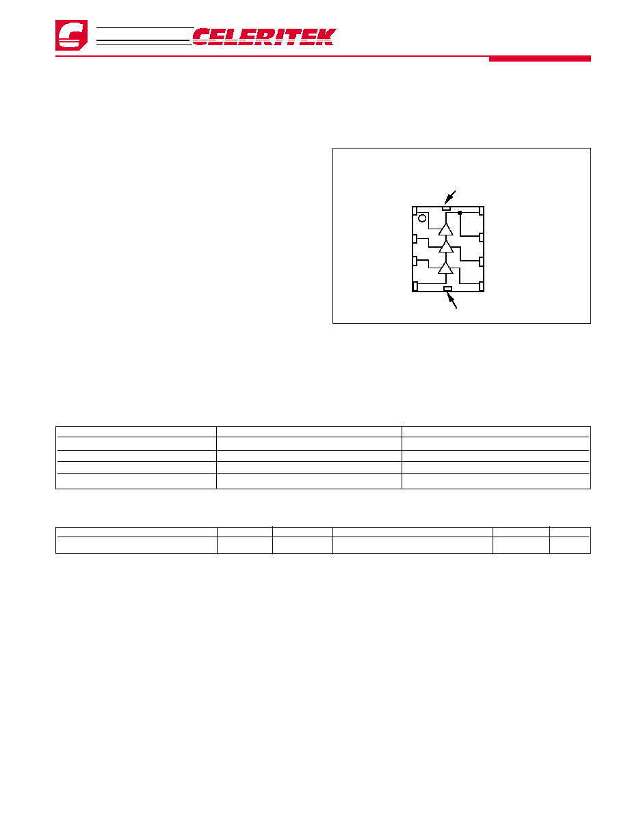
Ground Tab
Vg3 1
RF IN 4
Vg2 2
Vg1 3
7 RF OUT/+Vd3
8 RF OUT/+Vd3
5 Vd1
6 Vd2
Ground Tab
Functional Block Diagram
Absolute Maximum Ratings
Parameter
Rating
Parameter
Rating
Parameter
Rating
Drain Voltage (+Vd)
+8 V*
Power Dissipation
5 W
Operating Temperature
-30∞C to +90∞C
Drain Current (Id)
1.0 A
Thermal Resistance
20∞C/W
Channel Temperature
150∞C
RF Input Power
0 dBm*
Storage Temperature
-65∞C to +150∞C
Soldering Temperature
240∞C for 5 Sec.
DC Gate Voltage (-Vg)
-4.0 V*
BVGD
18 V
Recommended Operating Conditions
Parameter
Typ
Units
Parameter
Typ
Units
Drain Voltage (+Vd)
7.0
Volts
Operating Temperature (PC Board)
-40 to +70
∞C
* Max (+Vd) and (-Vg) under linear operation. Max potential difference across the device at 1dB gain compression point (2Vd + |-Vg|) not to exceed the minimum breakdown voltage (BVGD) of +18V.
Application Information
The CMM3566-LC is a three stage amplifier that requires a
positive and a negative supply voltages for proper operation. It is
essential when turning on the device that the negative supply be
applied before the positive supply. When turning the device off,
the positive supply should be removed before the negative supply
is removed.
The CMM3566-LC can be operated over a range of supply
voltages and bias currents. It is important that the maximum power
dissipation specification for the package be observed at all times
and that the maximum voltage across the device not be exceeded.
Circuit Design Considerations
Biasing Three negative voltages are needed to set the bias current
of the 3-stage GaAs FET power amplifier. The first stage bias is
controlled via Vg1. The second stage bias is controlled via Vg2.
The output stage is controlled via Vg3. The recommended divider
networks for each gate bias shown in the schematic. The positive
supply voltage is applied to pins 5, 6, 7 and 8. The negative volt-
age supplies control the quiescent current of the device. The quies-
cent current needs to be set at the level specified in order to get the
guaranteed RF performances.
Negative bias voltages can also be used to control the gain,
the output power and the operating current during operation of the
device.
Matching Circuits Output matching circuit is required to achieve
the output power and gain guaranteed. Celeritek's recommenda-
tion for the topology of the matching circuit is shown in the
schematic diagram of the test circuit in this data sheet.
In providing both the negative and positive bias voltages, it is
important to provide adequate de-coupling between the RF signal
and the DC voltages. Inadequate de-coupling could result in low
output power, low gain or oscillation. Celeritek recommends the
bias circuits shown in the evaluation circuit .
≠ Continued on Page 2 ≠

3236 Scott Boulevard, Santa Clara, California 95054
Phone: (408) 986-5060
Fax: (408) 986-5095
CMM3566-LC
Preliminary Product Information - November
Parameter
Condition
Min
Typ
Max
Units
Frequency Range
3.45
3.5
GHz
Gain
@ Digital power output
26
28.5
31
dB
Gain Variation
Over supply voltage
2
dB/V
Over temperature
0.03
dB/∞C
Harmonics*
2nd (Pout = +22 to +26 dBm)
-35
-30
dBc
3rd (Pout = +22 to +26 dBm) and above
-40
-35
dBc
Linear Output Power
±2.7 MHz from carrier
-43
-40
dBc/30 KHz
(Pout = +22 dBm, Data Rate = 4.096Mc/Sec
±5.25 MHz from carrier
-50
-48
dBc/30 KHz
(Pout = +22 dBm, Data Rate = 4.096Mc/Sec
Linear Output Power
±2.7 MHz from carrier
-38
-35
dBc/30 KHz
(Pout = +24 dBm, Data Rate = 4.096Mc/Sec
±5.25 MHz from carrier
-47
-45
dBc/30 KHz
(Pout = +24 dBm, Data Rate = 4.096Mc/Sec
Wideband Noise
10 MHz Bandwidth
-68
dBc
Noise Figure
Vdd = 7.0 V
5
dB
Return Loss Input
-10
-14
dB
Return Loss Output
-10
-14
dB
Positive Supply Current (Id)
Pout = +24 dBm
540
mA
Quiescent Current (Iq)
No RF
520
mA
Negative Supply Current (-Ig)
Includes external resistor divider
2.0
4.0
mA
Negative Supply Voltage (-Vg)
Into external resistor divider
-0.3
-1.5
-3.0
V
Electrical Characteristics
Unless otherwise specified, the following specifications are guaranteed at 3.45 GHz, room temperature with drain voltage (+Vd) = 7.0 V in Celeritek test fixture.
Modulation When biased as specified, the CMM3566-LC will
achieve the required adjacent channel response for the W-CDMA
linearity. Celeritek tests each product under digital modulation to
ensure compliance to system specifications.
Thermal
1. The copper pad on the backside of the CMM3566-LC must be
soldered to the ground plane.
≠ Continued from Page 1 ≠
Frequency
S11
S21
S12
S22
(GHz)
Mag
ANG
Mag
ANG
Mag
ANG
Mag
ANG
0.6
0.646
136.623
2.393
20.992
0.002
-19.228
0.804
-23.817
0.8
0.659
54.979
1.283
17.015
0.003
-80.195
0.682
-89.402
1.0
0.732
-19.826
5.119
-67.405
0.004
-158.535
0.420
-138.407
1.2
0.778
-82.663
8.080
-171.314
0.005
132.866
0.382
-152.437
1.4
0.781
-140.684
10.458
93.318
0.005
67.738
0.533
150.599
1.6
0.751
155.653
12.110
-2.432
0.007
0.028
0.650
69.917
1.8
0.770
14.916
11.272
-176.757
0.006
-124.480
0.874
-61.986
2.0
0.770
11.996
11.158
-179.876
0.006
-126.766
0.880
-63.734
2.2
0.781
-40.876
11.715
106.441
0.007
173.071
0.911
-116.517
2.4
0.772
-81.765
15.438
32.091
0.008
128.121
0.877
-177.609
2.6
0.757
-121.242
21.302
-51.262
0.010
68.938
0.771
103.364
2.8
0.640
176.329
27.182
-150.627
0.011
-13.377
0.756
13.731
3.0
0.447
86.466
29.193
105.943
0.010
-79.627
0.690
-53.854
3.2
0.516
0.714
28.413
4.707
0.011
-137.593
0.471
-91.983
3.4
0.518
-69.213
25.542
-94.768
0.010
152.682
0.383
-99.415
3.6
0.131
-149.583
24.348
164.543
0.012
93.523
0.268
-121.022
3.8
0.423
-13.907
19.130
58.878
0.011
18.708
0.257
-98.953
4.0
0.578
-59.337
14.619
-37.638
0.008
-52.138
0.278
-134.978
S-Parameters
Vdd = 7V, ID 1 & 2 = 200, ID 3 = 300
* The integrity of the input signal at an offset of 5.25 MHz has an adjacent channel performance of not greater than -52 dBc.

3236 Scott Boulevard
Santa Clara, California 95054
Phone: (408) 986-5060
Fax: (408) 986-5095
CMM3566-LC
Preliminary Product Information - November 2000
(3 of 4)
Typical Performance
Gain and Return Loss vs Frequency
Linear Output Power vs Frequency
Id & Adjacent Channel Power vs Output Power
(2.7 MHz from Carrier)
Id & Adjacent Channel Power vs Output Power
(5.25 MHz from Carrier)

3236 Scott Boulevard, Santa Clara, California 95054
Phone: (408) 986-5060
Fax: (408) 986-5095
Celeritek reserves the right to make changes without further notice to any products herein. Celeritek makes no warranty, representation or guarantee regarding the
suitability of its products for any particular purpose, nor does Celeritek assume any liability arising out of the application or use of any product or circuit, and specifically
disclaims any and all liability, including without limitation consequential or incidental damages. "Typical" parameters can and do vary in different applications. All operating
parameters, including "Typicals" must be validated for each customer application by customer's technical experts. Celeritek does not convey any license under its patent
rights nor the rights of others. Celeritek products are not designed, intended, or authorized for use as components in systems intended for surgical implant into the body,
or other applications intended to support or sustain life, or for any other application in which the failure of the Celeritek product could create a situation where personal
injury or death may occur. Should Buyer purchase or use Celeritek products for any such unintended or unauthorized application, Buyer shall indemnify and hold Celeritek
and its officers, employees, subsidiaries, affiliates, and distributors harmless against all claims, costs, damages, and expenses, and reasonable attorney fees arising out
of, directly or indirectly, any claim of personal injury or death associated with such unintended or unauthorized use, even if such claim alleges that Celeritek was negligent
regarding the design or manufacture of the part. Celeritek is a registered trademark of Celeritek, Inc. Celeritek, Inc. is an Equal Opportunity/Affirmative Action Employer.
CMM3566-LC
Preliminary Product Information - November 2000
(4 of 4)
Ordering Information
The CMM3566-LC is available in a surface mount plastic LCC-8 package and devices are available in tube or tape and reel.
Part Number for Ordering
Package
CMM3566-LC
LCC-8 surface mount power package
CMM3566-LC-000T
LCC-8 surface mount power package in tape and reel
PB-CMM3566-LC
Evaluation Board with SMA connectors for CMM3566-LC
Physical Dimensions
Vg
Vdd
R5
49.9 K
C14
100 µF
C8
0.01 µF
C4
56 pF
RF IN
(50
)
1
2
3
4
8
7
6
5
CMM3566-LC
RF OUT
(50
)
C3
0.01
µF
C6
100 pF
C7
100 pF
C9
.01 µF
C5
0.1 µF
L1 27 nH
L2 27 nH
T4
105
90∞
T3
61
155∞
C17
0.9 pF
C10*
100
pF
Vgg 1
C11
0.01
µF
C12*
100
pF
C1
0.01
µF
C2*
100
pF
Vgg 2
Vgg 3
R2
1.5K
R4
1.5K
R3
427
R1
80
* = Should be as close to leads as possible.
Recommended Matching Topology
Note: This schematic represents the topology of the matching circuit recommended by Celeritek.
Evaluation Board Schematic
Board substrate:
ER = 3.38
Thickness = 0.031 in.