 | –≠–ª–µ–∫—Ç—Ä–æ–Ω–Ω—ã–π –∫–æ–º–ø–æ–Ω–µ–Ω—Ç: PS9661 | –°–∫–∞—á–∞—Ç—å:  PDF PDF  ZIP ZIP |
DESCRIPTION
NEC's PS9661 and PS9661L are optically coupled isolators containing a GaAlAs LED on the input side and a CMOS
output IC on the output side.
These photocouplers are high common mode transient immunity (CMR), high-speed CMOS output type devices,
making them ideal for high-speed logic interface circuits.
The PS9661 is in a plastic DIP (Dual In-line Package) and the PS9661L is lead bending type (Gull-wing) for surface
mounting.
FEATURES
∑ High-speed response (25 Mbps)
∑ High common mode transient immunity (CM
H
, CM
L
= ±20 kV/
µ
s TYP.)
∑ High isolation voltage (BV = 3 750 Vr.m.s.)
∑ Pulse width distortion ( |t
PHL
-
t
PLH
| = 3 ns TYP.)
∑ Ordering number of tape product: PS9661L-E3, E4: 1 000 pcs/reel
APPLICATIONS
∑ Factory Automation Network
∑ Measurement equipment
∑ PDP
The information in this document is subject to change without notice. Before using this document, please confirm that
this is the latest version.
PS9661, PS9661L
NEC's HIGH NOISE REDUCTION
25 Mbps CMOS OUTPUT TYPE
8-PIN DIP OPTOCOUPLER
PRELIMINARY DATA SHEET
Date Published: August 2005

PAC K A GE DIMENSIO N S (UNIT : m m )
PS9661
9.25±0.25
6.5
±0.5
0 to 15∞
7.62
TOP VIEW
2.54
0.84±0.43
3
.
0
±
5
.
3
5
6
.
0
3
.
0
±
5
1
.
4
.
N
I
M
8
.
2
1.25±0.15
0.25 M
0.5±0.1
0.88±0.1
1. V
DD1
2. V
I
3. LED Anode
4. GND1
5. GND2
6. V
O
7. NC
8. V
DD2
1
2
4
3
6
5
8
7
D
L
E
I
H
S
TOP VIEW
PS9661L
6.5±0.5
0.9±0.25
9.60±0.4
2.54
0.25 M
1.25±0.15
3
.
0
±
5
.
3
9.25±0.25
0.88±0.1
1
.
0
1
.
0
+
5
0
.
0
≠
5
2
.
0
1
.
0
+
5
0
.
0
≠
1. V
DD1
2. V
I
3. LED Anode
4. GND1
5. GND2
6. V
O
7. NC
8. V
DD2
1
2
4
3
6
5
8
7
D
L
E
I
H
S
PS9661, PS9661L
Preliminary Data Sheet
PS9661, PS9661L
MA RKI NG EXAMPLE
PS9661
M301
No. 1 pin
Mark
M
Week Assembled
Year Assembled
(Last 1 Digit)
Rank Code
3 01
Country Assembled
Type Number
Assembly Lot
Preliminary Data Sheet

PS9661, PS9661L
ORDERING INFORMATION (Solder Contains Lead)
Part Number
Package
Packing Style
PS9661
8-pin DIP
Magazine case 50 pcs
PS9661L
PS9661L-E3
Embossed Tape 1 000 pcs/reel
PS9661L-E4
ORDERING INFORMATION (Pb-Free)
Part Number
Package
Packing Style
PS9661-A
8-pin DIP
Magazine case 50 pcs
PS9661L-A
PS9661L-E3-A
Embossed Tape 1 000 pcs/reel
PS9661L-E4-A
ABSOLUTE MAXIMUM RATINGS (T
A
= 25∞C, unless otherwise specified)
Parameter
Symbol
Ratings
Unit
Diode
Input Voltage
V
I
-
0.5 to V
DD1
+0.5
V
Detector
Supply Voltage
V
DD1
,
V
DD2
0 to 5.5
V
Output Voltage
V
O
-
0.5 to V
DD2
+0.5
V
Output Current
I
O
10
mA
Isolation Voltage
*1
BV
3 750
Vr.m.s.
Total Power Dissipation
P
T
150
mW
Operating Ambient Temperature
T
A
-
40 to +85
∞
C
Storage Temperature
T
stg
-
40 to +125
∞
C
*1 AC voltage for 1 minute at T
A
= 25∞C, RH = 60% between input and output.
RECOMMENDED OPERATING CONDITIONS (T
A
= 25∞C)
Parameter
Symbol
MIN.
TYP.
MAX.
Unit
High Level Input Voltage
V
IH
2.0
V
DD1
V
Low Level Input Voltage
V
IL
0
0.8
V
Supply Voltage
V
DD1
,
V
DD2
4.5
5.0
5.5
V
Rise Time
t
r
100
ns
Fall Time
t
f
Preliminary Data Sheet

PS9661, PS9661L
ELECTRICAL CHARACTERISTIC S (Recommended Operating Conditions Unless Otherwise
Specified. Note That V
DD1
= V
DD2
= 5 V.)
Parameter
Symbol
Conditions
MIN.
TYP.
*1
MAX.
Unit
Fig.
Diode
Low Level Supply Current I
DD1L
V
I
= 0 V
7.5
10.0
1
High Level Supply Current I
DD1H
V
I
= V
DD1
0.15
3.0
mA
2
Input Current
I
I
V
I
= 0 V or V
I
= V
DD1
-
10
10
µ
A
3, 4
Detector Output Supply Current
I
DD2H
V
I
= V
DD1
7
9
5
I
DD2L
V
I
= 0 V
5
9
mA
6
I
O
= -20
µ
A, V
I
= V
IH
4.4
5.0
7
High Level Output Voltage V
OH
I
O
= -4 mA, V
I
= V
IH
4.0
4.8
I
O
= 20
µ
A, V
I
= V
IL
0.01
0.1
V
8
Low Level Output Voltage
V
OL
I
O
= 4 mA, V
I
= V
IL
0.32
1.0
Coupled Isolation Resistance
R
I-O
V
I-O
= 1 kV
DC
, RH = 40 to 60%,
T
A
= 25 ∞C
10
11
Isolation Capacitance
C
I-O
V = 0 V, f = 1 MHz, T
A
= 25 ∞C
1.3
pF
Propagation Delay Time
(H L)
t
PHL
C
L
= 15 pF, CMOS Signal Levels
20
40
9
Propagation Delay Time
(L H)
t
PLH
23
40
Pulse Width
PW
40
Pulse Width Distortion
(PWD)
|
t
PHL-
t
PLH
|
3
8
Propagation Delay Skew
t
PSK
20
Rise Time
t
r
9
Fall Time
t
f
8
ns
Common Mode
Transient Immunity at
High Level Output
CM
H
V
I
= V
DD1
= V
DD2
= 5V,
V
O
>
0.8 V
DD1
, V
CM
= 1 kV, T
A
= 25 ∞C
10
20
10
Common Mode
Transient Immunity at
Low Level Output
CM
L
V
I
= V
DD1
= V
DD2
= 5V, V
I
=0V
V
O
<
0.8 V
DD1
, V
CM
= 1 kV
10
20
kV/
µ
s
*1 Typical values at T
A
= 25 ∞C
Preliminary Data Sheet

PS9661, PS9661L
USAGE CAUTIONS
1. This product is weak for static electricity by desig ned with high-speed integrated circuit so protect against static
electricity when handling.
2. By-pass capacitor of more than 0.1
µ
F is used between V
DD
and GND near device. Al so, ensure that the
distance between the leads of the photocouple r and capacitor is no more than 10 mm.
Preliminary Data Sheet

PS9661, PS9661L
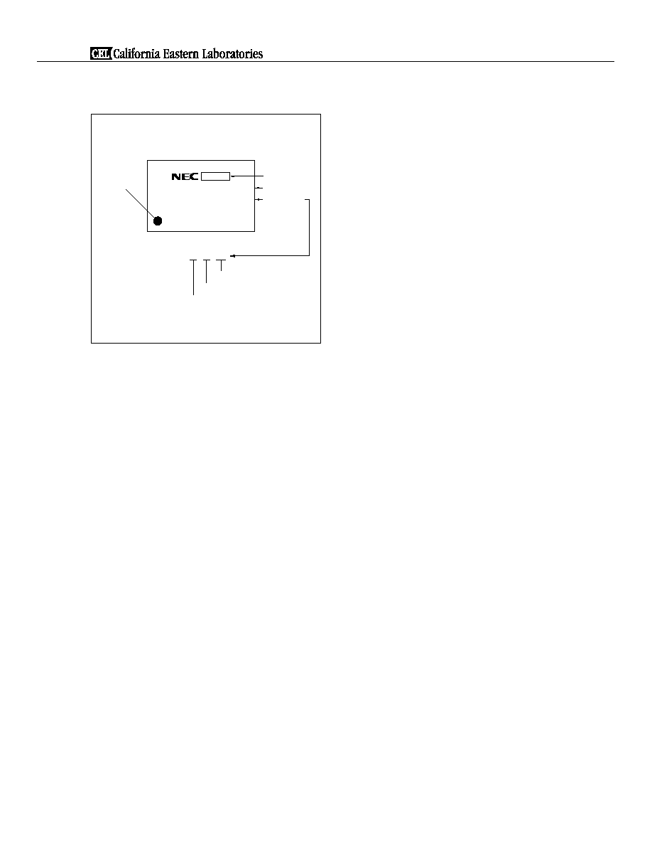
MEASUREMENT CIRCUITS FOR EL EC TR ICA L CHA RAC TER I STIC S
1
2
3
4
8
7
6
5
V
DD1
A
1
2
3
4
8
7
6
5
V
DD1
A
1
2
3
4
8
7
6
5
V
DD1
A
1
2
3
4
8
7
6
5
V
DD1
A
1
2
3
4
8
7
6
5
V
DD2
V
DD1
A
1
2
3
4
8
7
6
5
V
DD2
V
DD1
A
1
2
3
4
8
7
6
5
V
DD2
V
DD1
V
IH
V
I
O
1
2
3
4
8
7
6
5
V
DD2
V
DD1
V
IL
V
I
O
Fig. 1 I
DD1L
Fig. 2 I
DD1H
Fig. 3 I
IH
Fig. 4 I
IL
Fig. 5 I
DD2H
Fig. 6 I
DD2L
Fig. 7 V
OH
Fig. 8 V
OL
Preliminary Data Sheet

PS9661, PS9661L
F
ig . 9 t
P H L
/
t
PL H
1
2
3
4
8
7
6
5
V
DD2
V
DD1
V
I
C
L
V
O
INPUT V
I
OUTPUT V
O
50 %
t
PLH
t
PHL
0 V
5 V CMOS
V
OL
V
OH
2.5 V CMOS
90 %
10 %
90 %
10 %
PW = 40 ns
F
ig . 10 C
M H
/
C
M L
0. 1 u F
5
8
7
6
1
2
3
4
V
DD2
V
O
V
OH
V
OL
0 . 1u F 0 . 1u F
VCM
SW : B
0.8 V
0.8 V
DD
SW : A
1kV
V
CM
Life Support Applications
These NEC products are not intended for use in life support devices, appliances, or systems where the malfunction of these products can reasonably
be expected to result in personal injury. The customers of CEL using or selling these products for use in such applications do so at their own risk and
agree to fully indemnify CEL for all damages resulting from such improper use or sale.
A Business Partner of NEC Compound Semiconductor Devices, Ltd.
Preliminary Data Sheet

4590 P a t r ick Hen r y Drive
San t a C l ara, CA 9505 4- 181 7
Teleph o n e : ( 408) 919- 25 00
Facsim ile: ( 408 ) 988- 027 9
Subject: Compliance with EU Dire ctives
CEL certifies, to its kno w ledge, that semicondu ctor and laser products detailed below are compliant
with the requirements of European Union (EU) Directive 2002/95/EC Restriction on Use of Hazardous
Substances in electrical and electron ic equipment (RoHS) an d the requir e ments of EU Directive
2003/11/EC Restriction o n Penta and Octa BDE.
CEL Pb-free products ha ve the same base part n u mber with a suffix added. The suffix ≠A indicates
that the device is Pb-fre e. The ≠AZ suffix is use d to designa te devices containing Pb which are
exempted from the requirement of Ro HS directive (*). In all cases the de vices have Pb-free terminals.
All devices with these suffixes meet the require ments of the RoHS directive.
This statu s is based on CEL's understanding of t he EU Directives and kn owledge of the materials that
go into its pr oducts as of the date of disclo s ure o f this inform ation.
Re st rict e d S u bst a n c e
per RoHS
Con c e n tratio n Limit per RoHS
(value s are n o t yet fixed)
Con c e n tratio n contai ned
in CEL devices
- A
- A Z
Lead (P b)
< 100 0 PPM
Not Dete cted
(*)
Mercury
< 100 0 PPM
Not Dete cted
Cadmi u m
< 100 PPM
Not Dete cted
Hexavale nt Chromi um
< 100 0 PPM
Not Dete cted
PBB
< 1000 PPM
Not Detec t ed
PBDE
< 1000 PPM
Not Detec t ed
If you should have any additional q uestions reg a rding our d e vices and compliance t o environme n tal
standards, p l ease do not hesitate to contact your local representative.
Important Inf o rm ation and Disclaimer: Infor m ation provided b y CEL on its w ebsite or in other communi cations concertin g the subs tance
content of its pro ducts represents know ledge and b e lief as of t he date that it is provided. CEL bases its know ledge a n d belief on informa t ion
provided b y t h ird parties and make s no representa t ion or w a rran t y a s to the accurac y of such information. Efforts are u nder w a y to b e tte r
integrate informa t ion from third pa rties. CEL has ta ken and cont inue s to take reasona ble steps to provide repr esentative and ac cur a te
information but ma y not h a ve conducted destructive testing or chemical analy s is on incoming ma terials and chemicals. CEL and CE L
suppliers consid er certain inform ation to be pro p ri etar y , and thus C AS numbers and other limited information ma y not be availab le for
release.
In no event shall CEL's liability ari s ing out of such information e x cee d the total purch ase price of the CEL part ( s) at issue s old by CEL to
customer on an annual basis.
See CEL Te rms and Conditions f o r additional cl arification of w a rran t ies and liability .