 | –≠–ª–µ–∫—Ç—Ä–æ–Ω–Ω—ã–π –∫–æ–º–ø–æ–Ω–µ–Ω—Ç: PS9687L1 | –°–∫–∞—á–∞—Ç—å:  PDF PDF  ZIP ZIP |

PHOTOCOUPLER
PS9687L1,PS9687L2
-
NEPOC Series
-
HIGH CMR, 10 Mbps OPEN COLLECTOR OUTPUT TYPE
8-PIN DIP PHOTOCOUPLER
FOR
CREEPAGE
DISTANCE
OF
8
mm
DESCRIPTION
The PS9687L1 and PS9687L2 are optically coupled isolators containing a GaAlAs LED on the input side and a
photo diode and a signal processing circuit on the output side on one chip.
The PS9687L1 and PS9687L2 are designed specifically for long creepage-distance as well as high common mode
transient immunity (CMR) and high speed digital output type. Consequently, they are suitable for high speed logic
interface that needs long creepage-distance (8 mm) on mounting.
The PS9687L1 is in a plastic DIP (Dual In-line Package) and the PS9687L2 is lead bending type (Gull-wing) for
surface mounting.
FEATURES
PIN CONNECTIONS
(Top View)
1. NC
2. Anode
3. Cathode
4. NC
5. GND
6. V
O
7. NC
8. V
CC
1
2
4
3
6
5
8
7
∑ Long creepage distance (8 mm MIN.)
∑ High common mode transient immunity (CM
H
, CM
L
=
±
20 kV/
µ
s TYP.)
∑ High isolation voltage (BV = 5 000 Vr.m.s.)
∑ High-speed response (10 Mbps)
∑ Pulse width distortion (
t
PHL
-
t
PLH
= 15 ns TYP.)
∑ Open collector output
∑ Ordering number of tape product: PS9687L2-E3, E4: 1 000 pcs/reel
∑ Safety
standards
∑ UL approved: File No. E72422
∑ BSI approved: No. 8990/8991
∑ DIN EN60747-5-2 (VDE0884 Part2) approved: No.40008906 (Option)
APPLICATIONS
∑ FA
Network
∑ Measurement
equipment
∑ PDP
Document No. PN10573EJ01V0DS (1st edition)
Date Published July 2005 CP(K)
PS9687L1,PS9687L2
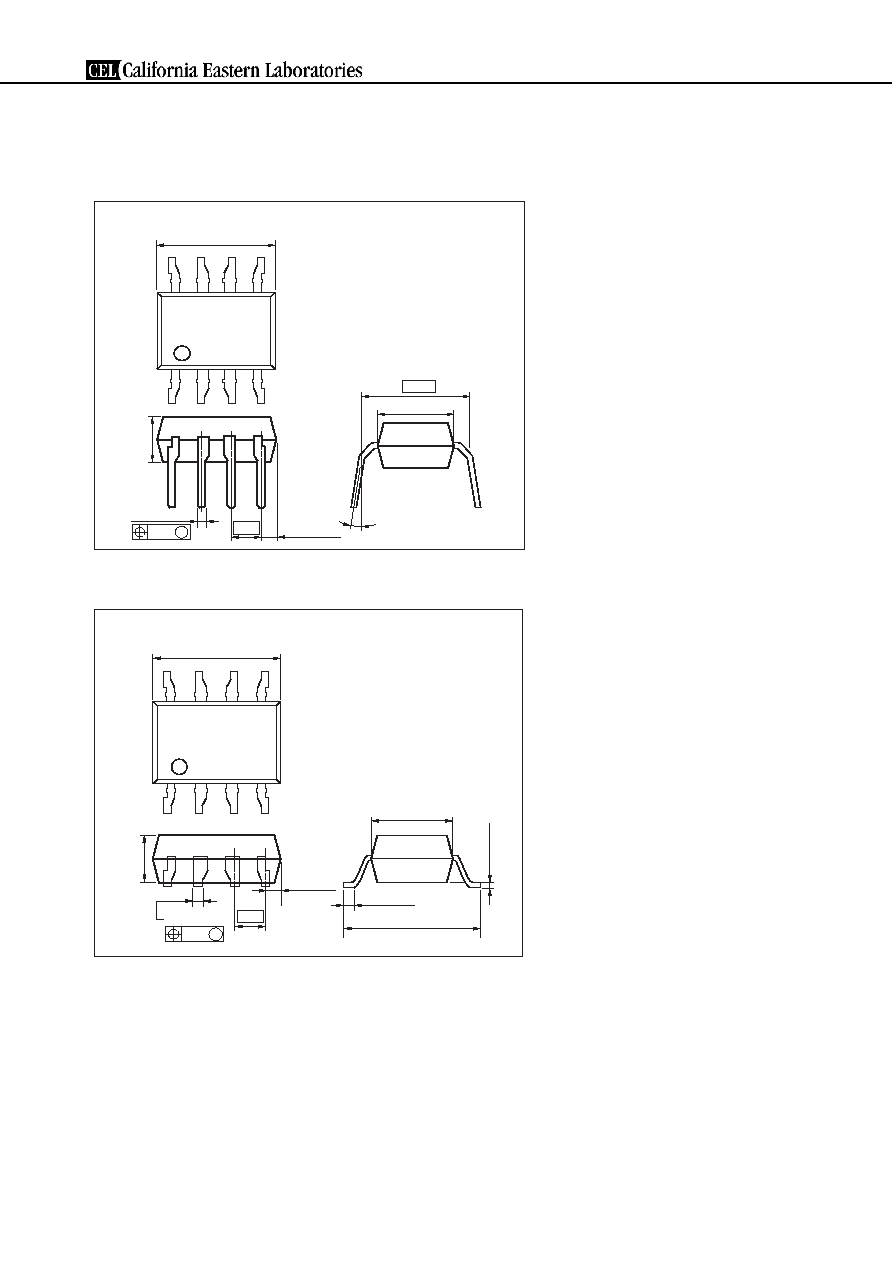
PACKAGE DIMENSIONS (UNIT: mm)
DIP Type
PS9687L1
6.5±0.5
0 to 15∞
10.16
2.54
0.84±0.43
3.5±0.3
0.25 M
0.50±0.15
1
4
8
5
9.25
+0.5
≠0.25
Lead Bending Type
PS9687L2
6.5±0.5
0.9±0.25
11.8±0.4
0.25±0.2
2.54
0.25 M
0.5±0.15
3.5±0.3
0.84±0.43
8
1
5
4
9.25
+0.5
≠0.25
Data Sheet PN10573EJ01V0DS
2
PS9687L1,PS9687L2
FUNCTIONAL DIAGRAM
8
6
5
2
3
LED
Output
ON
L
OFF
H
Shield
MARKING EXAMPLE
PS9687
NL503
Week Assembled
Year Assembled
(Last 1 Digit)
Rank Code
03
Type Number
Assembly Lot
N
JAPAN
N L
In-house Code (L: Pb-Free)
5
No. 1 pin Mark
Initial of NEC
(Engraved mark)
Data Sheet PN10573EJ01V0DS
3

PS9687L1,PS9687L2
ORDERING INFORMATION
Part Number
Order Number
Solder Plating
Specification
Packing Style
Safety Standard
Approval
Application Part
Number*
1
PS9687L1
PS9687L1-A
Pb-Free
Magazine case 50 pcs
Standard products
PS9687L1
PS9687L2
PS9687L2-A
(UL, BSI approved) PS9687L2
PS9687L2-E3
PS9687L2-E3-A
Embossed Tape 1 000 pcs/reel
PS9687L2-E4 PS9687L2-E4-A
PS9687L1-V
PS9687L1-V-A
Magazine case 50 pcs
PS9687L1
PS9687L2-V PS9687L2-V-A
PS9687L2
PS9687L2-V-E3
PS9687L2-V-E3-A
Embossed Tape 1 000 pcs/reel
PS9687L2-V-E4 PS9687L2-V-E4-A
DIN EN60747-5-2
(VDE0884 Part2)
approved (Option)
*1 For the application of the Safety Standard, following part number should be used.
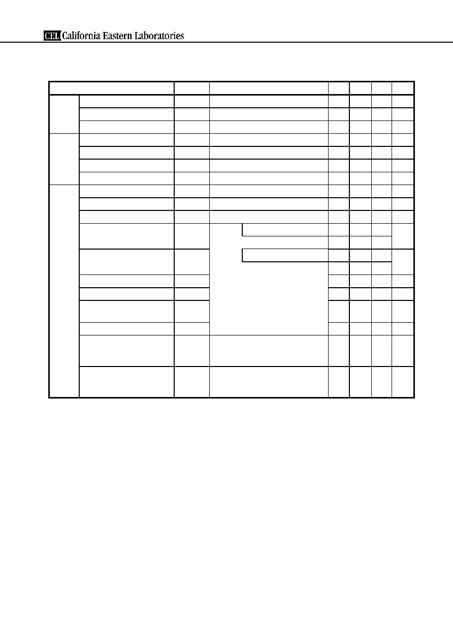
ABSOLUTE MAXIMUM RATINGS (T
A
= 25
∞
C, unless otherwise specified)
Parameter Symbol
Ratings
Unit
Diode Forward
Current
*1
I
F
30 mA
Reverse
Voltage
V
R
5 V
Detector Supply Voltage
V
CC
7 V
Output
Voltage
V
O
7 V
Output
Current
I
O
25 mA
Power
Dissipation
*2
P
C
40 mW
Isolation Voltage
*3
BV 5
000
Vr.m.s.
Operating Ambient Temperature
T
A
-
40 to +85
∞
C
Storage Temperature
T
stg
-
55 to +125
∞
C
*1 Reduced to 0.3 mA/
∞
C at T
A
= 25
∞
C or more.
*2 Applies to output pin V
O
(Collector pin). Reduced to 1.5 mW/
∞
C at T
A
= 65
∞
C or more.
*3 AC voltage for 1 minute at T
A
= 25
∞
C, RH = 60% between input and output.
Pins 1-4 shorted together, 5-8 shorted together.
RECOMMENDED OPERATING CONDITIONS (T
A
= 25
∞
C)
Parameter Symbol
MIN.
TYP.
MAX.
Unit
High Level Input Current
I
FH
6.3 10 12.0 mA
Low Level Input Voltage
V
FL
0 0.8 V
Supply Voltage
V
CC
4.5 5.0 5.5 V
TTL (R
L
= 1 k
, loads)
N
5
Pull-up Resistance
R
L
330 4
k
Data Sheet PN10573EJ01V0DS
4
PS9687L1,PS9687L2
ELECTRICAL CHARACTERISTICS (T
A
=
-
40 to +85
∞
C, unless otherwise specified)
Parameter Symbol
Conditions
MIN.
TYP.
*1
MAX.
Unit
Diode Forward
Voltage
V
F
I
F
= 10 mA, T
A
= 25
∞
C 1.4
1.65
1.8
V
Reverse
Current
I
R
V
R
= 3 V, T
A
= 25
∞
C
10
µ
A
Terminal
Capacitance
C
t
V
F
= 0 V, f = 1 MHz, T
A
= 25
∞
C
30
150
pF
Detector High Level Output Current
I
OH
V
CC
= V
O
= 5.5 V, V
F
= 0.8 V
1
100
µ
A
Low Level Output Voltage
*2
V
OL
V
CC
= 5.5 V, I
F
= 5 mA, I
OL
= 13 mA
0.35
0.6
V
High Level Supply Current
I
CCH
V
CC
= 5.5 V, I
F
= 0 mA, V
O
= Open
6
10
mA
Low Level Supply Current
I
CCL
V
CC
= 5.5 V, I
F
= 10 mA, V
O
= Open
11
13
mA
Coupled Threshold Input Current (H
L)
I
FHL
V
CC
= 5 V, V
O
= 0.8 V, R
L
= 350
2.5
5
mA
Isolation
Resistance
R
I-O
V
I-O
= 1 kV
DC
, RH = 40 to 60%, T
A
= 25
∞
C 10
11
Isolation
Capacitance
C
I-O
V = 0 V, f = 1 MHz, T
A
= 25
∞
C
0.9
5
pF
Propagation Delay Time
t
PHL
V
CC
= 5 V, T
A
= 25
∞
C
40
75
ns
(H
L)
*3
R
L
= 350
, I
F
= 7.5 mA, C
L
= 15 pF
100
Propagation Delay Time
t
PLH
T
A
= 25
∞
C
55
75
ns
(L
H)
*3
100
Rise
Time
t
r
20 ns
Fall
Time
t
f
10 ns
Pulse Width Distortion
(PWD)
*3
t
PHL-
t
PLH
15
50
ns
Propagation Delay Skew
t
PSK
60 ns
Common Mode
Transient Immunity at High Level
Output
*4
CM
H
V
CC
= 5 V, T
A
= 25
∞
C, I
F
= 0 mA,
V
O (MIN.)
= 2 V, V
CM
= 1 kV, R
L
= 350
10 20 kV/
µ
s
Common Mode
Transient Immunity at Low Level
Output
*4
CM
L
V
CC
= 5 V, T
A
= 25
∞
C, I
F
= 7.5 mA,
V
O (MAX.)
= 0.8 V, V
CM
= 1 kV, R
L
= 350
10 20 kV/
µ
s
Data Sheet PN10573EJ01V0DS
5