 | –≠–ª–µ–∫—Ç—Ä–æ–Ω–Ω—ã–π –∫–æ–º–ø–æ–Ω–µ–Ω—Ç: XR1007 | –°–∫–∞—á–∞—Ç—å:  PDF PDF  ZIP ZIP |

January 2006 - Rev 25-Jan-06
Mimix Broadband, Inc., 10795 Rockley Rd., Houston, Texas 77099
Tel: 281.988.4600 Fax: 281.988.4615 mimixbroadband.com
Characteristic Data and Specifications are subject to change without notice.
©2006 Mimix Broadband, Inc.
Export of this item may require appropriate export licensing from the U.S. Government. In purchasing these parts, U.S. Domestic customers accept
their obligation to be compliant with U.S. Export Laws.
Mimix Broadband
's 11.0-17.0 GHz GaAs MMIC receiver has a noise
figure of 2.2 dB and 20.0 dB image rejection across the band. This
device is a three stage LNA followed by an image reject resistive
pHEMT mixer and includes an integrated LO buffer amplifer. The image
reject mixer eliminates the need for a bandpass filter after the LNA to
remove thermal noise at the image frequency. I and Q mixer outputs
are provided and an external 90 degree hybrid is required to select the
desired sideband. This MMIC uses Mimix Broadband
's 0.15 µm GaAs
PHEMT device model technology, and is based upon electron beam
lithography to ensure high repeatability and uniformity. The chip has
surface passivation to protect and provide a rugged part with backside
via holes and gold metallization to allow either a conductive epoxy or
eutectic solder die attach process. This device is well suited for
Millimeter-wave Point-to-Point Radio, LMDS, SATCOM and VSAT
applications.
11.0-17.0 GHz GaAs MMIC
Receiver
Page 1 of 8
Fully Integrated Design
2.2 dB Noise Figure
13.5 dB Conversion Gain
20 dB Image Rejection
+4 dBm IIP3
+3 dBm LO drive Level
100% On-Wafer RF, DC and Noise Figure Testing
100% Visual Inspection to MIL-STD-883 Method 2010
Features
General Description
Absolute Maximum Ratings
Supply Voltage (Vd)
Supply Current (Id1), (Id3)
Gate Bias Voltage (Vg)
Input Power (RF Pin)
Storage Temperature (Tstg)
Operating Temperature (Ta)
Channel Temperature (Tch)
+6.0 VDC
250, 200 mA
+0.3 VDC
+17 dBm
-65 to +165
O
C
-55 to MTTF Table
MTTF Table
Chip Device Layout
(3) Channel temperature affects a device's MTTF. It is
recommended to keep channel temperature as low as
possible for maximum life.
3
3
Electrical Characteristics (Ambient Temperature T = 25
o
C)
Units
GHz
GHz
GHz
dB
dB
dBm
dBc
dB
dB
dBm
VDC
VDC
VDC
VDC
VDC
mA
mA
Min.
11.0
9.0
DC
-
-
-
-
-
-
-
-
-
-1.2
-1.2
-1.2
-
-
Typ.
-
-
2.0
15.0
13.5
+3.0
20.0
2.2
40.0/40.0
+4.0
+3.0
+5.0
-0.3
-0.1
-0.5
80
100
Max.
17.0
19.0
TBD
-
-
-
-
-
-
-
+6.0
+6.0
+0.1
+0.1
+0.1
200
150
Parameter
Frequency Range (RF)
Frequency Range (LO)
Frequency Range (IF)
Input Return Loss RF (S11)
Small Signal Conversion Gain RF/IF (S21)
LO Input Drive (P
LO
)
Image Rejection
Noise Figure (NF)
Isolation LO/RF
Input Third Order Intercept (IIP3)
Drain Bias Voltage (Vd1)
Drain Bias Voltage (Vd3)
Gate Bias Voltage (Vg1,2)
Gate Bias Voltage (Vg3)
Gate Bias Voltage (Vg4) Mixer, Doubler
Supply Current (Id1) (Vd1=3.0, Vg=-0.3V Typical)
Supply Current (Id3) (Vd3=5.0V,Vg=-0.1V Typical)
(1) Measured using constant current.
1
R1007
11.0-17.0 GHz GaAs MMIC
Receiver
Page 2 of 8
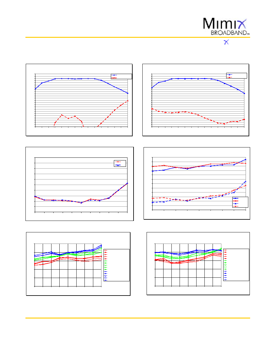
Receiver Measurements
LSB, PRF= - 20 dBm, PLO = 0, 3 & 6 dBm, VG4 = - 0.6 V, 5 RC, 08 AUG 2005:
OIP3 avg (dBm) vs. RF (GHz)
0
5
10
15
20
25
11
12
13
14
15
16
17
18
19
RF (GHz)
OIP3 avg (dBm)
OIP3, PLO (dBm)=0, RC=R10C4
OIP3, PLO (dBm)=0, RC=R10C6
OIP3, PLO (dBm)=0, RC=R11C6
OIP3, PLO (dBm)=0, RC=R12C4
OIP3, PLO (dBm)=0, RC=R13C7
OIP3, PLO (dBm)=3, RC=R10C4
OIP3, PLO (dBm)=3, RC=R10C6
OIP3, PLO (dBm)=3, RC=R11C6
OIP3, PLO (dBm)=3, RC=R12C4
OIP3, PLO (dBm)=3, RC=R13C7
OIP3, PLO (dBm)=6, RC=R10C4
OIP3, PLO (dBm)=6, RC=R10C6
OIP3, PLO (dBm)=6, RC=R11C6
OIP3, PLO (dBm)=6, RC=R12C4
OIP3, PLO (dBm)=6, RC=R13C7
USB, PRF= - 20 dBm, PLO = 0, 3 & 6 dBm, VG4 = - 0.6 V, 5 RC, 08 AUG 2005:
OIP3 avg (dBm) vs. RF (GHz)
0
5
10
15
20
25
11
12
13
14
15
16
17
18
19
RF (GHz)
OIP3 avg (dBm)
OIP3, PLO (dBm)=0, RC=R10C4
OIP3, PLO (dBm)=0, RC=R10C6
OIP3, PLO (dBm)=0, RC=R11C6
OIP3, PLO (dBm)=0, RC=R12C4
OIP3, PLO (dBm)=0, RC=R13C7
OIP3, PLO (dBm)=3, RC=R10C4
OIP3, PLO (dBm)=3, RC=R10C6
OIP3, PLO (dBm)=3, RC=R11C6
OIP3, PLO (dBm)=3, RC=R12C4
OIP3, PLO (dBm)=3, RC=R13C7
OIP3, PLO (dBm)=6, RC=R10C4
OIP3, PLO (dBm)=6, RC=R10C6
OIP3, PLO (dBm)=6, RC=R11C6
OIP3, PLO (dBm)=6, RC=R12C4
OIP3, PLO (dBm)=6, RC=R13C7
14REC0607, USB Conv. Gain (dB) and Im. Rej (dBc)
-30
-28
-26
-24
-22
-20
-18
-16
-14
-12
-10
-8
-6
-4
-2
0
2
4
6
8
10
12
14
16
18
8
9
10
11
12
13
14
15
16
17
18
19
20
21
22
RF (GHz)
CG (dB) & IR (dBc)
Conv Gain, USB
Image Rej, USB
14REC0607, LSB Conv. Gain (dB) and Im. Rej (dBc)
-30
-28
-26
-24
-22
-20
-18
-16
-14
-12
-10
-8
-6
-4
-2
0
2
4
6
8
10
12
14
16
18
8
9
10
11
12
13
14
15
16
17
18
19
20
21
22
RF (GHz)
CG (dB) & IR (dBc)
Conv Gain, LSB
Image Rej, LSB
14REC0607 Noise Figure (dB)
0.0
1.0
2.0
3.0
4.0
5.0
6.0
7.0
8.0
9.0
10.0
10
11
12
13
14
15
16
17
18
19
20
RF (GHz)
Noise Figure (dB)
USB
LSB
14REC0607 Third Order Intermod Performance, PLO = +6dBm
0
2
4
6
8
10
12
14
16
18
20
22
24
11
12
13
14
15
16
17
18
19
RF (GHz)
OIP3 & IIP3 (dBm)
IIP3, LSB
IIP3, USB
OIP3, LSB
OIP3, USB
January 2006 - Rev 25-Jan-06
Mimix Broadband, Inc., 10795 Rockley Rd., Houston, Texas 77099
Tel: 281.988.4600 Fax: 281.988.4615 mimixbroadband.com
Characteristic Data and Specifications are subject to change without notice.
©2006 Mimix Broadband, Inc.
Export of this item may require appropriate export licensing from the U.S. Government. In purchasing these parts, U.S. Domestic customers accept
their obligation to be compliant with U.S. Export Laws.
R1007

11.0-17.0 GHz GaAs MMIC
Receiver
Page 3 of 8
Receiver Measurements (cont.)
LSB, PRF= - 20 dBm, PLO = 0, 3 & 6 dBm, VG4 = - 0.6 V, 5 RC, 08 AUG 2005:
IIP3 avg (dBm) vs. RF (GHz)
-2
-1
0
1
2
3
4
5
6
7
8
9
10
11
12
13
14
11
12
13
14
15
16
17
18
19
RF (GHz)
IIP3 avg (dBm)
IIP3, PLO (dBm)=0, RC=R10C4
IIP3, PLO (dBm)=0, RC=R10C6
IIP3, PLO (dBm)=0, RC=R11C6
IIP3, PLO (dBm)=0, RC=R12C4
IIP3, PLO (dBm)=0, RC=R13C7
IIP3, PLO (dBm)=3, RC=R10C4
IIP3, PLO (dBm)=3, RC=R10C6
IIP3, PLO (dBm)=3, RC=R11C6
IIP3, PLO (dBm)=3, RC=R12C4
IIP3, PLO (dBm)=3, RC=R13C7
IIP3, PLO (dBm)=6, RC=R10C4
IIP3, PLO (dBm)=6, RC=R10C6
IIP3, PLO (dBm)=6, RC=R11C6
IIP3, PLO (dBm)=6, RC=R12C4
IIP3, PLO (dBm)=6, RC=R13C7
USB, PRF= - 20 dBm, PLO = 0, 3 & 6 dBm, VG4 = - 0.6 V, 5 RC, 08 AUG 2005:
IIP3 avg (dBm) vs. RF (GHz)
-2
-1
0
1
2
3
4
5
6
7
8
9
10
11
12
13
14
11
12
13
14
15
16
17
18
19
RF (GHz)
IIP3 avg (dBm)
IIP3, PLO (dBm)=0, RC=R10C4
IIP3, PLO (dBm)=0, RC=R10C6
IIP3, PLO (dBm)=0, RC=R11C6
IIP3, PLO (dBm)=0, RC=R12C4
IIP3, PLO (dBm)=0, RC=R13C7
IIP3, PLO (dBm)=3, RC=R10C4
IIP3, PLO (dBm)=3, RC=R10C6
IIP3, PLO (dBm)=3, RC=R11C6
IIP3, PLO (dBm)=3, RC=R12C4
IIP3, PLO (dBm)=3, RC=R13C7
IIP3, PLO (dBm)=6, RC=R10C4
IIP3, PLO (dBm)=6, RC=R10C6
IIP3, PLO (dBm)=6, RC=R11C6
IIP3, PLO (dBm)=6, RC=R12C4
IIP3, PLO (dBm)=6, RC=R13C7
January 2006 - Rev 25-Jan-06
Mimix Broadband, Inc., 10795 Rockley Rd., Houston, Texas 77099
Tel: 281.988.4600 Fax: 281.988.4615 mimixbroadband.com
Characteristic Data and Specifications are subject to change without notice.
©2006 Mimix Broadband, Inc.
Export of this item may require appropriate export licensing from the U.S. Government. In purchasing these parts, U.S. Domestic customers accept
their obligation to be compliant with U.S. Export Laws.
R1007

11.0-17.0 GHz GaAs MMIC
Receiver
Page 4 of 8
Mechanical Drawing
Bias Arrangement
Bypass Capacitors
- See App Note [2]
(Note: Engineering designator is 14REC0607)
Units: millimeters (inches) Bond pad dimensions are shown to center of bond pad.
Thickness: 0.110 +/- 0.010 (0.0043 +/- 0.0004), Backside is ground, Bond Pad/Backside Metallization: Gold
All DC/IF Bond Pads are 0.100 x 0.100 (0.004 x 0.004). All RF Bond Pads are 0.100 x 0.200 (0.004 x 0.008)
Bond pad centers are approximately 0.109 (0.004) from the edge of the chip.
Dicing tolerance: +/- 0.005 (+/- 0.0002). Approximate weight: 3.97 mg.
Bond Pad #1 (RF)
Bond Pad #2 (Vd1)
Bond Pad #9 (Vg2)
Bond Pad #10 (Vg1)
Bond Pad #3 (IF1)
Bond Pad #4 (Vd3)
Bond Pad #5 (LO)
Bond Pad #6 (Vg3)
Bond Pad #7 (Vg4)
Bond Pad #8 (IF2)
January 2006 - Rev 25-Jan-06
Mimix Broadband, Inc., 10795 Rockley Rd., Houston, Texas 77099
Tel: 281.988.4600 Fax: 281.988.4615 mimixbroadband.com
Characteristic Data and Specifications are subject to change without notice.
©2006 Mimix Broadband, Inc.
Export of this item may require appropriate export licensing from the U.S. Government. In purchasing these parts, U.S. Domestic customers accept
their obligation to be compliant with U.S. Export Laws.
R1007
1
2
3
4
5
7
8
9
1.615
(0.064)
2.000
(0.079)
0.881
(0.035)
1.681
(0.066)
2.081
(0.082)
2.081
(0.082)
6
2.281
(0.090)
2.700
(0.106)
0.881
(0.035)
1.625
(0.064)
1.681
(0.066)
0.481
(0.019)
0.0
0.0
10
1
2
3
4
5
7
8
9
6
10
Vg3
Vg4
Vg1,2
IF2
LO
IF1
RF
Vd3
Vd1
11.0-17.0 GHz GaAs MMIC
Receiver
Page 5 of 8
January 2006 - Rev 25-Jan-06
Mimix Broadband, Inc., 10795 Rockley Rd., Houston, Texas 77099
Tel: 281.988.4600 Fax: 281.988.4615 mimixbroadband.com
Characteristic Data and Specifications are subject to change without notice.
©2006 Mimix Broadband, Inc.
Export of this item may require appropriate export licensing from the U.S. Government. In purchasing these parts, U.S. Domestic customers accept
their obligation to be compliant with U.S. Export Laws.
R1007
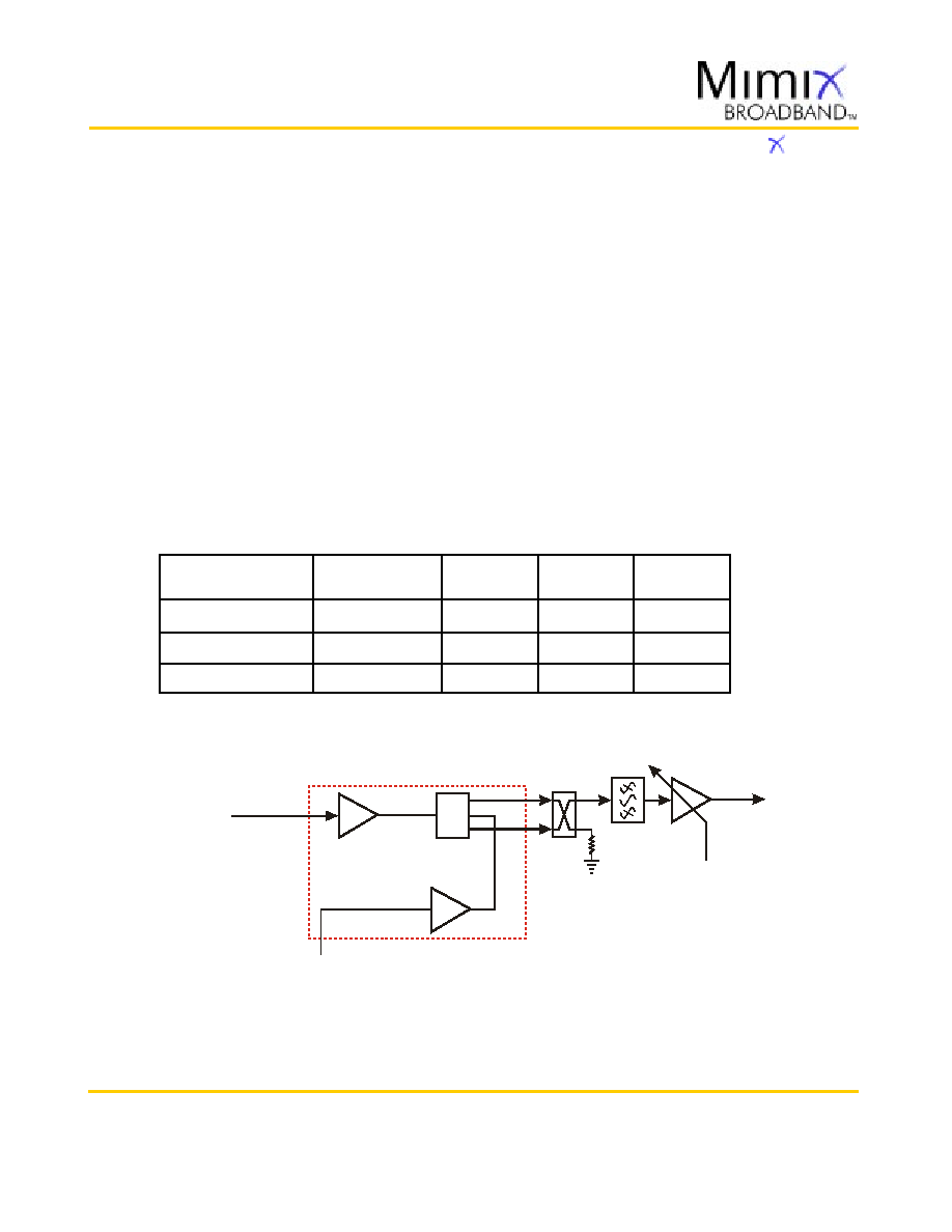
App Note [1] Biasing - As shown in the bonding diagram, this device is operated by separately biasing Vd1=3.0V with Id1=80mA and
Vd3=5.0V with Id3=100mA. Additionally, a mixer bias is also required with Vg4=-0.5V. Adjusting Vg4 above or below this value can adversely
affect conversion gain, image rejection and intercept point performance. It is also recommended to use active biasing to keep the currents
constant as the RF power and temperature vary; this gives the most reproducible results. Depending on the supply voltage available and the
power dissipation constraints, the bias circuit may be a single transistor or a low power operational amplifier, with a low value resistor in
series with the drain supply used to sense the current. The gate of the pHEMT is controlled to maintain correct drain current and thus drain
voltage. The typical gate voltage needed to do this is -0.3V. Typically the gate is protected with Silicon diodes to limit the applied voltage.
Also, make sure to sequence the applied voltage to ensure negative gate bias is available before applying the positive drain supply.
App Note [2] Bias Arrangement
-
For Parallel Stage Bias (Recommended for general applications) -- The same as Individual Stage Bias but all the drain or gate pad DC bypass
capacitors (~100-200 pF) can be combined. Additional DC bypass capacitance (~0.01 uF) is also recommended to all DC or combination (if
gate or drains are tied together) of DC bias pads.
For Individual Stage Bias -- Each DC pad (Vd1,3 and Vg1,2,3,4) needs to have DC bypass capacitance (~100-200 pF) as close to the device as
possible. Additional DC bypass capacitance (~0.01 uF) is also recommended.
Typical Application
Mimix Broadband's 11.0-17.0 GHz GaAs MMIC Receiver can be used in saturated radio applications and linear modulation schemes up to
128 QAM. The receiver can be used in upper and lower sideband applications from 11.0-17.0 GHz.
IR Mixer
LNA
Mimix Broadband MMIC-based 11.0-17.0 GHz Receiver Block Diagram
RF IN
11.0-17.0 GHz
XR1007
BPF
Coupler
IF Out
2 GHz
LO(+3.0dBm)
9.0-15.0 GHz (USB Operation)
13.0-19.0 GHz (LSB Operation)
AGC Control
Buffer
MTTF Table (TBD)
Backplate
Temperature
55 deg Celsius
75 deg Celsius
95 deg Celsius
Channel
Temperature
deg Celsius
deg Celsius
deg Celsius
FITs
E+
E+
E+
MTTF Hours
E+
E+
E+
Rth
C/W
C/W
C/W
Bias Conditions: Vd1=3.0V, Id1=80mA, Vd3=5.0V, Id3=100 mA
These numbers were calculated based on accelerated life test information and thermal model analysis received from the fabricating foundry.