 | –≠–Ľ–Ķ–ļ—ā—Ä–ĺ–Ĺ–Ĺ—č–Ļ –ļ–ĺ–ľ–Ņ–ĺ–Ĺ–Ķ–Ĺ—ā: Bt8970 | –°–ļ–į—á–į—ā—Ć:  PDF PDF  ZIP ZIP |
Document Outline
- Table of Contents
- List of Figures
- List of Tables
- 1.0 System Overview
- 2.0 Functional Description
- 3.0 Register Summary
- 4.0 Register
- 0x00ĄGlobal Modes and Status Register (global_modes)
- 0x01ĄSerial Monitor Source Select Register (serial_monitor_source)
- 0x02ĄInterrupt Mask Register Low (mask_low_reg)
- 0x03ĄInterrupt Mask Register High (mask_high_reg)
- 0x04ĄTimer Source Register (timer_source)
- 0x05ĄIRQ Source Register (irq_source)
- 0x06ĄChannel Unit Interface Modes Register (cu_interface_modes)
- 0x07ĄReceive Phase Select Register (receive_phase_select)
- 0x08ĄLinear Echo Canceller Modes Register (linear_ec_modes)
- 0x09ĄNonlinear Echo Canceller Modes Register (nonlinear_ec_modes)
- 0x0AĄDecision Feedback Equalizer Modes Register (dfe_modes)
- 0x0BĄTransmitter Modes Register (transmitter_modes)
- 0x0CĄTimer Restart Register (timer_restart)
- 0x0DĄTimer Enable Register (timer_enable)
- 0x0EĄTimer Continuous Mode Register (timer_continuous)
- 0x0FĄTest Register (reserved2)
- 0x10, 0x11ĄStartup Timer 1 Interval Register (sut1_low, sut1_high)
- 0x12, 0x13ĄStartup Timer 2 Interval Register (sut2_low, sut2_high)
- 0x14, 0x15ĄStartup Timer 3 Interval Register (sut3_low, sut3_high)
- 0x16, 0x17ĄStartup Timer 4 Interval Register (sut4_low, sut4_high)
- 0x18, 0x19ĄMeter Timer Interval Register (meter_low, meter_high)
- 0x1A, 0x1BĄSNR Alarm Timer Interval Register (snr_timer_low, snr_timer_high)
- 0x1C, 0x1DĄGeneral Purpose Timer 3 Interval Register (t3_low, t3_high)
- 0x1E, 0x1FĄGeneral Purpose Timer 4 Interval Register (t4_low, t4_high)
- 0x20ĄTest Register (reserved9)
- 0x21ĄADC Control Register (adc_control)
- 0x22ĄPLL Modes Register (pll_modes)
- 0x23ĄTest Register (reserved10)
- 0x24, 0x25ĄTiming Recovery PLL Phase Offset Register (pll_phase_offset_low, pll_phase_offset_high)
- 0x26, 0x27ĄReceiver DC Offset Register (dc_offset_low, dc_offset_high)
- 0x28ĄTransmitter Calibration Register (tx_calibrate)
- 0x29ĄTransmitter Gain Register (tx_gain)
- 0x2A, 0x2BĄNoise-Level Histogram Threshold Register (noise_histogram_th_low, noise_histogram_th_h...
- 0x2C, 0x2DĄError Predictor Pause Threshold Register (ep_pause_th_low, ep_pause_th_high)
- 0x2EĄScrambler Synchronization Threshold Register (scr_sync_th)
- 0x30, 0x31ĄFar-End High Alarm Threshold Register (far_end_high_alarm_th_low, far_end_high_alarm_t...
- 0x32, 0x33ĄFar-End Low Alarm Threshold Register (far_end_low_alarm_th_low, far_end_low_alarm_th_h...
- 0x34, 0x35ĄSNR Alarm Threshold Register (snr_alarm_th_low, snr_alarm_th_high)
- 0x36, 0x37ĄCursor Level Register (cursor_level_low, cursor_level_high)
- 0x38, 0x39ĄDAGC Target Register (dagc_target_low, dagc_target_high)
- 0x3AĄSymbol Detector Modes Register (detector_modes)
- 0x3BĄPeak Detector Delay Register (peak_detector_delay)
- 0x3CĄDigital AGC Modes Register (dagc_modes)
- 0x3DĄFeed Forward Equalizer Modes Register (ffe_modes)
- 0x3EĄError Predictor Modes Register (ep_modes)
- 0x40, 0x41ĄPhase Detector Meter Register (pdm_low, pdm_high)
- 0x42ĄOverflow Meter Register (overflow_meter)
- 0x44, 0x45ĄDC Level Meter Register (dc_meter_low, dc_meter_high)
- 0x46, 0x47ĄSignal Level Meter Register (slm_low, slm_high)
- 0x48, 0x49ĄFar-End Level Meter Register (felm_low, felm_high)
- 0x4A, 0x4BĄNoise Level Histogram Meter Register (noise_histogram_low, noise_histogram_high)
- 0x4C, 0x4DĄBit Error Rate Meter Register (ber_meter_low, ber_meter_high)
- 0x4EĄSymbol Histogram Meter Register (symbol_histogram)
- 0x50, 0x51ĄNoise Level Meter Register (nlm_low, nlm_high)
- 0x5E, 0x5FĄPLL Frequency Register (pll_frequency_low, pll_frequency_high)
- 0x70ĄLEC Read Tap Select Register (linear_ec_tap_select_read)
- 0x71ĄLEC Write Tap Select Register (linear_ec_tap_select_write)
- 0x72ĄNEC Read Tap Select Register (nonlinear_ec_tap_select_read)
- 0x73ĄNEC Write Tap Select Register (nonlinear_ec_tap_select_write)
- 0x74ĄDFE Read Tap Select Register (dfe_tap_select_read)
- 0x75ĄDFE Write Tap Select Register (dfe_tap_select_write)
- 0x76ĄScratch Pad Read Tap Select (sp_tap_select_read)
- 0x77ĄScratch Pad Write Tap Select (sp_tap_select_write)
- 0x78ĄEqualizer Read Select Register (eq_add_read)
- 0x79ĄEqualizer Write Select Register (eq_add_write)
- 0x7AĄEqualizer Microcode Read Select Register (eq_microcode_add_read)
- 0x7BĄEqualizer Microcode Write Select Register (eq_microcode_add_write)
- 0x7CÖ0x7FĄAccess Data Register (access_data_byte3:0)
- 5.0 Electrical & Mechanical Specifications
- Sales Offices

P
rel
im
in
ary
R
evi
ew
Data Sheet
Conexant
100101B
Preliminary Information/Conexant Proprietary and Confidential
November 2000
Advance Information
This document contains information on a product under development. The parametric information
contains target parameters that are subject to change.
1
1
/29/00
10:00 A.M.
Bt8970
Single-Chip HDSL Transceiver
Functional Block Diagram
The Bt8970 is a full-duplex 2B1Q transceiver based on Rockwell's High-Bit-Rate Digital
Subscriber Line (HDSL) technology. It supports transmission of more than 18,000 feet
over 26 AWG copper telephone wire without repeaters. Small size and low power dissipa-
tion makes the Bt8970 ideal for line-powered digital access, voice pairgain, and HDSL sys-
tems.
The Bt8970 is a highly integrated device that includes all of the active circuitry needed
for a complete 2B1Q transceiver. In the receive portion of the Bt8970, a variable gain
amplifier optimizes the signal level according to the dynamic range of the analog-to-digital
converter. Once the signal is digitized, sophisticated adaptive echo cancellation, equaliza-
tion, and detection DSP algorithms reproduce the originally transmitted far-end signal.
In the transmitter, the transmit source and scrambler operation is programmable via
the microcomputer interface. A highly linear digital-to-analog converter with programma-
ble gain sets the transmission power for optimal performance. A pulse-shaping filter and a
low-distortion line driver generate the signal characteristics needed to drive a large range
of subscriber lines at low-bit error rates.
Startup and performance monitoring operations are controlled via the microprocessor
interface. C-language source code supporting these operations is supplied under a no-fee
license agreement from Rockwell. The Bt8970 includes a glueless interface to both Intel
and Motorola microprocessors.
Distinguishing Features
∑
Single-chip 2B1Q transceiver solu-
tion
∑
All 2B1Q transceiver functions inte-
grated into a single monolithic device
≠ Receiver gain control and A/D
converter
≠ DSP functions including echo
cancellation, equalization, timing
recovery, and symbol detection
≠ Programmable gain transmit
DAC, pulse-shaping filter, and line
driver
∑
Supports operation from 160 to
1552 kbps
∑
Capable of transceiving over the
ANSI T1E1.4/94-006 and ETSI ETR
152 HDSL test loops
∑
Flexible Monitoring and Control
≠ Glueless interface to Intel 8051
and Motorola 68302 processors
≠ Access to embedded filters, per-
formance meters and timers
∑
Backwards compatible with Bt8952
and Bt8960 software API commands
∑
Pin compatible with Bt8960
∑
JTAG/IEEE Std 1149.1-1990
compliant
∑
Single +5 V power supply operation
with option for 3.3 V to reduce power
consumption
∑
100-pin PQFP package
∑
≠40įC to +85įC operation
∑
700 mW power consumption at 784
kbps (max using 3.3 V option)
Applications
∑
E1 and T1 HDSL transport
∑
Voice/data pairgain systems
∑
Internet connectivity
∑
ISDN basic-rate interface
concentrators
∑
Extended range fractional T1/E1
∑
Cellular/microcellular base stations
∑
Personal Communications Systems
(PCS) radio ports and cell switches

P
rel
im
inary
R
ev
iew
© 1997, 2000,
Conexant Systems, Inc.
All Rights Reserved.
Information in this document is provided in connection with Conexant Systems, Inc. ("Conexant") products. These materials are
provided by Conexant as a service to its customers and may be used for informational purposes only. Conexant assumes no
responsibility for errors or omissions in these materials. Conexant may make changes to specifications and product descriptions at
any time, without notice. Conexant makes no commitment to update the information and shall have no responsibility whatsoever for
conflicts or incompatibilities arising from future changes to its specifications and product descriptions.
No license, express or implied, by estoppel or otherwise, to any intellectual property rights is granted by this document. Except as
provided in Conexant's Terms and Conditions of Sale for such products, Conexant assumes no liability whatsoever.
THESE MATERIALS ARE PROVIDED "AS IS" WITHOUT WARRANTY OF ANY KIND, EITHER EXPRESS OR IMPLIED, RELATING
TO SALE AND/OR USE OF CONEXANT PRODUCTS INCLUDING LIABILITY OR WARRANTIES RELATING TO FITNESS FOR A
PARTICULAR PURPOSE, CONSEQUENTIAL OR INCIDENTAL DAMAGES, MERCHANTABILITY, OR INFRINGEMENT OF ANY
PATENT, COPYRIGHT OR OTHER INTELLECTUAL PROPERTY RIGHT. CONEXANT FURTHER DOES NOT WARRANT THE
ACCURACY OR COMPLETENESS OF THE INFORMATION, TEXT, GRAPHICS OR OTHER ITEMS CONTAINED WITHIN THESE
MATERIALS. CONEXANT SHALL NOT BE LIABLE FOR ANY SPECIAL, INDIRECT, INCIDENTAL, OR CONSEQUENTIAL
DAMAGES, INCLUDING WITHOUT LIMITATION, LOST REVENUES OR LOST PROFITS, WHICH MAY RESULT FROM THE USE
OF THESE MATERIALS.
Conexant products are not intended for use in medical, lifesaving or life sustaining applications. Conexant customers using or selling
Conexant products for use in such applications do so at their own risk and agree to fully indemnify Conexant for any damages
resulting from such improper use or sale.
The following are trademarks of Conexant Systems, Inc.: ConexantTM, the Conexant C symbol, and "What's Next in Communications
Technologies"TM. Product names or services listed in this publication are for identification purposes only, and may be trademarks of
third parties. Third-party brands and names are the property of their respective owners.
For additional disclaimer information, please consult Conexant's Legal Information posted at
www.conexant.com
, which is
incorporated by reference.
Reader Response: Conexant strives to produce quality documentation and welcomes your feedback. Please send comments and
suggestions to
tech.pubs@conexant.com
. For technical questions, contact your local Conexant
sales office
or field applications
engineer.
100101B
Conexant
Preliminary Information/Conexant Proprietary and Confidential
1
1
/29/00
10:00 A.M.
Ordering Information
Revision History
Model Number
Package
Ambient Temperature Range
Bt8970EHF
100-Pin Plastic Quad Flat Pack
(PQFP)
≠40įC to +85įC
Revision
Level
Date
Description
A
Advance
July 1998
Created
B
--
November 2000
Conexant template

P
rel
im
in
ary
R
evi
ew
100101B
Conexant
iii
Preliminary Information/Conexant Proprietary and Confidential
1
1
/29
/
00 10:00 A.M.
Table of Contents
List of Figures
. . . . . . . . . . . . . . . . . . . . . . . . . . . . . . . . . . . . . . . . . . . . . . . . . . . . . . . . . . . . . . . . . . . . . . . . . v
List of Tables
. . . . . . . . . . . . . . . . . . . . . . . . . . . . . . . . . . . . . . . . . . . . . . . . . . . . . . . . . . . . . . . . . . . . . . . . . vii
1.0
System Overview
. . . . . . . . . . . . . . . . . . . . . . . . . . . . . . . . . . . . . . . . . . . . . . . . . . . . . . . . . . . . . . . 1-1
1.1
Functional Summary
. . . . . . . . . . . . . . . . . . . . . . . . . . . . . . . . . . . . . . . . . . . . . . . . . . . . . . . . . 1-1
1.1.1
Transmit Section
. . . . . . . . . . . . . . . . . . . . . . . . . . . . . . . . . . . . . . . . . . . . . . . . . . . . . . 1-3
1.1.2
Receive Section
. . . . . . . . . . . . . . . . . . . . . . . . . . . . . . . . . . . . . . . . . . . . . . . . . . . . . . . 1-3
1.1.3
Timing Recovery and Clock Interface
. . . . . . . . . . . . . . . . . . . . . . . . . . . . . . . . . . . . . . . 1-3
1.1.4
Microcomputer Interface
. . . . . . . . . . . . . . . . . . . . . . . . . . . . . . . . . . . . . . . . . . . . . . . . 1-4
1.1.5
Test and Diagnostic Interface (JTAG)
. . . . . . . . . . . . . . . . . . . . . . . . . . . . . . . . . . . . . . . . 1-4
1.2
Pin Descriptions
. . . . . . . . . . . . . . . . . . . . . . . . . . . . . . . . . . . . . . . . . . . . . . . . . . . . . . . . . . . . 1-5
2.0
Functional Description
. . . . . . . . . . . . . . . . . . . . . . . . . . . . . . . . . . . . . . . . . . . . . . . . . . . . . . . . . . 2-1
2.1
Transmit Section
. . . . . . . . . . . . . . . . . . . . . . . . . . . . . . . . . . . . . . . . . . . . . . . . . . . . . . . . . . . . 2-1
2.1.1
Symbol Source Selector/Scrambler
. . . . . . . . . . . . . . . . . . . . . . . . . . . . . . . . . . . . . . . . . 2-1
2.1.2
Variable Gain Digital-to-Analog Converter
. . . . . . . . . . . . . . . . . . . . . . . . . . . . . . . . . . . . 2-3
2.1.3
Pulse-Shaping Filter
. . . . . . . . . . . . . . . . . . . . . . . . . . . . . . . . . . . . . . . . . . . . . . . . . . . . 2-3
2.1.4
Line Driver
. . . . . . . . . . . . . . . . . . . . . . . . . . . . . . . . . . . . . . . . . . . . . . . . . . . . . . . . . . . 2-3
2.2
Receive Section
. . . . . . . . . . . . . . . . . . . . . . . . . . . . . . . . . . . . . . . . . . . . . . . . . . . . . . . . . . . . 2-4
2.2.1
Variable Gain Amplifier
. . . . . . . . . . . . . . . . . . . . . . . . . . . . . . . . . . . . . . . . . . . . . . . . . . 2-4
2.2.2
Analog-to-Digital Converter
. . . . . . . . . . . . . . . . . . . . . . . . . . . . . . . . . . . . . . . . . . . . . . 2-4
2.2.3
Digital Signal Processor
. . . . . . . . . . . . . . . . . . . . . . . . . . . . . . . . . . . . . . . . . . . . . . . . . 2-5
2.2.4
Echo Canceller
. . . . . . . . . . . . . . . . . . . . . . . . . . . . . . . . . . . . . . . . . . . . . . . . . . . . . . . . 2-7
2.2.5
Equalizer
. . . . . . . . . . . . . . . . . . . . . . . . . . . . . . . . . . . . . . . . . . . . . . . . . . . . . . . . . . . . 2-8
2.2.6
Detector
. . . . . . . . . . . . . . . . . . . . . . . . . . . . . . . . . . . . . . . . . . . . . . . . . . . . . . . . . . . . . 2-9
2.3
Timing Recovery and Clock Interface
. . . . . . . . . . . . . . . . . . . . . . . . . . . . . . . . . . . . . . . . . . . 2-12
2.4
Channel Unit Interface
. . . . . . . . . . . . . . . . . . . . . . . . . . . . . . . . . . . . . . . . . . . . . . . . . . . . . . 2-14

P
rel
im
in
ary
R
evi
ew
Table of Contents
Bt8970
Single-Chip HDSL Transceiver
iv
Conexant
100101B
Preliminary Information/Conexant Proprietary and Confidential
1
1
/29
/
00 10:00 A.M.
2.5
Microcomputer Interface
. . . . . . . . . . . . . . . . . . . . . . . . . . . . . . . . . . . . . . . . . . . . . . . . . . . . . 2-16
2.5.1
Source Code
. . . . . . . . . . . . . . . . . . . . . . . . . . . . . . . . . . . . . . . . . . . . . . . . . . . . . . . . 2-16
2.5.2
Microcomputer Read/Write
. . . . . . . . . . . . . . . . . . . . . . . . . . . . . . . . . . . . . . . . . . . . . . 2-16
2.5.3
Interrupt Request
. . . . . . . . . . . . . . . . . . . . . . . . . . . . . . . . . . . . . . . . . . . . . . . . . . . . . 2-17
2.5.4
Reset
. . . . . . . . . . . . . . . . . . . . . . . . . . . . . . . . . . . . . . . . . . . . . . . . . . . . . . . . . . . . . . 2-17
2.5.5
Registers
. . . . . . . . . . . . . . . . . . . . . . . . . . . . . . . . . . . . . . . . . . . . . . . . . . . . . . . . . . . 2-17
2.5.6
Timers
. . . . . . . . . . . . . . . . . . . . . . . . . . . . . . . . . . . . . . . . . . . . . . . . . . . . . . . . . . . . . 2-17
2.6
Test and Diagnostic Interface (JTAG)
. . . . . . . . . . . . . . . . . . . . . . . . . . . . . . . . . . . . . . . . . . . . 2-19
3.0
Register Summary
. . . . . . . . . . . . . . . . . . . . . . . . . . . . . . . . . . . . . . . . . . . . . . . . . . . . . . . . . . . . . . 3-1
4.0
Register
. . . . . . . . . . . . . . . . . . . . . . . . . . . . . . . . . . . . . . . . . . . . . . . . . . . . . . . . . . . . . . . . . . . . . . . 4-1
5.0
Electrical & Mechanical Specifications
. . . . . . . . . . . . . . . . . . . . . . . . . . . . . . . . . . . . . . . . . . . 5-1
5.1
Absolute Maximum Ratings
. . . . . . . . . . . . . . . . . . . . . . . . . . . . . . . . . . . . . . . . . . . . . . . . . . . 5-1
5.2
Recommended Operating Conditions
. . . . . . . . . . . . . . . . . . . . . . . . . . . . . . . . . . . . . . . . . . . . 5-2
5.3
Electrical Characteristics
. . . . . . . . . . . . . . . . . . . . . . . . . . . . . . . . . . . . . . . . . . . . . . . . . . . . . 5-3
5.4
Clock Timing
. . . . . . . . . . . . . . . . . . . . . . . . . . . . . . . . . . . . . . . . . . . . . . . . . . . . . . . . . . . . . . . 5-4
5.5
Channel Unit Interface Timing
. . . . . . . . . . . . . . . . . . . . . . . . . . . . . . . . . . . . . . . . . . . . . . . . . . 5-6
5.6
Microcomputer Interface Timing
. . . . . . . . . . . . . . . . . . . . . . . . . . . . . . . . . . . . . . . . . . . . . . . 5-10
5.6.1
Test and Diagnostic Interface Timing
. . . . . . . . . . . . . . . . . . . . . . . . . . . . . . . . . . . . . . . 5-15
5.6.2
Analog Specifications
. . . . . . . . . . . . . . . . . . . . . . . . . . . . . . . . . . . . . . . . . . . . . . . . . . 5-17
5.6.3
Test Conditions
. . . . . . . . . . . . . . . . . . . . . . . . . . . . . . . . . . . . . . . . . . . . . . . . . . . . . . 5-19
5.7
Timing Measurements
. . . . . . . . . . . . . . . . . . . . . . . . . . . . . . . . . . . . . . . . . . . . . . . . . . . . . . 5-21
5.8
Mechanical Specifications
. . . . . . . . . . . . . . . . . . . . . . . . . . . . . . . . . . . . . . . . . . . . . . . . . . . 5-23

P
rel
im
in
ary
R
evi
ew
Bt8970
List of Figures
Single-Chip HDSL Transceiver
100101B
Conexant
v
Preliminary Information/Conexant Proprietary and Confidential
1
1
/29
/
00 10:00 A.M.
List of Figures
Figure 1-1.
HDSL T1/E1 Terminal . . . . . . . . . . . . . . . . . . . . . . . . . . . . . . . . . . . . . . . . . . . . . . . . . . . . . 1-1
Figure 1-2.
Bt8970 Detailed Block Diagram . . . . . . . . . . . . . . . . . . . . . . . . . . . . . . . . . . . . . . . . . . . . . . 1-2
Figure 1-3.
Pin Diagram . . . . . . . . . . . . . . . . . . . . . . . . . . . . . . . . . . . . . . . . . . . . . . . . . . . . . . . . . . . . 1-5
Figure 2-1.
Transmit Section Block Diagram . . . . . . . . . . . . . . . . . . . . . . . . . . . . . . . . . . . . . . . . . . . . . 2-1
Figure 2-2.
First-Order Echo Cancellation Using the Variable Gain Amplifier . . . . . . . . . . . . . . . . . . . . . 2-4
Figure 2-3.
Receiver Digital Signal Processing . . . . . . . . . . . . . . . . . . . . . . . . . . . . . . . . . . . . . . . . . . . 2-5
Figure 2-4.
Digital Front-End Block Diagram . . . . . . . . . . . . . . . . . . . . . . . . . . . . . . . . . . . . . . . . . . . . . 2-6
Figure 2-5.
Timing Recovery and Clock Interface Block Diagram . . . . . . . . . . . . . . . . . . . . . . . . . . . . 2-12
Figure 2-6.
Serial Sign-Bit First Mode . . . . . . . . . . . . . . . . . . . . . . . . . . . . . . . . . . . . . . . . . . . . . . . . . 2-14
Figure 2-7.
Parallel Master Mode. . . . . . . . . . . . . . . . . . . . . . . . . . . . . . . . . . . . . . . . . . . . . . . . . . . . . 2-14
Figure 2-8.
Parallel Slave Mode . . . . . . . . . . . . . . . . . . . . . . . . . . . . . . . . . . . . . . . . . . . . . . . . . . . . . . 2-15
Figure 5-1.
MCLK Timing Requirements . . . . . . . . . . . . . . . . . . . . . . . . . . . . . . . . . . . . . . . . . . . . . . . . 5-4
Figure 5-2.
Clock Control Timing . . . . . . . . . . . . . . . . . . . . . . . . . . . . . . . . . . . . . . . . . . . . . . . . . . . . . . 5-5
Figure 5-3.
Channel Unit Interface Timing, Parallel Master Mode . . . . . . . . . . . . . . . . . . . . . . . . . . . . . 5-6
Figure 5-4.
Channel Unit Interface Timing, Parallel Slave Mode . . . . . . . . . . . . . . . . . . . . . . . . . . . . . . 5-8
Figure 5-5.
Channel Unit Interface Timing, Serial Mode . . . . . . . . . . . . . . . . . . . . . . . . . . . . . . . . . . . . 5-9
Figure 5-6.
MCI Write Timing, Intel Mode (MOTEL = 0) . . . . . . . . . . . . . . . . . . . . . . . . . . . . . . . . . . . 5-12
Figure 5-7.
MCI Write Timing, Motorola Mode (MOTEL = 1). . . . . . . . . . . . . . . . . . . . . . . . . . . . . . . . 5-12
Figure 5-8.
MCI Read Timing, Intel Mode (MOTEL = 0). . . . . . . . . . . . . . . . . . . . . . . . . . . . . . . . . . . . 5-13
Figure 5-9.
MCI Read Timing, Motorola Mode (MOTEL = 1) . . . . . . . . . . . . . . . . . . . . . . . . . . . . . . . . 5-14
Figure 5-10.
Internal Write Timing. . . . . . . . . . . . . . . . . . . . . . . . . . . . . . . . . . . . . . . . . . . . . . . . . . . . . 5-15
Figure 5-11.
JTAG Interface Timing . . . . . . . . . . . . . . . . . . . . . . . . . . . . . . . . . . . . . . . . . . . . . . . . . . . . 5-16
Figure 5-12.
SMON Timing . . . . . . . . . . . . . . . . . . . . . . . . . . . . . . . . . . . . . . . . . . . . . . . . . . . . . . . . . . 5-16
Figure 5-13.
Transmitted Pulse Template. . . . . . . . . . . . . . . . . . . . . . . . . . . . . . . . . . . . . . . . . . . . . . . . 5-18
Figure 5-14.
Transmitter Test Circuit . . . . . . . . . . . . . . . . . . . . . . . . . . . . . . . . . . . . . . . . . . . . . . . . . . . 5-19
Figure 5-15.
Standard Output Load (Totem Pole and Three-State Outputs). . . . . . . . . . . . . . . . . . . . . . 5-20
Figure 5-16.
Open-Drain Output Load (IRQ) . . . . . . . . . . . . . . . . . . . . . . . . . . . . . . . . . . . . . . . . . . . . . 5-20
Figure 5-17.
Input Waveforms for Timing Tests . . . . . . . . . . . . . . . . . . . . . . . . . . . . . . . . . . . . . . . . . . 5-21
Figure 5-18.
Output Waveforms for Timing Tests . . . . . . . . . . . . . . . . . . . . . . . . . . . . . . . . . . . . . . . . . 5-21
Figure 5-19.
Output Waveforms for Three-state Enable and Disable Tests . . . . . . . . . . . . . . . . . . . . . . 5-22
Figure 5-20.
100-Pin Plastic Quad Flat Pack (PQFP) . . . . . . . . . . . . . . . . . . . . . . . . . . . . . . . . . . . . . . . 5-23

P
rel
im
in
ary
R
evi
ew
List of Figures
Bt8970
Single-Chip HDSL Transceiver
vi
Conexant
100101B
Preliminary Information/Conexant Proprietary and Confidential
1
1
/29
/
00 10:00 A.M.

P
rel
im
in
ary
R
evi
ew
Bt8970
List of Tables
Single-Chip HDSL Transceiver
100101B
Conexant
vii
Preliminary Information/Conexant Proprietary and Confidential
1
1
/29
/
00 10:00 A.M.
List of Tables
Table 1-1.
Pin Descriptions . . . . . . . . . . . . . . . . . . . . . . . . . . . . . . . . . . . . . . . . . . . . . . . . . . . . . . . . . . 1-6
Table 1-2.
Hardware Signal Definitions . . . . . . . . . . . . . . . . . . . . . . . . . . . . . . . . . . . . . . . . . . . . . . . . . 1-7
Table 2-1.
Symbol Source Selector/Scrambler Modes . . . . . . . . . . . . . . . . . . . . . . . . . . . . . . . . . . . . . . 2-2
Table 2-2.
Four-Level Bit-to-Symbol Conversions . . . . . . . . . . . . . . . . . . . . . . . . . . . . . . . . . . . . . . . . . 2-2
Table 2-3.
Two-Level Bit-to-Symbol Conversions . . . . . . . . . . . . . . . . . . . . . . . . . . . . . . . . . . . . . . . . . 2-2
Table 2-4.
Two-Level Symbol-to-Bit Conversion . . . . . . . . . . . . . . . . . . . . . . . . . . . . . . . . . . . . . . . . . . 2-9
Table 2-5.
Four-Level Symbol-to-Bit Conversion . . . . . . . . . . . . . . . . . . . . . . . . . . . . . . . . . . . . . . . . . 2-10
Table 2-6.
Crystal Oscillator Circuit Component Values . . . . . . . . . . . . . . . . . . . . . . . . . . . . . . . . . . . . 2-13
Table 2-7.
Timers . . . . . . . . . . . . . . . . . . . . . . . . . . . . . . . . . . . . . . . . . . . . . . . . . . . . . . . . . . . . . . . . . 2-18
Table 2-8.
JTAG Device Identification Register. . . . . . . . . . . . . . . . . . . . . . . . . . . . . . . . . . . . . . . . . . . 2-19
Table 3-1.
Register Table . . . . . . . . . . . . . . . . . . . . . . . . . . . . . . . . . . . . . . . . . . . . . . . . . . . . . . . . . . . . 3-1
Table 5-1.
Absolute Maximum Ratings . . . . . . . . . . . . . . . . . . . . . . . . . . . . . . . . . . . . . . . . . . . . . . . . . 5-1
Table 5-2.
Recommended Operating Conditions . . . . . . . . . . . . . . . . . . . . . . . . . . . . . . . . . . . . . . . . . . 5-2
Table 5-3.
Electrical Characteristics . . . . . . . . . . . . . . . . . . . . . . . . . . . . . . . . . . . . . . . . . . . . . . . . . . . . 5-3
Table 5-4.
External Clock Timing Requirements (MCLK) . . . . . . . . . . . . . . . . . . . . . . . . . . . . . . . . . . . . 5-4
Table 5-5.
HCLK Switching Characteristics . . . . . . . . . . . . . . . . . . . . . . . . . . . . . . . . . . . . . . . . . . . . . . 5-4
Table 5-6.
Symbol Clock (QCLK) Switching Characteristics. . . . . . . . . . . . . . . . . . . . . . . . . . . . . . . . . . 5-5
Table 5-7.
Channel Unit Interface Timing Requirements, Parallel Master Mode. . . . . . . . . . . . . . . . . . . 5-6
Table 5-8.
Channel Unit Interface Switching Characteristics, Parallel Master Mode. . . . . . . . . . . . . . . . 5-6
Table 5-9.
Channel-Unit Interface Timing Requirements, Parallel Slave Mode. . . . . . . . . . . . . . . . . . . . 5-7
Table 5-10.
Channel Unit Interface Switching Characteristics, Parallel Slave Mode . . . . . . . . . . . . . . . . . 5-7
Table 5-11.
Channel Unit Interface Timing Requirements, Serial Mode . . . . . . . . . . . . . . . . . . . . . . . . . . 5-8
Table 5-12.
Channel Unit Interface Switching Characteristics, Serial Mode . . . . . . . . . . . . . . . . . . . . . . . 5-8
Table 5-13.
Microcomputer Interface Timing Requirements . . . . . . . . . . . . . . . . . . . . . . . . . . . . . . . . . 5-10
Table 5-14.
Microcomputer Interface Switching Characteristics . . . . . . . . . . . . . . . . . . . . . . . . . . . . . . 5-11
Table 5-15.
Test and Diagnostic Interface Timing Requirements . . . . . . . . . . . . . . . . . . . . . . . . . . . . . . 5-15
Table 5-16.
Test and Diagnostic Interface Switching Characteristics . . . . . . . . . . . . . . . . . . . . . . . . . . . 5-16
Table 5-17.
Receiver Analog Requirements and Specifications . . . . . . . . . . . . . . . . . . . . . . . . . . . . . . . 5-17
Table 5-18.
Transmitter Analog Requirements and Specifications . . . . . . . . . . . . . . . . . . . . . . . . . . . . . 5-18
Table 5-19.
Transmitted Pulse Template . . . . . . . . . . . . . . . . . . . . . . . . . . . . . . . . . . . . . . . . . . . . . . . . 5-19
Table 5-20.
Transmitter Test Circuit Component Values. . . . . . . . . . . . . . . . . . . . . . . . . . . . . . . . . . . . . 5-20

P
rel
im
in
ary
R
evi
ew
List of Tables
Bt8970
Single-Chip HDSL Transceiver
viii
Conexant
100101B
Preliminary Information/Conexant Proprietary and Confidential
1
1
/29
/
00 10:00 A.M.

P
rel
im
in
ary
R
evi
ew
100101B
Conexant
1-1
Preliminary Information/Conexant Proprietary and Confidential
1
1
/29
/
00 10:00 A.M.
1
1.0 System Overview
1.1 Functional Summary
The Bt8970 HDSL transceiver is an integral component of Rockwell's HDSL chipset. System performance of
the chipset allows 2-pair T1, 2-pair E1, and 3-pair E1 transmission. The major building blocks of a typical
HDSL T1/E1 terminal are shown in
Figure 1-1
.
The Bt8970 comprises five major functions: a transmit section, a receive section, a timing recovery and
clock interface, a microcomputer interface, and a test and diagnostic interface.
Figure 1-2
details the
connections within and between each of these functional blocks.
Figure 1-1. HDSL T1/E1 Terminal
T1/E1
Receive
Line
T1/E1
Transmit
Line
Bt8360/70
T1 Framer
or
Bt8510
E1 Framer
Transformer
and
Hybrid
Transformer
and
Hybrid
Transformer
and
Hybrid
HDSL
Twisted
Pair
HDSL
Twisted
Pair
HDSL
Twisted
Pair
Bt8970
Transceiver
Bt8970
Transceiver
Bt8970
Transceiver
Bt8953A
T1/E1
HDSL
Channel
Unit
OPTIONAL THIRD PAIR
Bt8069B
Line
Interface
Unit
(T1 Only)
100101_002

P
rel
im
in
ary
R
evi
ew
1.0 System Overview
Bt8970
1.1 Functional Summary
Single-Chip HDSL Transceiver
1-2
Conexant
100101B
Preliminary Information/Conexant Proprietary and Confidential
1
1
/29
/
00 10:00 A.M.
Figure 1-2. Bt8970 Detailed Block Diagram
Echo
canceller
Timing
Recovery/
Crystal
Amplifier
Diag-
nostics
JTAG
Receive Section
Microcomputer
Interface and
System Control
Transmit Section
TBCLK
MOTEL
ALE
CS
RD/DS
WR/R/W
AD[7:0]
IRQ
RST
TXP
TXN
RQ[0]/BCLK
SMON
TMS
TDI
TCK
TDO
TQ[1]/TDAT
TQ[0]
VGA
PLL
Voltage
Reference
Generator
Pulse-
Shaping
Filter
Variable-
Line
Driver
TXPSN
TXPSP
TXLDIN
TXLDIP
Control
and
Status
Registers
Timers
Microcomputer
Interface
READY
ADDR[7:0]
RXP
RXN
RXBP
RXBN
MUXED
Gain
DAC
ADC
Digital
Front
End
Equalizer
Detector
Receive
Channel
Unit
Interface
RQ[1]/RDAT
RBCLK
HCLK
QCLK
XTALI/MCLK
XTALO
XOUT
RBIAS
VCOMO
VCOMI
VCCAP
VRXP,VRXN
VTXP,VTXN
Transmit
Channel
Unit
Interface
Symbol
Source/
Scrambler
Clock
Multiplier
100101_003

P
rel
im
in
ary
R
evi
ew
Bt8970
1.0 System Overview
Single-Chip HDSL Transceiver
1.1 Functional Summary
100101B
Conexant
1-3
Preliminary Information/Conexant Proprietary and Confidential
1
1
/29
/
00 10:00 A.M.
1.1.1 Transmit Section
The source of transmitted symbols is programmable through the microcomputer interface. The primary choices
include external 2B1Q-encoded data presented to the TQ[1,0]/TDAT pins of the channel unit interface,
internally looped-back receive symbols from the detector, or a constant "all ones" source. The symbols are then
optionally scrambled. Isolated pulses can also be generated to support the testing of pulse templates.
The digital symbols are transformed to an analog signal via the DAC, which is highly linear in order to
maximize the echo cancellation and detection properties of the signal. In addition, the transmit power level of
the DAC may be adjusted via the Transmitter Gain Register [tx_gain; 0x29] to optimize performance. The
Transmitter Calibration Register [tx_calibrate; 0x28] contains the nominal setting for the transmitter gain which
is calibrated and hard-coded at the factory. The pulse-shaping filter then conditions the signal to prevent
crosstalk to adjacent subscriber lines. Finally, the differential line driver provides the current driving capabilities
and low-distortion characteristics needed to drive a large range of subscriber lines at low-bit error rates.
1.1.2 Receive Section
The differential Variable Gain Amplifier (VGA) receives the data from the subscriber line. Balancing inputs
(RXBP, RXBN) are provided to accommodate first- order transmit echo cancellation via an external hybrid. The
gain is programmable so that the dynamic range of the Analog-to-Digital Converter (ADC) can be maximized
according to the attenuation of the subscriber line.
Digitized receive data is passed to the Digital Signal Processor (DSP) portion of the Bt8970. After DC offset
cancellation, a replica of the transmit signal is subtracted from the total receive signal by a digital echo
canceller. The resultant far-end signal is then conditioned by an equalization stage consisting of Automatic Gain
Control (AGC), a feed-forward equalizer, a decision-feedback equalizer, and an error predictor. A
mode-dependent detector is then used to recover the 2B1Q-encoded data from the equalized signal. The channel
unit interface then provides an optional descrambling function followed by parallel or serial output of the sign
and magnitude bits on pins RQ[1,0]/RDAT. A number of meters are implemented within the receiver to provide
average level indications at various points in the receive signal path. The receive section also performs remote
unit clock recovery through an on-chip Phase Lock Loop (PLL) circuit.
1.1.3 Timing Recovery and Clock Interface
The clock interface includes a crystal amplifier module to reduce the external components needed for clock
generation. The crystal frequency must be 16 times the desired symbol rate. When configured as a remote unit,
the PLL module recovers the incoming data clock and outputs it on the QCLK pin (and also the BCLK pin for
serial mode operation). The HCLK output, which is synchronized to the QCLK signal, can be configured to
cycle at 16, 32, or 64 times the symbol rate.

P
rel
im
in
ary
R
evi
ew
1.0 System Overview
Bt8970
1.1 Functional Summary
Single-Chip HDSL Transceiver
1-4
Conexant
100101B
Preliminary Information/Conexant Proprietary and Confidential
1
1
/29
/
00 10:00 A.M.
1.1.4 Microcomputer Interface
The Microcomputer Interface (MCI) provides access to a 256-byte address space within the transceiver. A
combination of direct and indirect addressing methods are used to access all internal locations. The MCI is
designed to interface with both Intel- and Motorola-style processors with no additional glue logic. A MOTEL
control pin is provided to configure the bus interface control/handshake lines to conform to common
Motorola/Intel conventions. A MUXED control pin is provided to configure the bus interface address and data
lines for multiplexed or independent data/address bus operation. Little-endian data formatting (least significant
byte of a multibyte word stored at the lowest byte-address location) is used in all cases, regardless of MOTEL
pin selection. A READY control pin is provided to support wait-state insertion. An Interrupt Request (IRQ)
output pin supports low-latency responses to time-critical events within the transceiver.
Eight 16-bit timers and ten measurement meters are integrated into the transceiver. The timers support
various metering functions within the receiver section and off-load the external microcomputer from complex
timing operations associated with startup procedures. Control and monitoring access to the timers and meters is
provided through the microcomputer interface.
1.1.5 Test and Diagnostic Interface (JTAG)
The Test and Diagnostic Interface comprises a test access port and a Serial Monitor Output (SMON). The test
access port conforms to IEEE Std 1149.1-1990, (IEEE Standard Test Access Port and Boundary Scan
Architecture). Also referred to as Joint Test Action Group (JTAG), this interface provides direct serial access to
each of the transceiver's I/O pins. This capability can be used during an in-circuit board test to increase the
testability and reduce the cost of the in-circuit test process.
The serial monitor output can be viewed as a real-time virtual probe for looking at the transceiver's internal
signals. The programmable signal source is shifted out serially at 16 times the symbol rate. The majority of the
receive signal path is accessible through this output.

P
rel
im
in
ary
R
evi
ew
Bt8970
1.0 System Overview
Single-Chip HDSL Transceiver
1.2 Pin Descriptions
100101B
Conexant
1-5
Preliminary Information/Conexant Proprietary and Confidential
1
1
/29
/
00 10:00 A.M.
1.2 Pin Descriptions
The Bt8970 is packaged in a 100-Pin Plastic Quad Flat Pack (PQFP). The pin assignments are shown in
Figure 1-3
. A listing of pin labels, numbers, and I/O assignments is given in
Table 1-1
. Signal definitions are
provided in
Table 1-2
. The coding used in the I/O column is: O = digital output, OA = analog output,
OD = open-drain output, I = digital input, IA = analog input, and I/O = bidirectional.
Figure 1-3. Pin Diagram
2
3
4
5
6
7
8
9
10
11
12
13
14
15
16
17
18
19
20
21
22
23
24
25
26
27
28
29
30
79
78
77
76
75
74
73
72
71
70
69
68
67
66
65
64
63
62
61
60
59
58
57
56
55
54
VDD1
CS
RD/DS
WR/R/W
ALE
IRQ
READY
AD[0]
AD[1]
AD[2]
AD[3]
AD[4]
AD[5]
AD[6]
DGND
DGND
VDD2
AD[7]
MOTEL
MUXED
ADDR[7]
ADDR[6]
ADDR[5]
ADDR[4]
ADDR[3]
ADDR[2]
ADDR[1]
ADDR[0]
SMON
VDD1
RXBN
RXBP
RXN
RXP
AGND
AGND
TXN
AGND
VAA
TXP
TXLDIN
TXLDIP
TXPSN
TXPSP
ATEST2
ATEST1
VAA
VAA
AGND
VTXN
VTXP
VCCAP
VCOMO
VCOMI
RBIAS
VAA
VAA
AGND
VRXN
VRXP
DGND
DGND
VDD2
RST
HCLK
XOUT
DGND
VDD1
XT
ALO
XT
ALI/MCLK
VPLL
PGND
DTEST1
DTEST2
DTEST3
VPLL
PGND
DTEST4
A
GND
A
GND
53
52
51
80
1
DGND
DGND
VDD2
TCK
TMS
TDI
TDO
DTEST6
DTEST5
TBCLK
RBCLK
RQ[0]/BCLK
RQ[1]/RD
A
T
QCLK
TQ[0]
TQ[1]/TD
A
T
DGND
VDD1
A
GND
VA
A
Bt8970
100
99
98
97
96
95
94
93
92
91
90
89
88
87
86
85
84
83
82
81
31
32
33
34
35
36
37
38
39
40
41
42
43
44
45
46
47
48
49
50
100101_004

P
rel
im
in
ary
R
evi
ew
1.0 System Overview
Bt8970
1.2 Pin Descriptions
Single-Chip HDSL Transceiver
1-6
Conexant
100101B
Preliminary Information/Conexant Proprietary and Confidential
1
1
/29
/
00 10:00 A.M.
Table 1-1. Pin Descriptions
Pin
Pin
Label
I/O
Pin
Pin Label
I/O
Pin
Pin
Label
I/O
Pin
Pin Label
I/
O
1
VDD1
≠
26
ADDR[2]
I
51
VRXP
OA
76
AGND
≠
2
CS
I
27
ADDR[1]
I
52
VRXN
OA
77
RXP
IA
3
RD/DS
I
28
ADDR[0]
I
53
AGND
≠
78
RXN
IA
4
WR/R/W
I
29
SMON
O
54
VAA
≠
79
RXBP
IA
5
ALE
I
30
VDD1
≠
55
VAA
≠
80
RXBN
IA
6
IRQ
OD
31
DGND
≠
56
RBIAS
OA
81
VAA
≠
7
READY
OD
32
DGND
≠
57
VCOMI
OA
82
AGND
≠
8
AD[0]
I/O
33
VDD2
≠
58
VCOMO
OA
83
VDD1
≠
9
AD[1]
I/O
34
RST
I
59
VCCAP
OA
84
DGND
≠
10
AD[2]
I/O
35
HCLK
O
60
VTXP
OA
85
TQ[1]/TDAT
I
11
AD[3]
I/O
36
XOUT
O
61
VTXN
OA
86
TQ[0]
I
12
AD[4]
I/O
37
DGND
≠
62
AGND
≠
87
QCLK
O
13
AD[5]
I/O
38
VDD1
≠
63
VAA
≠
88
RQ[1]/RDAT
O
14
AD[6]
I/O
39
XTALO
O
64
VAA
≠
89
RQ[0]/BCLK
O
15
DGND
≠
40
XTALI/MCLK
I
65
ATEST1
IA
90
RBCLK
I
16
DGND
≠
41
VPLL
≠
66
ATEST2
IA
91
TBCLK
I
17
VDD2
≠
42
PGND
≠
67
TXPSP
OA
92
DTEST5
I
18
AD[7]
I/O
43
DTEST1
I
68
TXPSN
OA
93
DTEST6
I
19
MOTEL
I
44
DTEST2
I
69
TXLDIP
IA
94
TDO
O
20
MUXED
I
45
DTEST3
I
70
TXLDIN
IA
95
TDI
I
21
ADDR[7]
I
46
VPLL
≠
71
TXP
OA
96
TMS
I
22
ADDR[6]
I
47
PGND
≠
72
VAA
≠
97
TCK
I
23
ADDR[5]
I
48
DTEST4
I
73
AGND
≠
98
VDD2
≠
24
ADDR[4]
I
49
AGND
≠
74
TXN
OA
99
DGND
≠
25
ADDR[3]
I
50
AGND
≠
75
AGND
≠
100
DGND
≠

P
rel
im
in
ary
R
evi
ew
Bt8970
1.0 System Overview
Single-Chip HDSL Transceiver
1.2 Pin Descriptions
100101B
Conexant
1-7
Preliminary Information/Conexant Proprietary and Confidential
1
1
/29
/
00 10:00 A.M.
Table 1-2. Hardware Signal Definitions (1 of 4)
Pin Label
Signal Name
I/O
Definition
Microcomputer Interface (MCI)
MOTEL
Motorola/Intel
I
Selects between Motorola and Intel handshake conventions for the RD/DS and
WR/R/W signals.
MOTEL = 1 for Motorola protocol: DS, R/W
MOTEL = 0 for Intel protocol: RD, WR
ALE
Address Latch
Enable
I
Falling-edge-sensitive input. The value of AD[7:0] when MUXED = 1, or
ADDR[7:0] when MUXED = 0, is internally latched on the falling edge of ALE.
CS
Chip Select
I
Active-low input used to enable read/write operations on the Microcomputer
Interface (MCI).
RD/DS
Read/Data Strobe
I
Bimodal input for controlling read/write access on the MCI.
When MOTEL = 1 and CS = 0, RD/DS behaves as an active-low data strobe
DS. Internal data is output on AD[7:0] when DS = 0 and R/W = 1. External data
is internally latched from AD[7:0] on the rising edge of DS when R/W = 0.
When MOTEL = 0 and CS = 0, RD/DS behaves as an active-low read strobe
RD. Internal data is output on AD[7:0] when RD = 0. Write operations are not
controlled by RD in this mode.
WR / R/W
Write/
Read/Write
I
Bimodal input for controlling read/write access on the MCI.
When MOTEL = 1 and CS = 0, WR/R/W behaves as a read/write select line
R/W. Internal data is output on AD[7:0] when DS = 0 and R/W = 1. External data
is internally latched from AD[7:0] on the rising edge of DS when R/W = 0.
When MOTEL = 0 and CS = 0, WR/R/W behaves as an active-low write strobe
WR. External data is internally latched from AD[7:0] on the rising edge of WR.
Read operations are not controlled by WR in this mode.
AD[7:0]
Address-Data[7:0
]
I/O
8-bit bidirectional multiplexed address-data bus. AD[7] = MSB, AD[0] = LSB.
Usage is controlled using the MUXED.
ADDR[7:0]
Address Bus (not
multiplexed)[7:0]
I
Provides a glueless interface to microcomputers with separate address and data
buses. ADDR[7] = MSB, ADDR[0] = LSB. Usage is controlled using the MUXED.
MUXED
Addressing Mode
Select
I
Controls the MCI addressing mode.
When MUXED = 1, the MCI uses AD[7:0] as a multiplexed signal for address
and data (typical of Intel processors).
When MUXED = 0, the MCI uses ADDR[7:0] as the address input, and
AD[7:0] for data only (typical of Motorola processors).
READY
Ready
OD
Active-low, open-drain output that indicates that the MCI is ready to transfer
data. Can be used to signal the microcomputer to insert wait states.
IRQ
Interrupt Request
OD
Active-low, open-drain output that indicates requests for interrupt. Asserted
whenever at least one unmasked interrupt flag is set. Remains inactive when-
ever no unmasked interrupt flags are present.
RST
Reset
I
Asynchronous, active-low, level-sensitive input that places the transceiver in an
inactive state by setting the power-down mode bit of the Global Modes and Sta-
tus Register [global_modes; 0x00], and zeroing the clk_freq[1,0] bits of the PLL
Modes Register [pll_modes; 0x22] and the hclk_freq[1,0] bits of the Serial
Monitor Source Select Register [serial_monitor_source; 0x01]. All RAM con-
tents are lost. Does not affect the state of the test access port which is reset
automatically at power-up only.

P
rel
im
in
ary
R
evi
ew
1.0 System Overview
Bt8970
1.2 Pin Descriptions
Single-Chip HDSL Transceiver
1-8
Conexant
100101B
Preliminary Information/Conexant Proprietary and Confidential
1
1
/29
/
00 10:00 A.M.
Channel Unit Interface
RQ[1]/
RDAT
RQ[0]/ BCLK
Receive Quat 1/
Receive Data
Receive Quat 0/
Bit Clock
O
O
RQ[1]/RDAT and RQ[0]/BCLK are bimodal outputs that represent the sign and
magnitude bits of the received quaternary output symbol in parallel channel unit
modes (RQ[1], RQ[0]), and the serial-data and bit-clock outputs in serial chan-
nel unit modes (RDAT, BCLK). Behavior of these outputs is configurable through
the Channel Unit Interface Modes Register [CU_interface_modes; 0x06] for par-
allel master, parallel slave, serial magnitude-bit-first and serial sign-bit-first
operations.
For parallel mode operation:
RQ[1] = Sign bit output
RQ[0] = Magnitude bit output
Both outputs are updated at the symbol rate on the rising edge of QCLK
(master mode) or the rising/falling edge (programmable) of RBCLK (slave
mode).
For serial mode operation:
RDAT = Serial quaternary data output
BCLK = Bit-rate (two times symbol rate) clock output
RDAT is updated at the bit rate on the rising edge of BCLK
TQ[1]/ TDAT
TQ[0]
Transmit Quat 1/
Transmit Data
Transmit Quat 0
I
I
TQ[1]/TDAT and TQ[0] are bimodal inputs that represent the sign and magni-
tude bits of the quaternary input symbol to be transmitted in parallel channel
unit modes (TQ[1], TQ[0]), and the serial data input in serial channel unit modes
(TDAT). Interpretation of these inputs is configurable through the Channel Unit
Interface Modes Register [CU_Interface_modes; 0x06] for parallel master, par-
allel slave, serial magnitude-bit-first and serial sign-bit-first operations.
For parallel mode operation:
TQ[1] = Sign bit input
TQ[0] = Magnitude bit input
Both inputs are sampled at the symbol rate on the falling edge of QCLK
(master mode) or the rising/falling edge (programmable) of TBCLK (slave
mode).
For serial mode operation:
TDAT = Serial quaternary data input
TQ0 = Don't care (tie or pull up to supply rail)
TDAT is sampled at the bit rate (two times the symbol rate) on the falling
edge of BCLK.
QCLK
Quaternary Clock
O
Runs at the symbol rate. It defines the data on the TQ and RQ interfaces. QCLK
is also used to frame transmit/receive quats in serial mode.
TBCLK
Transmit
Baud-Rate Clock
I
Functions as the transmit baud-rate clock input. It must be frequency locked to
QCLK. This input is used only when the channel unit interface is in parallel slave
mode. If it is unused, it should be tied to VDD2 or DGND.
RBCLK
Receive
Baud-Rate Clock
I
Functions as the receive baud-rate clock input. It must be frequency locked to
QCLK. This input is used only when the channel unit interface is in parallel slave
mode. If it is unused, it should be tied to VDD2 or DGND.
Table 1-2. Hardware Signal Definitions (2 of 4)
Pin Label
Signal Name
I/O
Definition

P
rel
im
in
ary
R
evi
ew
Bt8970
1.0 System Overview
Single-Chip HDSL Transceiver
1.2 Pin Descriptions
100101B
Conexant
1-9
Preliminary Information/Conexant Proprietary and Confidential
1
1
/29
/
00 10:00 A.M.
Analog Transmit Interface
TXP, TXN
Transmit Posi-
tive, Negative
OA
Differential Transmit Line Driver Outputs. These signals are used to drive the
subscriber line after passing through the hybrid and line transformer.
TXLDIP,
TXLDIN
Transmit Line
Driver In Positive,
Negative
IA
Differential Transmit Line Driver Inputs. These inputs should be connected to
the TXPSP, TXPSN outputs after passing through an external RC filter.
TXPSP,
TXPSN
Transmit
Pulse-Shaping
Filter Positive,
Negative
OA
Differential Transmit Pulse-Shaping Filter Outputs. These outputs should be
connected to an external RC filter, which is then connected to the TXLDIP and
TXLDIN inputs.
Analog Receive Interface
RXP, RXN
Receive Positive,
Negative
IA
Differential Receiver Inputs. RXP and RXN receive the signal from the sub-
scriber line.
RXBP, RXBN
Receive Balance
Positive, Negative
IA
Differential Receiver Balance Inputs. RXBP and RXBN are used to subtract the
echo of the signal being transmitted on the subscriber line. They should be con-
nected to the TXP, TXN output pins through the hybrid circuit. This signal is sub-
tracted from the signal being received by the RXP and RXN inputs in the
Variable Gain Amplifier (VGA).
Voltage Reference Generator Interface
RBIAS
Resistor Bias
OA
Connection point for external bias resistor.
VCOMO
Common Mode
Voltage Outputs
OA
Common mode voltage for the analog circuitry. This pin should be connected to
an external filtering capacitor.
VCOMI
Common Mode
Voltage Inputs
OA
Common mode voltage for the analog circuitry. This pin should be connected to
an external filtering capacitor.
VCCAP
Voltage Compen-
sation Capacitor
OA
Analog Voltage Compensation Capacitor. This pin should be connected to an
external filtering capacitor.
VRXP, VRXN
Receiver Voltage
Reference Posi-
tive, Negative
OA
Analog Receive Circuitry Reference Voltages. These pins should be connected to
external filtering capacitors.
VTXP, VTXN
Transmit Voltage
Reference Posi-
tive, Negative
OA
Analog Transmit Circuitry Reference Voltages. These pins should be connected
to external filtering capacitors.
Clock Interface
XTALI/
MCLK
Crystal In/Master
Clock
I
A bimodal input that can be used as the crystal input or as the master clock
input. If an external clock is connected to this input, XTALO should be left float-
ing. The frequency of the crystal or clock should be 16 times the symbol rate (8
times the data rate).
XTALO
Crystal Output
O
Connection point for the crystal.
HCLK
High Speed Clock
Out
O
HCLK can be configured to run at 16, 32, or 64 times the symbol rate. Upon
reset, it is set to 16 times the symbol rate. This clock will be phase locked to the
incoming data when the Bt8970 is configured as the remote unit.
XOUT
Crystal Clock Out
O
Buffered-crystal oscillator output.
Table 1-2. Hardware Signal Definitions (3 of 4)
Pin Label
Signal Name
I/O
Definition

P
rel
im
in
ary
R
evi
ew
1.0 System Overview
Bt8970
1.2 Pin Descriptions
Single-Chip HDSL Transceiver
1-10
Conexant
100101B
Preliminary Information/Conexant Proprietary and Confidential
1
1
/29
/
00 10:00 A.M.
Test and Diagnostic Interface
TDI
JTAG Test Data
Input
I
JTAG test data input per IEEE Std 1149.1-1990. Used for loading all serial
instructions and data into internal test logic. Sampled on the rising edge of TCK.
TDI can be left unconnected if it is not being used because it is pulled-up inter-
nally.
TMS
JTAG Test Mode
Select
I
JTAG test mode select input per IEEE Std 1149.1-1990. Internally pulled-up
input signal used to control the test-logic state machine. Sampled on the rising
edge of TCK. TMS can be left unconnected if it is not being used because it is
pulled-up internally.
TDO
JTAG Test Data
Output
O
JTAG test data output per IEEE Std 1149.1-1990. Three-state output used for
reading all serial configuration and test data from internal test logic. Updated on
the falling edge of TCK.
TCK
JTAG Test Clock
Input
I
JTAG test clock input per IEEE Std 1149.1-1990. Used for all test interface and
internal test logic operations. If unused, TCK should be pulled low.
SMON
Serial Monitor
O
Serial data output used for real-time monitoring of internal signal-path registers.
The source register is selected through the Serial Monitor Source Select Regis-
ter [serial_monitor_source; 0x01]. 16-bit words are shifted out, LSB first, at
16 times the symbol rate. The rising edge of QCLK defines the start Least Signif-
icant Bit (LSB) of each word. The output is updated on the rising edge of an
internal clock running at 16 times QCLK.
DTEST[1:4]
Digital Tests 1≠4
I
Active-high test inputs used by Rockwell to enable internal test modes. These
inputs should be tied to Digital Ground (DGND).
DTEST[5, 6]
Digital Test 5, 6
I
Active-low test inputs used by Rockwell to enable internal test modes. These
inputs should be tied to the I/O buffer power supply (VDD2).
ATEST[1,2]
Analog Test 1, 2
IA
Analog test inputs used by Rockwell for internal test modes. These inputs
should be left floating (No Connect, NC).
Power and Ground
VDD1
Core Logic Power
Supply
≠
Dedicated supply pins powering the digital core logic functions. Can be con-
nected to +5 V or 3.3 V.
VDD2
I/O Buffer Power
Supply
≠
Dedicated supply pins powering the digital I/O buffers.
VPLL
PLL Power Sup-
ply
≠
Dedicated supply pins powering the PLL and the crystal amplifier.
PGND
PLL Ground
≠
Dedicated ground pins for the PLL and the crystal amplifier. Must be held at the
same potential as DGND and AGND.
DGND
Digital Ground
≠
Dedicated ground pins for the digital circuitry. Must be held at same potential as
AGND and PGND.
VAA
Analog Power
Supply
≠
Dedicated supply pins powering the analog circuitry.
AGND
Analog Ground
≠
Dedicated ground pins for the analog circuitry. Must be held at the same poten-
tial as DGND and PGND.
Table 1-2. Hardware Signal Definitions (4 of 4)
Pin Label
Signal Name
I/O
Definition

P
rel
im
in
ary
R
evi
ew
100101B
Conexant
2-1
Preliminary Information/Conexant Proprietary and Confidential
1
1
/29
/
00 10:00 A.M.
2
2.0 Functional Description
2.1 Transmit Section
The transmit section is illustrated in
Figure 2-1
. It comprises four major functions: a symbol source
selector/scrambler, a variable gain digital-to-analog converter (DAC), a pulse-shaping filter, and a line driver.
2.1.1 Symbol Source Selector/Scrambler
The input source selector/scrambler can be configured through the Transmitter Modes Register
[transmitter_modes; 0x0B] data_source [2:0] bits to select the source of the data to be transmitted and
determine whether or not the data is scrambled. The symbol source selector/scrambler modes are specified in
Table 2-1
.
Figure 2-1. Transmit Section Block Diagram
Transmit
Channel Unit
Interface
Symbol
Variable-Gain
Line
Driver
Control
Registers
External
RC Filter
TQ[1,0]
TXP
TXN
Isolated Pulses
Detector Loopback
Ones (1s)
Source/
Scrambler
Pulse-
Shaping
Filter
DAC
100101_005

P
rel
im
in
ary
R
evi
ew
2.0 Functional Description
Bt8970
2.1 Transmit Section
Single-Chip HDSL Transceiver
2-2
Conexant
100101B
Preliminary Information/Conexant Proprietary and Confidential
1
1
/29
/
00 10:00 A.M.
The bit stream is converted into symbols for the four-level cases as shown in
Table 2-2
.
In two-level mode, the magnitude bit is forced to a zero. This forces the symbols to be +3 and ≠3, as shown
in
Table 2-3
.
Table 2-1. Symbol Source Selector/Scrambler Modes
data_source[2:0]
Symbol Source Selector/Scrambler Mode
000
Isolated pulse. Level selected by isolated_pulse[1,0]. The meter timer must be enabled and in the
continuous mode. The pulse repetition interval is determined by the meter-timer-countdown interval.
001
Four-level scrambled detector loopback. Sign and magnitude bits from the receiver detector are
scrambled and looped back to the transmitter. Feedback polynomial determined by the htur_lfsr control
bit.
010
Four-level unscrambled data. Transmits the four-level (2B1Q) sign and magnitude bits from the
transmit channel unit.
011
Four-level scrambled ones. Transmits a scrambled, constant high-logic level as a four-level (2B1Q)
signal. Feedback polynomial determined by the htur_lfsr control bit.
100
Reserved.
101
Four-level scrambled data. Scrambles and transmits the four-level (2B1Q) sign and magnitude bits from
the channel unit transmit interface. Feedback polynomial determined by the htur_lfsr control bit.
110
Two-level unscrambled data. Constantly forces the magnitude bit from the transmit channel unit
interface to a logic zero, and transmits the resulting two-level signal (as determined by the sign bit)
without scrambling. Valid output levels limited to +3, ≠3.
111
Two-level scrambled ones. Transmits a scrambled, constant high-logic level, as a two-level signal.
Feedback polynomial determined by the htur_lfsr control bit. Scrambler is run at the symbol rate
(half-bit rate) to produce the sign bit of the transmitted signal while the magnitude bit is sourced with a
constant logic zero. Valid output levels limited to +3, ≠3.
Table 2-2. Four-Level Bit-to-Symbol Conversions
First Input Bit
(sign)
Second Input Bit (magnitude)
Output Symbol
0
0
≠3
0
1
≠1
1
1
+1
1
0
+3
Table 2-3. Two-Level Bit-to-Symbol Conversions
First Input Bit
(sign)
Second Input Bit (magnitude)
Output Symbol
0
don't care
≠3
1
don't care
+3

P
rel
im
in
ary
R
evi
ew
Bt8970
2.0 Functional Description
Single-Chip HDSL Transceiver
2.1 Transmit Section
100101B
Conexant
2-3
Preliminary Information/Conexant Proprietary and Confidential
1
1
/29
/
00 10:00 A.M.
The scrambler is essentially a 23-bit-long Linear Feedback Shift Register (LFSR). The feedback points are
programmable for central office and remote terminal applications using the htur_lfsr bit of the Transmitter
Modes Register. The LFSR polynomials for local (HTU-C/LTU) and remote (HTU-R/NTU) unit operations are:
The scrambler operates differently depending on whether a two-level or four-level mode is specified. In
two-level scrambled-ones mode, the LFSR is clocked once-per-symbol; in four-level mode, the LFSR is clocked
twice-per-symbol.
The Transmitter Modes Register can also be used to zero the output of the transmitter using the
transmitter_off control bit.
The Bt8970 can generate isolated pulses to support the testing of pulse templates. When in the isolated pulse
mode, the output consists of a single pulse surrounded by zeros.
NOTE:
Zero is not a valid 2B1Q level and only occurs in this special mode or when the transmitter is off. The
repetition rate of the pulses is controlled by the meter timer. Any of the four 2B1Q levels may be chosen
via the Transmitter Modes Register's isolated_pulse[1,0] control bits.
2.1.2 Variable Gain Digital-to-Analog Converter
A four-level Digital-to-Analog Converter (DAC) is integrated into the Bt8970 to accurately convert the output
of the symbol source to analog form. The normalized values of these four analog levels are: +3, +1, ≠1 and ≠3.
Each represents a symbol or quat.
To provide precise adjustment of the transmitted power, the level of the DAC may be adjusted. The
Transmitter Gain Register [tx_gain; 0x29] sets the level.
During the manufacturing of the Bt8970, one source of variation in the transmitter levels is process
variations. The Transmitter Calibration Register [tx_calibrate; 0x28] contains a read-only value which nulls this
variation. The value of this register is determined for each Bt8970 device during production testing. Upon
initialization, the Transmitter Gain Register should be loaded based on the transmitter calibration register.
If there are other sources of transmit power variation (e.g., a nonstandard hybrid or attenuative lightening
protection), the transmitter gain must be adjusted to include these affects.
2.1.3 Pulse-Shaping Filter
The pulse-shaping filter filters the quats output from the variable-gain DAC. This filter, when combined with
other filtering in the signal path, produces a transmitted signal on the line that meets the power spectral density,
transmitted power, and pulse-shaping requirements, as specified in the Electrical Specifications section of this
datasheet.
2.1.4 Line Driver
The line driver buffers the output of the pulse-shaping filter to drive diverse loads. The output of the line driver
is differential.
local
x
23
≠
x
5
≠
1
remote
x
23
≠
x
18
≠
1

P
rel
im
in
ary
R
evi
ew
2.0 Functional Description
Bt8970
2.2 Receive Section
Single-Chip HDSL Transceiver
2-4
Conexant
100101B
Preliminary Information/Conexant Proprietary and Confidential
1
1
/29
/
00 10:00 A.M.
2.2 Receive Section
Like the transmit section, the receive section consists of both analog and digital circuitry. The Variable Gain
Amplifier (VGA) provides the interface to the analog signals received from the line and the hybrid. The
Analog-to-Digital Converter (ADC) then digitizes the analog signal so it can be further processed in the Digital
Signal Processing (DSP) section of the receiver. The receiver DSP section includes: front-end processing, echo
cancellation, equalization, and symbol detection.
2.2.1 Variable Gain Amplifier
The Variable Gain Amplifier (VGA) has two purposes. The first is to provide a dual-differential analog input so
the pseudo-transmit signal created by the hybrid can be subtracted from the signal from the line transformer.
This subtraction provides first-order echo cancellation, which results in a first-order approximation of the signal
received from the line.
Figure 2-2
illustrates the recommended echo-cancellation circuit interconnections. All
off-chip circuitry, including the hybrid and anti-alias filters, consists entirely of passive components. Further
echo cancellation occurs in the receiver DSP.
The second purpose of the VGA is to provide programmable gain of the received signal prior to passing it to
the ADC. This reduces the resolution required for the ADC. There are six gain settings ranging from 0 dB to 15
dB. The gain is controlled via the gain[2:0] control bits in the ADC Control Register [adc_control; 0x21]. See
the Registers section of this datasheet for a more detailed description of the gain[2:0] control bits.
2.2.2 Analog-to-Digital Converter
The Analog-to-Digital Converter (ADC) provides 16 bits of resolution. The analog input from the variable gain
amplifier is converted into digital data and output at the symbol rate.
Figure 2-2. First-Order Echo Cancellation Using the Variable Gain Amplifier
RXP
RXN
RXBP
RXBN
TXP
TXN
Line
(Twisted Pair)
To
ADC
On-Chip Circuitry
Off-Chip Circuitry
Line
Impedance
Matching
Gain[2:0]
Anti-alias
Filter
Hybrid
≠
+
Anti-alias
Filter
+
≠
+
≠
+
≠
+
≠
Line
Driver
Line
Transformer
+
≠
Resistors
100101_006

P
rel
im
in
ary
R
evi
ew
Bt8970
2.0 Functional Description
Single-Chip HDSL Transceiver
2.2 Receive Section
100101B
Conexant
2-5
Preliminary Information/Conexant Proprietary and Confidential
1
1
/29
/
00 10:00 A.M.
2.2.3 Digital Signal Processor
The Digital Signal Processor (DSP) includes five Least Mean Squared (LMS) filters: an Echo Canceller (EC), a
Digital Automatic Gain Controller (DAGC), a Feed Forward Equalizer (FFE), an Error Predictor (EP), and a
Decision Feedback Equalizer (DFE). These filters are used to equalize the received signal so that the symbols
transmitted from the far-end can be reliably recovered. The DSP uses symbol rate sampling for all processing
functions. Their interconnections and relationships to the digital front-end and the detector are illustrated in
Figure 2-3
.
Figure 2-3. Receiver Digital Signal Processing
Digital
Front-End
Channel
Unit
Interface
Echo Canceller
Transmit
Symbol
Equalizer
DFE
Detector
LEC
DAGC
FFE
NEC
EP
PKD
Slicer
≠
≠
≠
≠
≠
≠
100101_007

P
rel
im
in
ary
R
evi
ew
2.0 Functional Description
Bt8970
2.2 Receive Section
Single-Chip HDSL Transceiver
2-6
Conexant
100101B
Preliminary Information/Conexant Proprietary and Confidential
1
1
/29
/
00 10:00 A.M.
2.2.3.1 Digital Front-End
Prior to the main signal processing, the input signal must be adjusted for any DC offset. The front-end module
also monitors the input signal level, which includes measuring DC and AC input signal levels, detecting and
counting overflows, and detecting alarms based on the far-end signal level.
Figure 2-4
summarizes the features
of the digital front-end module.
Figure 2-4. Digital Front-End Block Diagram
Echo-Free
Signal
from NEC
DC Offset
from MCI
Accumulator
Result
Register
Far-End
Level Meter
Comparator
Comparator
Far-End
Alarms
High Threshold
from MCI
Low Threshold
from MCI
high_felm
Interrupt
low_felm
Interrupt
Result
Register
Accumulator
DC Level
Meter
Accumulator
Absolute
Result
Register
Signal Level
Meter
ADC Data
r, To EC
+
≠
Over ow
Detector
Counter
Result
Register
Over ow Monitor
Over ow
Absolute
Value
Value
100101_008

P
rel
im
in
ary
R
evi
ew
Bt8970
2.0 Functional Description
Single-Chip HDSL Transceiver
2.2 Receive Section
100101B
Conexant
2-7
Preliminary Information/Conexant Proprietary and Confidential
1
1
/29
/
00 10:00 A.M.
2.2.3.2 Offset Adjustment
A nonzero DC level on the input can be corrected by a DC offset value [dc_offset_low, dc_offset_high; 0x26,
0x27] which is subtracted from the input. The DC offset is a 16-bit number and is programmed via the
microcomputer interface.
2.2.3.3 DC Level Meter
The DC level meter provides the monitoring needed for adaptive offset compensation. The offset-adjusted input
signal is accumulated over the meter timer interval [meter_low, meter_high; 0x18, 0x19]. The 16 MSBs are
placed into the DC Level Meter Registers [dc_meter_low, dc_meter_high; 0x44, 0x45].
2.2.3.4 Signal Level Meter
The signal level meter provides the monitoring needed for adjusting the analog gain circuit located prior to the
ADC. This value is accumulated over the meter timer interval [meter_low, meter_high; 0x18, 0x19]. The 16
MSBs are placed in the Signal Level Meter Registers [slm_low, slm_high; 1; 0x46, 0x47].
2.2.3.5 Overflow Detection and Monitoring
The overflow sensor detects ADC overflows. The overflow monitor counts the number of overflows, as
indicated by the overflow sensor during the meter timer interval [meter_low, meter_high; 0x18, 0x19]. The
counter is limited to 8 bits. In the case of 256 or more overflows during the measurement interval, the counter
will hold at 255. The counter is loaded into the Overflow Meter Register [overflow_meter; 0x42] at the end of
each measurement interval.
2.2.3.6 Far-End Level Meter
The far-end level meter monitors the output of the echo canceller. Since the echo canceller output had the echo
of the transmitted signal subtracted from it, it is called the far-end signal. This value is accumulated over the
meter timer interval [meter_low, meter_high; 0x18, 0x19]. The 16 MSBs are placed into the Far-End Level
Meter Register [felm_low, felm_high; 0x48, 0x49].
2.2.3.7 Far-End Level Alarm
The result of the far-end level meter is compared to two thresholds. When exceeded, an interrupt is sent to the
microcomputer interface, if enabled. The threshold is determined by the value in the Far-End High Alarm
Threshold Registers [far_end_high_alarm_th_low, far_end_high_alarm_th_high; 0x30, 0x31] and the Far-End
Low Alarm Threshold Registers [far_end_low_alarm_th_low, far_end_low_alarm_th_high; 0x32, 0x33].
The interrupts high_felm and low_felm, are bits 2 and 1, respectively of the IRQ Source Register
[irq_source; 0x05]. The interrupts high_felm and low_felm, can be masked by writing a one to bits 2 and 1,
respectively of the Interrupt Mask Register High [mask_high_reg; 0x03].
2.2.4 Echo Canceller
The Echo Canceller (EC) removes images of the transmitted symbols from the received signal and consists of
two blocks: a linear and nonlinear echo canceller. The organization of the blocks is displayed in
Figure 2-3
.
2.2.4.1 Linear Echo Canceller (LEC)
The Linear Echo Canceller (LEC) is a conventional LMS, Finite Impulse Response (FIR) filter, which removes
linear images of the transmitted symbols from the received signal. It consists of a 60-tap FIR filter with 32-bit
linear adapted coefficients.
When enabled, the last data tap of the echo canceller is treated specially. This serves to cancel any DC offset
that may be present.
A freeze coefficient mode may be specified via the microcomputer interface. This mode disables the
coefficient updates only. A special mode exists to zero all of the coefficients; it is also enabled through the
microcomputer interface.
An additional mode exists to zero the output of the FIR with no effect on the coefficients; it is also enabled
through the microcomputer interface. Individual EC coefficients can be read and written through the
microcomputer interface. Adaptation should be frozen prior to reading or writing coefficients.

P
rel
im
in
ary
R
evi
ew
2.0 Functional Description
Bt8970
2.2 Receive Section
Single-Chip HDSL Transceiver
2-8
Conexant
100101B
Preliminary Information/Conexant Proprietary and Confidential
1
1
/29
/
00 10:00 A.M.
2.2.4.2 Nonlinear Echo Canceller (NEC)
The Nonlinear Echo Canceller (NEC) reduces the residual echo power in the echo canceller output caused by
nonlinear effects in the transmitter DAC, receiver ADC, analog hybrid circuitry, or line cables.
The delay of the transmit-symbol input to the NEC can be specified via the microcomputer interface,
Nonlinear Echo Canceller Mode Register [nonlinear_ec_modes; 0x09]. This allows the NEC to operate on the
peak of the echo regardless of differing delays in the echo path.
A freeze coefficient mode may be specified via the microcomputer interface. This mode disables the
coefficient updates only. A special mode exists to zero all of the coefficients; it is also enabled through the
microcomputer interface.
An additional mode exists to zero the output of the look-up table with no effect on the coefficients. It is also
enabled through the microcomputer interface. The 64, 14-bit, individual NEC coefficients can be read and
written through the microcomputer interface. Adaptation should be frozen prior to reading or writing
coefficients.
2.2.5 Equalizer
Four LMS filters are used in the equalizer to process the echo canceller output so that received symbols can be
reliably recovered. The filters are a digital automatic gain controller, a feed forward equalizer, an error
predictor, and a decision feedback equalizer. Their interconnections are shown in
Figure 2-3
.
2.2.5.1 Digital Automatic Gain Control (DAGC)
The Digital Automatic Gain Control (DAGC) scales the echo-free signal to the optimum magnitude for
subsequent processing. Its structure is that of an LMS filter, but it is a degenerate case because there is only one
tap.
A freeze coefficient mode may be specified via the microcomputer interface. This mode disables the
coefficient update only.
The DAGC gain coefficient can be read or written through the microcomputer interface. Adaptation should
be frozen prior to reading or writing the coefficient.
2.2.5.2 Feed Forward Equalizer (FFE)
The Feed Forward Equalizer (FFE) removes precursors from the received signal. The FFE may be operated in a
special adapt last mode. In this mode, which is useful during startup, only the last coefficient is updated. The
last coefficient is the one which is multiplied with the oldest data sample (sample #7).
A freeze coefficient mode may be specified via the microcomputer interface. This mode disables the
coefficient updates only. A special mode exists to zero all of the coefficients; it is also enabled through the
microcomputer interface. Individual FFE coefficients can be read and written through the microcomputer
interface. Adaptation should be frozen prior to reading or writing coefficients.
2.2.5.3 Error Predictor (EP)
The Error Predictor (EP) improves the performance of the equalizer by prognosticating errors before they occur.
A freeze coefficient mode may be specified via the microcomputer interface. This mode disables the coefficient
updates only. A special mode exists to zero all of the coefficients; it is also enabled through the microcomputer
interface. Individual EP coefficients can be read and written through the microcomputer interface. Adaptation
should be frozen prior to reading or writing coefficients.
2.2.5.4 Decision Feedback Equalizer (DFE)
The Decision Feedback Equalizer (DFE) removes postcursors from the received signal. A freeze coefficient
mode may be specified via the microcomputer interface. This mode disables the coefficient updates only. A
zero coefficients mode exists to zero all of the coefficients; it is also enabled through the microcomputer
interface. A zero filter output mode exists to zero the output of the FIR with no effect on the coefficients. It is
also enabled through the microcomputer interface. Individual DFE coefficients can be read and written through
the microcomputer interface. Adaptation should be frozen prior to reading or writing coefficients.

P
rel
im
in
ary
R
evi
ew
Bt8970
2.0 Functional Description
Single-Chip HDSL Transceiver
2.2 Receive Section
100101B
Conexant
2-9
Preliminary Information/Conexant Proprietary and Confidential
1
1
/29
/
00 10:00 A.M.
2.2.5.5 Microcoding
The DAGC, FFE, and EP filters are implemented using an internal microprogrammable Digital Signal
Processor (DSP) optimized for LMS filters. Internal DSP micro-instructions are stored in an on-chip RAM.
This microcode RAM is loaded after powerup through the microcomputer interface when the transceiver is
initialized.
2.2.6 Detector
The detector converts the equalized received signal into a 2B1Q symbol and produces two error signals used in
adapting the receiver equalizers. The signal detection uses two sub-blocks, a slicer, and a peak detector.
Additionally, the detector contains a scrambler and Bit Error Rate (BER) meter for use during the startup
sequence.
2.2.6.1 Slicer
The slicer thresholds the equalized signal to produce a 2B1Q symbol. The input to the slicer is the FFE output
minus the DFE and EP outputs.
The slicer can operate in two modes: two-level and four-level. In the two-level mode, used during the part of
startup when the only transmitted symbols are +3 or ≠3, the slicer threshold is set at zero.
When in four-level mode, the cursor level is specified via the microcomputer interface. It is a 16-bit, 2s
complement number, but must be positive and less than 0x2AAA for proper operation.
2.2.6.2 Peak Detector (PKD)
The PKD is only used during the two-level transmission part of startup. It operates on the echo-free signal. A
signal is detected to be a +3 if it is higher than both of its neighbors, or a ≠3 if it is lower than both of its
neighbors. If neither of the peaked conditions exist, the output of the slicer is used.
2.2.6.3 Error Signals
The detector computes two error signals for use in the equalizer: a 16-bit slicer and a 16-bit equalizer.
2.2.6.4 Scrambler Module
The scrambler may operate as either a scrambler or as a descrambler. The scrambler block is used during the
scrambled-ones part of the startup sequence. This provides an error-free signal for equalizer adaptation. This
scrambler is essentially a 23-bit-long Linear Feedback Shift Register (LFSR) with feedback. The feedback point
depends on whether the transceiver is being used in a central-office or remote-terminal application.
When operating as a descrambler, the input source is the detector output. The symbol is converted to a bit
stream, as shown in
Table 2-4
for the two-level case.
Table 2-4. Two-Level Symbol-to-Bit Conversion
Input Symbol
Output Bit
≠3
0
+3
1

P
rel
im
in
ary
R
evi
ew
2.0 Functional Description
Bt8970
2.2 Receive Section
Single-Chip HDSL Transceiver
2-10
Conexant
100101B
Preliminary Information/Conexant Proprietary and Confidential
1
1
/29
/
00 10:00 A.M.
The symbol is converted to a bit stream, as shown in
Table 2-5
for the four-level case.
The LFSR operates in the same way in both cases, except in the two-level case it is clocked once-per-symbol
and in the four-level case it is clocked twice-per- symbol.
When operating as a scrambler, the LFSR must first be locked to the far-end source. Once locked, it is then
able to replicate the far-end input sequence, when its input is held at all ones. The locking sequence is controlled
internally, initiated through the microcomputer interface by setting the lfsr_lock bit of the detector_modes
register. The locking sequence consists of the following four steps:
1.
Operate the LFSR as a descrambler for 23 bits.
2.
Operate the LFSR as a scrambler for 127 bits. The sync detector is active during this period.
3.
Go to Step 1 if synchronization was not achieved, otherwise continue to Step 4.
4.
Send an interrupt to the microcomputer if unmasked, indicating successful locking and continue
operating as a scrambler.
The sequence continues until the lfsr_lock control bit is cleared by the microcomputer.
2.2.6.5 Sync Detector
The sync detector compares the output of the scrambler with the output of the symbol detector. The number of
equivalent bits is accumulated for 128 comparisons. The result is then compared to a Scrambler
Synchronization Threshold Register [scr_sync_th; 0x2E], lock is declared, and the sync bit of the irq_source
register is set if the count is greater than the threshold. For a count less than or equal to the threshold, no lock
condition is declared and the sync bit is unaffected.
2.2.6.6 Detector Meters
The detector consists of five meters: a BER meter, a symbol histogrammer, a noise-level meter, a noise-level
histogram meter, and an SNR alarm meter.
The BER meter provides an estimate of the bit error rate when the received symbols are known to be
scrambled ones. When the LFSR is operating as a descrambler, the meter counts the number of ones on the
descrambler output. When the LFSR is operating as a scrambler, the BER meter counts the number of equal
scrambler and symbol detector outputs. The counter operates over the meter timer interval [meter_low,
meter_high; 0x18, 0x19]. The counter is saturated to 16 bits. At the end of the measurement interval the counter
is loaded into the Bit Error Rate Meter Registers [ber_meter_low, ber_meter_high; 0x4C, 0x4D].
The symbol histogrammer computes a coarse histogram of the received symbols. It operates by counting the
number of ones received during meter timer interval [meter_low, meter_high; 0x18, 0x19]. That is, at the start
of the measurement interval a counter is cleared. For each detector output which is +1 or ≠1, the counter is
incremented. If the detector output is +3 or ≠3, the count is held at its previous value. The count is saturated to
16 bits. At the end of the measurement interval, the 8 MSBs of the counter are loaded into the Symbol
Histogram Meter Register [symbol_histogram; 0x4E].
Table 2-5. Four-Level Symbol-to-Bit Conversion
Input Symbol
First Output Bit
(sign)
Second Output Bit (magnitude)
≠3
0
0
≠1
0
1
+1
1
1
+3
1
0

P
rel
im
in
ary
R
evi
ew
Bt8970
2.0 Functional Description
Single-Chip HDSL Transceiver
2.2 Receive Section
100101B
Conexant
2-11
Preliminary Information/Conexant Proprietary and Confidential
1
1
/29
/
00 10:00 A.M.
The noise level meter estimates the noise at the input to the slicer. It operates by accumulating the absolute
value of the slicer error over meter timer interval [meter_low, meter_high; 0x18, 0x19]. At the end of the
measurement interval, the 16 MSBs of the 32-bit accumulator are loaded into the Noise Level Histogram Meter
Register [nlm_low, nlm_high; 0x50, 0x51].
The SNR alarm provides a rapid indication of impulse noise disturbances and loss of signal so that
corrective action can be taken. The alarm is based on a second noise level meter. The meter is the same as the
preceding noise level meter except it operates on a dedicated timer, the SNR alarm timer. The absolute value of
the slicer error is accumulated during the timer period. At the end of the measurement interval, the 16 MSBs of
the accumulator are compared against the SNR Alarm Threshold Register [snr_alarm_th_low,
snr_alarm_th_high; 0x34, 0x35]. If the result is greater than this threshold, an interrupt is set in the irq_source
register. The threshold is set via the microcomputer interface.

P
rel
im
in
ary
R
evi
ew
2.0 Functional Description
Bt8970
2.3 Timing Recovery and Clock Interface
Single-Chip HDSL Transceiver
2-12
Conexant
100101B
Preliminary Information/Conexant Proprietary and Confidential
1
1
/29
/
00 10:00 A.M.
2.3 Timing Recovery and Clock Interface
The timing recovery and clock interface block diagram consists of the timing recovery circuit and the crystal
amplifier, as detailed in
Figure 2-5
. The main purpose of this circuitry is to recover the clock from the received
data. Control fields include the hclk_freq[1,0] bits of the Serial Monitor Source Select Register
[serial_monitor_source; 0x01], the PLL Modes Register [pll_modes; 0x22], the Timing Recovery PLL Phase
Offset Register [pll_phase_offsset_low, pll_phase_offset_high; 0x24, 0x25] and the PLL Frequency Register
[pll_frequency_low, pll_frequency_high; 0x5E, 0x5F]. See the Register section of this datasheet for
descriptions of these control fields.
Figure 2-5. Timing Recovery and Clock Interface Block Diagram
HCLK (35)
QCLK (87)
XOUT (36)
XTALI (40)
XTALO (39)
C10
C11
Digital Ground
Y1
Timing
Recovery
Circuit
Detected
Symbol
Equalizer
Error
Crystal
Ampli er
Control
Registers
Phase Detector
Meter Register
[0x40, 0x41]
100101_009

P
rel
im
in
ary
R
evi
ew
Bt8970
2.0 Functional Description
Single-Chip HDSL Transceiver
2.3 Timing Recovery and Clock Interface
100101B
Conexant
2-13
Preliminary Information/Conexant Proprietary and Confidential
1
1
/29
/
00 10:00 A.M.
2.3.0.7 Timing Recovery Circuit
The timing recovery circuit uses the Bt8970's internal detected symbol and equalizer error signals to regenerate
the received data symbol clock (QCLK). The HCLK output is synchronized with the edges of the symbol clock
(QCLK), unlike the XOUT output which is a buffered output of the crystal amplifier. HCLK can be
programmed for rates of 16, 32, or 64 times the symbol rate.
The timing recovery circuit includes a phase detector meter that measures the average value of the phase
correction signal. This information can be used during startup to set the phase offset in the Receive Phase Select
Register [receive_phase_select; 0x07]. The output of the phase detector is accumulated over the meter timer
interval [meter_low, meter_high; 0x18, 0x19]. At the end of the measurement interval, the value is loaded into
the Phase Detector Meter Register [pdm_low, pdm_high; 0x40, 0x41].
The user can also bypass the timing recovery circuit and directly specify the frequency via the PLL
Frequency Register [pll_frequency_low, pll_frequency_high; 0x5E, 0x5F].
2.3.0.8 Crystal Amplifier
The crystal amplifier reduces the support circuitry needed for the Bt8970 by eliminating the need for an
external Voltage-Controlled Crystal Oscillator (VCXO) or a Crystal Oscillator (XO). A crystal can be
connected directly to the XTALI and XTALO pins.
Table 2-6
gives the recommended component values for this
circuit. The crystal amplifier can also accommodate an external clock input by connecting the external clock to
the XTALI input pin.
Table 2-6. Crystal Oscillator Circuit Component Values
Component
Value
Y1
8 times the data rate

P
rel
im
in
ary
R
evi
ew
2.0 Functional Description
Bt8970
2.4 Channel Unit Interface
Single-Chip HDSL Transceiver
2-14
Conexant
100101B
Preliminary Information/Conexant Proprietary and Confidential
1
1
/29
/
00 10:00 A.M.
2.4 Channel Unit Interface
The quaternary signals of the channel unit interface have four modes which are programmable through bits 0
and 1 of the Channel Unit Interface Modes Register [cu_interface_modes; 0x06]. They are: serial sign-bit first,
serial magnitude-bit first, parallel master, and parallel slave.
In serial mode, a Bit-Rate Clock (BCLK) is output at twice the symbol rate. The sign and magnitude bits of
the receive data are output through RDAT on the rising edge of BCLK. The sign and magnitude bits of the
transmit data are sampled on the falling edge of BCLK at the TDAT input. The sign bit is transferred first,
followed by the magnitude bit of a given symbol in sign-bit first mode, while the opposite occurs in
magnitude-bit first mode. The clock relationships for serial sign-bit first mode are illustrated in
Figure 2-6
.
In parallel master mode, the sign and magnitude receive data is output through RQ[1] and RQ[0],
respectively, on the rising edge of QCLK. The quaternary transmit data is sampled on the falling edge of QCLK.
This clock and data relationship is illustrated in
Figure 2-7
.
Figure 2-6. Serial Sign-Bit First Mode
Figure 2-7. Parallel Master Mode
QCLK
BCLK
RDAT
TDAT
Sign
0
Magnitude
0
Bit-Rate Clock
Sign
1
Magnitude
1
Sign
2
Sign
0
Magnitude
0
Sign
1
Magnitude
1
Sign
2
100101_010
QCLK
Sign
0
Sign
2
Sign
1
Magnitude
0
Magnitude
1
Magnitude
2
RQ[1]/TQ[1]
RQ[0]/TQ[0]
100101_011

P
rel
im
in
ary
R
evi
ew
Bt8970
2.0 Functional Description
Single-Chip HDSL Transceiver
2.4 Channel Unit Interface
100101B
Conexant
2-15
Preliminary Information/Conexant Proprietary and Confidential
1
1
/29
/
00 10:00 A.M.
Parallel slave mode uses RBCLK and TBCLK inputs to synchronize data transfer. RBCLK and TBCLK
must be frequency-locked to QCLK, though the use of two internal FIFOs allow an arbitrary phase relationship
to QCLK. TQ[1] and TQ[0] are sampled on the active edge of TBCLK, as programmed through the MCI. RQ[1]
and RQ[0] are output on the active edge of RBCLK, also as programmed through the MCI. The clock
relationships for the case where TBCLK is programmed to be falling-edge active and RBCLK is rising-edge
active are illustrated in
Figure 2-8
.
Figure 2-8. Parallel Slave Mode
TBCLK
Sign
0
Sign
2
Sign
1
Magnitude
0
Magnitude
1
Magnitude
2
TQ[1]
TQ[0]
RBCLK
Sign
0
Sign
2
Sign
1
Magnitude
0
Magnitude
1
Magnitude
2
RQ[1]
RQ[0]
100101_012

P
rel
im
in
ary
R
evi
ew
2.0 Functional Description
Bt8970
2.5 Microcomputer Interface
Single-Chip HDSL Transceiver
2-16
Conexant
100101B
Preliminary Information/Conexant Proprietary and Confidential
1
1
/29
/
00 10:00 A.M.
2.5 Microcomputer Interface
The microcomputer interface provides operational mode control and status through internal registers. A
microcomputer write sets the operating modes to the appropriate registers. A read to a register verifies the
operating mode or provides the status. The microcomputer interface can be programmed to generate an interrupt
on certain conditions.
2.5.1 Source Code
Rockwell provides portable C-source code under a no-cost licensing agreement. This source code provides a
startup procedure, as well as diagnostic and system monitoring functions.
2.5.2 Microcomputer Read/Write
The microcomputer interface uses either an 8-bit-wide multiplexed address-data bus (Intel-style), or an
8-bit-wide data bus and another separate 8-bit-wide address bus (Motorola-style) for external data
communications. The interface provides access to the internal control and status registers, coefficients, and
microcode RAM. The interface is compatible with Intel or Motorola microcomputers, and is configured with
the inputs, MOTEL and MUXED. MOTEL low selects Intel-type microcomputer and control signals: ALE, CS,
RD, and WR. MOTEL high selects Motorola-type microcomputer and control signals: ALE, CS, DS, and R/W.
MUXED high configures the interface to use the multiplexed address-data bus with both the address and data
on the AD[7:0] pins. MUXED low configures the interface to use separate address and data bused with the data
on the AD[7:0] pins and the address on the ADDR[7:0] pins. The READY pin is provided to indicate when the
Bt8970 is ready to transfer data and can be used by the microcomputer to insert wait states in read or write
cycles.
The microcomputer interface provides access to a 256-byte internal address space. These registers provide
configuration, control, status, and monitoring capabilities. Meter values are read lower-byte then upper-byte.
When the lower-byte is read, the upper-byte is latched at the corresponding value. This ensures that multiple
byte values correspond to the same reading. Most information can be directly read or written; however, the filter
coefficients require an indirect access.
2.5.2.1 RAM Access Registers
The internal RAMs of the transmit filter, LEC, NEC, DFE, equalizer, and microcode are accessed indirectly.
They all share a common data register which is used for both read and write operations, Access Data Register
[access_data_byte[3:0]; [0x7C≠0x7F]. Each RAM has an individual read select and write select register. These
registers specify the location to access and trigger the actual RAM read or write.
To perform a read, the address of the desired RAM location is first written to the corresponding read tap
select register. Two symbol periods afterwards, the individual bytes of that location are available for reading
from the Access Data Register.
To perform a write, the value to be written is first stored in the Access Data Register. The address of the
affected RAM location is then written to the corresponding write tap select register. When writing the same
value to multiple locations, it is not necessary to rewrite the Access Data Register.
To assure reliable access to the embedded RAMs, internal read and write operations are performed
synchronous to the symbol clock. This has the effect of limiting access to these internal RAMs to one every
other cycle.
When reading or writing multiple filter coefficients, it may be desirable to freeze adaptation so that all
values will correspond to the same state.

P
rel
im
in
ary
R
evi
ew
Bt8970
2.0 Functional Description
Single-Chip HDSL Transceiver
2.5 Microcomputer Interface
100101B
Conexant
2-17
Preliminary Information/Conexant Proprietary and Confidential
1
1
/29
/
00 10:00 A.M.
2.5.2.2 Multiplexed Address/Data Bus
The timing for a read or write cycle is stated explicitly in the Electrical and Mechanical Specifications section.
During a read operation, an external microcomputer places an address on the address-data bus which is then
latched on the falling edge of ALE. Data is placed on the address-data bus after CS, RD, or DS go low. The read
cycle is completed with the rising edge of CS, RD, or DS.
A write operation latches the address from the address-data bus at the falling edge of ALE. The
microcomputer places data on the address-data bus after CS, WR, or DS go low. Motorola MCI will have R/W
falling edge preceding the falling edge of CS and DS. The rising edge of R/W will occur after the rising edge of
CS and DS. Data is latched on the address-data bus on the rising edge of WR or DS.
2.5.2.3 Separated Address/Data Bus
The timing for a read or write cycle using the separated address and data buses is essentially the same as over
the multiplexed bus. The one exception is that the address must be driven onto the ADDR[7:0] bus rather than
the AD[7:0] bus.
2.5.3 Interrupt Request
The twelve interrupt sources consist of: eight timers, a far-end signal high alarm, a far-end signal low alarm, a
SNR alarm, and a scrambler synchronization detection. All of the interrupts are requested on a common pin,
IRQ. Each interrupt may be individually enabled or disabled through the Interrupt Mask Registers
[mask_low_reg, mask_high_reg; 0x02, 0x03]. The cause of an interrupt is determined by reading the Timer
Source Register [timer_source; 0x04] and the IRQ Source Register [irq_source; 0x05].
The timer interrupt status is set only when the timer transitions to zero. Alarm interrupts cannot be cleared
while the alarm is active. In other words, it cannot be cleared while the condition still exists.
IRQ is an open-drain output and must be tied to a pull-up resistor. This allows IRQ to be tied together with a
common interrupt request.
2.5.4 Reset
The reset input (RST) is an active-low input that places the transceiver in an inactive state by setting the mode
bit (0) in the Global Modes and Status Register [global_modes; 0x00]. An internal supply monitor circuit
ensures that the transceiver will be in an inactive state upon initial application of power to the chip.
2.5.5 Registers
The Bt8970 has many directly addressable registers. These registers include control and monitoring functions.
Write operations to undefined registers will have unpredictable effects. Read operations from undefined
registers will have undefined results.
2.5.6 Timers
Eight timers are integrated into the Bt8970 to control the various on-chip meters and to aid the microcomputer
in stepping through the events of the startup sequence.
The structure of each timer includes down counter, zero detect logic, and control circuitry, which determines
when the counter is reloaded or decremented.

P
rel
im
in
ary
R
evi
ew
2.0 Functional Description
Bt8970
2.5 Microcomputer Interface
Single-Chip HDSL Transceiver
2-18
Conexant
100101B
Preliminary Information/Conexant Proprietary and Confidential
1
1
/29
/
00 10:00 A.M.
For each of the eight timers, there is a 2-byte timer interval register that determines the value from which the
timer decrements. There are three 8-bit registers: the Timer Restart Register [timer_restart; 0x0C], the Timer
Enable Register [timer_enable; 0x0D], and the Timer Continuous Mode Register [timer_continuous; 0x0E].
These registers control the operation of the timers. Each bit of the 8-bit registers corresponds to a timer. Each
logic-high bit in timer_restart acts as an event that causes the corresponding timer to reload. Each logic-high bit
in timer_enable acts to enable the corresponding timer. Each logic- high bit in timer_continuous acts to reload
the counter after timing out.
Each counter is loaded with the value in its interval register. The counter decrements until it reaches zero.
Upon reaching zero, an interrupt is generated if enabled by the Interrupt Mask Low Register [mask_low_reg,
mask_high_reg; 0x02, 0x03]. The interrupt is edge-triggered so that only one interrupt will be caused by a
single time out.
A prescaler may precede the timer. This increases the time span available at the expense of resolution. Only
the startup timers have prescalers.
Table 2-7
provides summary information on the timers.
Four timers are provided for use in timing startup events. These timers share a single prescaler which divides
the symbol clock by 1,024 and supplies this slow clock to the four counters. The timers are: Startup Timer 1,
Startup Timer 2, Startup Timer 3, and Startup Timer 4. Each one is independent, with separate interval timer
values and interrupts.
Two timers control the measurement intervals for the various meters: the SNR Alarm Timer and the Meter
Timer. The SNR Alarm Timer is used only by the low SNR, while the Meter Timer is used by all other meters,
excluding the low SNR meter. Their respective interrupts are set when each of these two timers expire. There
are no prescalers for these timers; they count at the symbol rate. Both timers are normally used in the continuous
mode.
Two timers are provided for general use: General Purpose Timer 3 and General Purpose Timer 4. Both
timers are identical. There are no prescalers for these timers; they count at the symbol rate. Each timer signals
an interrupt when it expires.
Table 2-7. Timers
Timer Name
Purpose
Clock Rate
Control Bits
Startup Timer 1
Startup Events
Symbol rate
ų
1024
sut 1
Startup Timer 2
Startup Events
Symbol rate
ų
1024
sut 2
Startup Timer 3
Startup Events
Symbol rate
ų
1024
sut 3
Startup Timer 4
Startup Events
Symbol rate
ų
1024
sut 4
SNR Alarm Timer
SNR Measurement
Symbol rate
snr
Meter Timer
Measurement
Symbol rate
meter
General Purpose Timer 3
Miscellaneous
Symbol rate
t3
General Purpose Timer 4
Miscellaneous
Symbol rate
t4

P
rel
im
in
ary
R
evi
ew
Bt8970
2.0 Functional Description
Single-Chip HDSL Transceiver
2.6 Test and Diagnostic Interface (JTAG)
100101B
Conexant
2-19
Preliminary Information/Conexant Proprietary and Confidential
1
1
/29
/
00 10:00 A.M.
2.6 Test and Diagnostic Interface (JTAG)
As the complexity of communications chips increases, the need to easily access individual chips for PCB
verification is becoming vital. As a result, special circuitry has been incorporated within the transceiver which
complies fully with IEEE standard 1149.1-1990, "Standard Test Access Port and Boundary Scan Architecture"
set by the Joint Test Action Group (JTAG).
JTAG has four dedicated pins that comprise the Test Access Port (TAP): Test Mode Select (TMS), Test
Clock (TCK), Test Data Input (TDI), and Test Data Out (TDO). Verification of the integrated circuit and its
connection to other modules on the printed circuit board can be achieved through these four TAP pins.
JTAG's approach to testability utilizes boundary scan cells placed at each digital pin, both inputs and
outputs. All scan cells are interconnected into a boundary-scan register which applies or captures test data used
for functional verification of the PC board interconnection. JTAG is particularly useful for board testers using
functional testing methods.
With boundary-scan cells at each digital pin, the ability to apply and capture the respective logic levels is
provided. Since all of the digital pins are interconnected as a long shift register, the TAP logic has access and
control of all necessary pins to verify functionality. For mixed signal ICs, the chip boundary definition is
expanded to include the on-chip interface between digital and analog circuitry. Internal supply monitor circuitry
ensures that each pin is initialized to operate as an 2B1Q transceiver, instead of JTAG test mode during a
powerup sequence.
The JTAG standard defines an optional device identification register. This register is included and contains a
revision number, a part number, and a manufacturers identification code specific to Rockwell. Access to this
register is through the TAP controller via the standard JTAG instruction set (see
Table 2-8
).
A variety of verification procedures can be performed through the TAP controller. Board connectivity can be
verified at all digital pins through a set of four instructions accessible through the use of a state machine
standard to all JTAG controllers. Refer to the IEEE 1149.1 specification for details concerning the Instruction
Register and JTAG state machine. A Boundary Scan Description Language (BSDL) file for the Bt8970 is also
available from the factory upon request.
Table 2-8. JTAG Device Identification Register
Version
(1)
Part Number
Manufacturer ID
0
0
0
0
0
0
1
0
0
0
1
1
0
0
0
0
1
0
1
0
0
0
0
1
1
0
1
0
1
1
0
1
0x0
0x230A (Bt8970)
0x0D6
4 bits
16 bits
11 bits
(1)
Consult factory for current version number
TDO

P
rel
im
in
ary
R
evi
ew
2.0 Functional Description
Bt8970
2.6 Test and Diagnostic Interface (JTAG)
Single-Chip HDSL Transceiver
2-20
Conexant
100101B
Preliminary Information/Conexant Proprietary and Confidential
1
1
/29
/
00 10:00 A.M.

Pre
lim
ina
ry R
evie
w
Bt
8970
3
.
0 R
e
gi
st
er
Su
m
m
a
r
y
Si
n
g
l
e
-C
hi
p H
D
S
L
T
r
an
scei
ver
100101B
C
o
nexant
3-1
Preli
m
inary
In
for
m
ati
on/Conex
ant P
r
oprietary
and Confidenti
a
l
11
/29/00 10:00 A.M.
3.0 Register Summary
Table 3-1. Register Table (1 of 5)
ADDR
(hex)
Register
Label
Read
Write
Bit Number
7
6
5
4
3
2
1
0
0x00
global_modes
R/W
hw_revision[3]
hw_revision[2]
hw_revision[1]
hw_revision[0]
part_id[2]
part_id[1]
part_id[0]
mode
0x01
serial_monitor_source
R/W
hclk_freq[1]
hclk_freq[0]
smon[5]
smon[4]
smon[3]
smon[2]
smon[1]
smon[0]
0x02
mask_low_reg
R/W
t4
t3
snr
meter
sut4
sut3
sut2
sut1
0x03
mask_high_reg
R/W
--
--
--
--
sync
high_felm
low_felm
low_snr
0x04
timer_source
R/W
t4
t3
snr
meter
sut4
sut3
sut2
sut1
0x05
irq_source
R/W
--
--
--
--
sync
high_felm
low_felm
low_snr
0x06
cu_interface_modes
R/W
--
--
--
tbclk_pol
rbclk_pol
fifos_mode
interface_mode1
interface_mode[0]
0x07
receive_phase_select
R/W
--
--
--
--
rphs[3]
rphs[2]
rphs[1]
rphs[0]
0x08
linear_ec_modes
R/W
--
--
enable_dc_tap
adapt_coefficients zero_coefficients
zero_output
adapt_gain[1]
adapt_gain[0]
0x09
nonlinear_ec_modes
R/W
negate_symbol
symbol_delay[2] symbol_delay[1] symbol_delay[0] adapt_coefficients zero_coefficients
zero_output
adapt_gain
0x0A
dfe_modes
R/W
--
--
--
--
adapt_coefficients zero_coefficients
zero_output
adapt_gain
0x0B
transmitter_modes
R/W
--
isolated_pulse[1] isolated_pulse[0]
transmitter_off
htur_lfsr
data_source[2]
data_source[1]
data_source[0]
0x0C
timer_restart
R/W
t4
t3
snr
meter
sut4
sut3
sut2
sut1
0x0D
timer_enable
R/W
t4
t3
snr
meter
sut4
sut3
sut2
sut1
0x0E
timer_continuous
R/W
t4
t3
snr
meter
sut4
sut3
sut2
sut1
0x0F
reserved2
R/W
D[7]
D[6]
D[5]
D[4]
D[3]
D[2]
D[1]
D[0]
0x10
sut1_low
R/W
D[7]
D[6]
D[5]
D[4]
D[3]
D[2]
D[1]
D[0]
0x11
sut1_high
R/W
D[15]
D[14]
D[13]
D[12]
D[11]
D[10]
D[9]
D[8]
3

Pre
lim
ina
ry Re
vie
w
3.
0 Re
gi
st
er
Su
mmar
y
Bt
8970
Si
n
g
l
e
-C
hi
p H
D
S
L
T
r
an
scei
ver
3-2
C
o
nexant
100101B
Preli
m
inary
In
for
m
ati
on/Conex
ant P
r
oprietary
and Confidenti
a
l
11
/29/00 10:00 A.M.
0x12
sut2_low
R/W
D[7]
D[6]
D[5]
D[4]
D[3]
D[2]
D[1]
D[0]
0x13
sut2_high
R/W
D[15]
D[14]
D[13]
D[12]
D[11]
D[10]
D[9]
D[8]
0x14
sut3_low
R/W
D[7]
D[6]
D[5]
D[4]
D[3]
D[2]
D[1]
D[0]
0x15
sut3_high
R/W
D[15]
D[14]
D[13]
D[12]
D[11]
D[10]
D[9]
D[8]
0x16
sut4_low
R/W
D[7]
D[6]
D[5]
D[4]
D[3]
D[2]
D[1]
D[0]
0x17
sut4_high
R/W
D[15]
D[14]
D[13]
D[12]
D[11]
D[10]
D[9]
D[8]
0x18
meter_low
R/W
D[7]
D[6]
D[5]
D[4]
D[3]
D[2]
D[1]
D[0]
0x19
meter_high
R/W
D[15]
D[14]
D[13]
D[12]
D[11]
D[10]
D[9]
D[8]
0x1A
snr_timer_low
R/W
D[7]
D[6]
D[5]
D[4]
D[3]
D[2]
D[1]
D[0]
0x1B
snr_timer_high
R/W
D[15]
D[14]
D[13]
D[12]
D[11]
D[10]
D[9]
D[8]
0x1C
t3_low
R/W
D[7]
D[6]
D[5]
D[4]
D[3]
D[2]
D[1]
D[0]
0x1D
t3_high
R/W
D[15]
D[14]
D[13]
D[12]
D[11]
D[10]
D[9]
D[8]
0x1E
t4_low
R/W
D[7]
D[6]
D[5]
D[4]
D[3]
D[2]
D[1]
D[0]
0x1F
t4_high
R/W
D[15]
D[14]
D[13]
D[12]
D[11]
D[10]
D[9]
D[8]
0x20
reserved9
R/W
D[7]
D[6]
D[5]
D[4]
D[3]
D[2]
D[1]
D[0]
0x21
adc_control
R/W
--
--
loop_back[1]
loop_back[0]
--
gain[2]
gain[1]
gain[0]
0x22
pll_modes
R/W
clk_freq[1]
clk_freq[0]
--
phase_detector_
gain[1]
phase_detector_
gain[0]
freeze_pll
pll_gain[1]
pll_gain[0]
0x23
reserved10
R/W
D[7]
D[6]
D[5]
D[4]
D[3]
D[2]
D[1]
D[0]
0x24
pll_phase_offset_low
R/W
D[7]
D[6]
D[5]
D[4]
D[3]
D[2]
D[1]
D[0]
0x25
pll_phase_offset_high
R/W
D[15]
D[14]
D[13]
D[12]
D[11]
D[10]
D[9]
D[8]
Table 3-1. Register Table (2 of 5)
ADDR
(hex)
Register
Label
Read
Write
Bit Number
7
6
5
4
3
2
1
0

Pre
lim
ina
ry Re
vie
w
Bt
8970
3
.
0 R
e
gi
st
er
Su
m
m
a
r
y
Si
n
g
l
e
-C
hi
p H
D
S
L
T
r
an
scei
ver
100101B
C
o
nexant
3-3
Preli
m
inary
In
for
m
ati
on/Conex
ant P
r
oprietary
and Confidenti
a
l
11
/29/00 10:00 A.M.
0x26
dc_offset_low
R/W
D[7]
D[6]
D[5]
D[4]
D[3]
D[2]
D[1]
D[0]
0x27
dc_offset_high
R/W
D[15]
D[14]
D[13]
D[12]
D[11]
D[10]
D[9]
D[8]
0x28
tx_calibrate
R/W
--
--
tx_calibrate[3]
tx_calibrate[2]
tx_calibrate[1]
tx_calibrate[0]
--
--
0x29
tx_gain
R/W
--
--
tx_gain[3]
tx_gain[2]
tx_gain[1]
tx_gain[0]
--
--
0x2A
noise_histogram_th_low
R/W
D[7]
D[6]
D[5]
D[4]
D[3]
D[2]
D[1]
D[0]
0x2B
noise_histogram_th_high
R/W
D[15]
D[14]
D[13]
D[12]
D[11]
D[10]
D[9]
D[8]
0x2C
ep_pause_th_low
R/W
D[7]
D[6]
D[5]
D[4]
D[3]
D[2]
D[1]
D[0]
0x2D
ep_pause_th_high
R/W
D[15]
D[14]
D[13]
D[12]
D[11]
D[10]
D[9]
D[8]
0x2E
scr_sync_th
R/W
D[7]
D[6]
D[5]
D[4]
D[3]
D[2]
D[1]
D[0]
0x30
far_end_high_alarm_th_low
R/W
D[7]
D[6]
D[5]
D[4]
D[3]
D[2]
D[1]
D[0]
0x31
far_end_high_alarm_th_high
R/W
D[15]
D[14]
D[13]
D[12]
D[11]
D[10]
D[9]
D[8]
0x32
far_end_low_alarm_th_low
R/W
D[7]
D[6]
D[5]
D[4]
D[3]
D[2]
D[1]
D[0]
0x33
far_end_low_alarm_th_high
R/W
D[15]
D[14]
D[13]
D[12]
D[11]
D[10]
D[9]
D[8]
0x34
snr_alarm_th_low
R/W
D[7]
D[6]
D[5]
D[4]
D[3]
D[2]
D[1]
D[0]
0x35
snr_alarm_th_high
R/W
D[15]
D[14]
D[13]
D[12]
D[11]
D[10]
D[9]
D[8]
0x36
cursor_level_low
R/W
D[7]
D[6]
D[5]
D[4]
D[3]
D[2]
D[1]
D[0]
0x37
cursor_level_high
R/W
D[15]
D[14]
D[13]
D[12]
D[11]
D[10]
D[9]
D[8]
0x38
dagc_target_low
R/W
D[7]
D[6]
D[5]
D[4]
D[3]
D[2]
D[1]
D[0]
0x39
dagc_target_high
R/W
D[15]
D[14]
D[13]
D[12]
D[11]
D[10]
D[9]
D[8]
0x3A
detector_modes
R/W
enable_peak_
detector
output_mux_
control[1]
output_mux_
control[0]
scr_out_to_dfe
two_level
lfsr_lock
htur_lfsr
descr_on
Table 3-1. Register Table (3 of 5)
ADDR
(hex)
Register
Label
Read
Write
Bit Number
7
6
5
4
3
2
1
0

Pre
lim
ina
ry Re
vie
w
3.
0 Re
gi
st
er
Su
mmar
y
Bt
8970
Si
n
g
l
e
-C
hi
p H
D
S
L
T
r
an
scei
ver
3-4
C
o
nexant
100101B
Preli
m
inary
In
for
m
ati
on/Conex
ant P
r
oprietary
and Confidenti
a
l
11
/29/00 10:00 A.M.
0x3B
peak_detector_delay
R/W
--
--
--
--
D[3]
D[2]
D[1]
D[0]
0x3C
dagc_modes
R/W
--
--
--
--
--
eq_error_
adaption
adapt_coefficient
adapt_gain
0x3D
ffe_modes
R/W
--
--
--
--
adapt_last_coeff zero_coefficients
adapt_coefficient
adapt_gain
0x3E
ep_modes
R/W
--
--
--
--
zero_output
zero_coefficients adapt_coefficients
adapt_gain
0x40
pdm_low
R/W
D[17]
D[16]
D[15]
D[14]
D[13]
D[12]
D[11]
D[10]
0x41
pdm_high
R/W
D[25]
D[24]
D[23]
D[22]
D[21]
D[20]
D[19]
D[18]
0x42
overflow_meter
R/W
D[7]
D[6]
D[5]
D[4]
D[3]
D[2]
D[1]
D[0]
0x44
dc_meter_low
R/W
D[23]
D[22]
D[21]
D[20]
D[19]
D[18]
D[17]
D[16]
0x45
dc_meter_high
R/W
D[31]
D[30]
D[29]
D[28]
D[27]
D[26]
D[25]
D[24]
0x46
slm_low
R/W
D[23]
D[22]
D[21]
D[20]
D[19]
D[18]
D[17]
D[16]
0x47
slm_high
R/W
D[31]
D[30]
D[29]
D[28]
D[27]
D[26]
D[25]
D[24]
0x48
felm_low
R/W
D[23]
D[22]
D[21]
D[20]
D[19]
D[18]
D[17]
D[16]
0x49
felm_high
R/W
D[31]
D[30]
D[29]
D[28]
D[27]
D[26]
D[25]
D[24]
0x4A
noise_histogram_low
R/W
D[7]
D[6]
D[5]
D[4]
D[3]
D[2]
D[1]
D[0]
0x4B
noise_histogram_high
R/W
D[15]
D[14]
D[13]
D[12]
D[11]
D[10]
D[9]
D[8]
0x4C
ber_meter_low
R/W
D[7]
D[6]
D[5]
D[4]
D[3]
D[2]
D[1]
D[0]
0x4D
ber_meter_high
R/W
D[15]
D[14]
D[13]
D[12]
D[11]
D[10]
D[9]
D[8]
0x4E
symbol_histogram
R/W
D[7]
D[6]
D[5]
D[4]
D[3]
D[2]
D[1]
D[0]
0x50
nlm_low
R/W
D[23]
D[22]
D[21]
D[20]
D[19]
D[18]
D[17]
D[16]
0x51
nlm_high
R/W
D[31]
D[30]
D[29]
D[28]
D[27]
D[26]
D[25]
D[24]
Table 3-1. Register Table (4 of 5)
ADDR
(hex)
Register
Label
Read
Write
Bit Number
7
6
5
4
3
2
1
0

Pre
lim
ina
ry Re
vie
w
Bt
8970
3
.
0 R
e
gi
st
er
Su
m
m
a
r
y
Si
n
g
l
e
-C
hi
p H
D
S
L
T
r
an
scei
ver
100101B
C
o
nexant
3-5
Preli
m
inary
In
for
m
ati
on/Conex
ant P
r
oprietary
and Confidenti
a
l
11
/29/00 10:00 A.M.
0x5E
pll_frequency_low
R/W
D[22]
D[21]
D[20]
D[19]
D[18]
D[17]
D[16]
D[15]
0x5F
pll_frequency_high
R/W
D[30]
D[29]
D[28]
D[27]
D[26]
D[25]
D[24]
D[23]
0x70
linear_ec_tap_select_read
R/W
--
D[6]
D[5]
D[4]
D[3]
D[2]
D[1]
D[0]
0x71
linear_ec_tap_select_write
R/W
--
D[6]
D[5]
D[4]
D[3]
D[2]
D[1]
D[0]
0x72
nonlinear_ec_tap_select_read
R/W
--
--
D[5]
D[4]
D[3]
D[2]
D[1]
D[0]
0x73
nonlinear_ec_tap_select_write
R/W
--
--
D[5]
D[4]
D[3]
D[2]
D[1]
D[0]
0x74
dfe_tap_select_read
R/W
--
D[6]
D[5]
D[4]
D[3]
D[2]
D[1]
D[0]
0x75
dfe_tap_select_write
R/W
--
D[6]
D[5]
D[4]
D[3]
D[2]
D[1]
D[0]
0x76
sp_tap_select_read
R/W
--
--
D[5]
D[4]
D[3]
D[2]
D[1]
D[0]
0x77
sp_tap_select_write
R/W
--
--
D[5]
D[4]
D[3]
D[2]
D[1]
D[0]
0x78
eq_add_read
R/W
--
--
D[5]
D[4]
D[3]
D[2]
D[1]
D[0]
0x79
eq_add_write
R/W
--
--
D[5]
D[4]
D[3]
D[2]
D[1]
D[0]
0x7A
eq_microcode_add_read
R/W
--
--
D[5]
D[4]
D[3]
D[2]
D[1]
D[0]
0x7B
eq_microcode_add_write
R/W
--
--
D[5]
D[4]
D[3]
D[2]
D[1]
D[0]
0x7C
access_data_byte0
R/W
D[7]
D[6]
D[5]
D[4]
D[3]
D[2]
D[1]
D[0]
0x7D
access_data_byte1
R/W
D[15]
D[14]
D[13]
D[12]
D[11]
D[10]
D[9]
D[8]
0x7E
access_data_byte2
R/W
D[23]
D[22]
D[21]
D[20]
D[19]
D[18]
D[17]
D[16]
0x7F
access_data_byte3
R/W
D[31]
D[30]
D[29]
D[28]
D[27]
D[26]
D[25]
D[24]
Table 3-1. Register Table (5 of 5)
ADDR
(hex)
Register
Label
Read
Write
Bit Number
7
6
5
4
3
2
1
0

P
re
li
m
in
a
ry
Re
v
ie
w
3.0 Register Summary
Bt8970
Single-Chip HDSL Transceiver
3-6
Conexant
100101B
Preliminary Information/Conexant Proprietary and Confidential
1
1
/29
/
00 10:00 A.M.

P
re
lim
in
ar
y
R
ev
ie
w
100101B
Conexant
4-1
Preliminary Information/Conexant Proprietary and Confidential
1
1
/29
/
00 10:00 A.M.
4.0 Register
0x00--Global Modes and Status Register (global_modes)
hw_revision[3:0]
Chip Revision Number--Read-only unsigned binary field encoded with the chip revision
number. Smaller values represent earlier versions, while larger values represent later versions.
The zero value represents the original prototype release. Consult factory for current values and
revision.
part_id[2:0]
Part ID--Read-only binary field set to binary 010 identifying the part as Bt8970.
mode
Power Down Mode--Read/write control bit. When set, stops all filter processing and zeros the
transmit output for reduced power consumption. All RAM contents are preserved. The mode
bit is automatically set by RST assertion and upon initial power application. It can be cleared
only by writing a logic zero, at which time filter processing and transmitter operation can
proceed.
0x01--Serial Monitor Source Select Register (serial_monitor_source)
hclk_freq[1,0]
HCLK Frequency Select--Read/write binary field selects the frequency of the HCLK output.
7
6
5
4
3
2
1
0
hw_revision[3]
hw_revision[2]
hw_revision[1]
hw_revision[0]
part_id[2]
part_id[1]
part_id[0]
mode
7
6
5
4
3
2
1
0
hclk_freq[1]
hclk_freq[0]
smon[5]
smon[4]
smon[3]
smon[2]
smon[1]
smon[0]
hclk_freq[1]
hclk_freq[0]
HCLK Frequency
0
0
Symbol Frequency (F
QCLK
) times 16 hclk_freq[1,0] is set to "00" upon assertion of the RST
pin and power-on detection.
0
1
Symbol Frequency (F
QCLK
) times 16
1
0
Symbol Frequency (F
QCLK
) times 32
1
1
Symbol Frequency (F
QCLK
) times 64
4

P
rel
im
in
ary
R
evi
ew
4.0 Register
Bt8970
Single-Chip HDSL Transceiver
4-2
Conexant
100101B
Preliminary Information/Conexant Proprietary and Confidential
1
1
/29
/
00 10:00 A.M.
smon[5:0]
Serial Monitor Source Select--Read/write binary field selects the Serial Monitor (SMON)
output source.
0x02--Interrupt Mask Register Low (mask_low_reg)
Independent read/write mask bits for each of the Timer Source Register [timer_source; 0x04] interrupt flags. A
logic one represents the masked condition. A logic zero represents the unmasked condition. All mask bits
behave identically with respect to their corresponding interrupt flags. Setting a mask bit prevents the
corresponding interrupt flag from affecting the IRQ output. Clearing a mask allows the interrupt flag to affect
IRQ output. Unmasking an active interrupt flag will immediately cause the IRQ output to go active, if currently
inactive. Masking an active interrupt flag will cause IRQ to go inactive, if no other unmasked interrupt flags are
set.
t4
General Purpose Timer 4
t3
General Purpose Timer 3
snr
SNR Alarm Timer
meter
Meter Timer
sut4
Startup Timer 4
sut3
Startup Timer 3
sut2
Startup Timer 2
sut1
Startup Timer 1
smon[5:0]
Source
Decimal
Binary
0 ≠ 47
00 0000 ≠ 10 1111
Equalizer Register File
48
11 0000
Digital Front-End Output/LEC Input
49
11 0001
Linear Echo Replica
50
11 0010
DFE Subtractor Output/EP Input
51
11 0011
EP Subtractor Output/Slicer Input
52
11 0100
Timing Recovery Phase Detector Output/Loop Filter Input
53
11 0101
Timing Recovery Loop Filter Output/Frequency Synthesizer Input
7
6
5
4
3
2
1
0
t4
t3
snr
meter
su4
sut3
sut2
sut1

P
rel
im
in
ary
R
evi
ew
Bt8970
4.0 Register
Single-Chip HDSL Transceiver
100101B
Conexant
4-3
Preliminary Information/Conexant Proprietary and Confidential
1
1
/29
/
00 10:00 A.M.
0x03--Interrupt Mask Register High (mask_high_reg)
Independent read/write mask bits for each of the IRQ Source Register [irq_source; 0x05] interrupt flags.
Individual mask bit behavior is identical to that specified for Interrupt Mask Register Low [mask_low_reg;
0x02].
sync
Sync Indication
high_felm
Far-End Level Meter High Alarm
low_felm
Far-End Level Meter High Alarm
low_snr
Signal-to-Noise Ratio Low Alarm
0x04--Timer Source Register (timer_source)
Independent read/write (zero only) interrupt flags, one for each of eight internal timers. Each flag bit is set and
stays set when its corresponding timer value transitions from one to zero. If unmasked, this event will cause the
IRQ output to be activated. Flags are cleared by writing them with a logic zero value. Once cleared, a
steady-state timer value of zero will not cause a flag to be reasserted. Clearing an unmasked flag will cause the
IRQ output to return to the inactive state, if no other unmasked interrupt flags are set.
t4
General Purpose Timer 4
t3
General Purpose Timer 3
snr
SNR Alarm Timer
meter
Meter Timer
sut4
Startup Timer 4
sut3
Startup Timer 3
sut2
Startup Timer 2
sut1
Startup Timer 1
7
6
5
4
3
2
1
0
≠
≠
≠
≠
sync
high_felm
low_felm
low_snr
7
6
5
4
3
2
1
0
t4
t3
snr
meter
sut4
sut3
sut2
sut1

P
rel
im
in
ary
R
evi
ew
4.0 Register
Bt8970
Single-Chip HDSL Transceiver
4-4
Conexant
100101B
Preliminary Information/Conexant Proprietary and Confidential
1
1
/29
/
00 10:00 A.M.
0x05--IRQ Source Register (irq_source)
Independent read/write (zero only) interrupt flags, one for each of four internal sources. Each flag bit is set and
stays set when its corresponding source indicates that a valid interrupt condition exists. If unmasked, this event
will cause the IRQ output to be activated. Writing a logic zero to an interrupt flag whose underlying condition
no longer exists will cause the flag to be immediately cleared. Attempting to clear a flag whose underlying
condition still exists will not immediately clear the flag, but will allow it to remain set until the underlying
condition expires, at which time the flag will be cleared automatically. The clearing of an unmasked flag will
cause the IRQ output to return to an inactive state, if no other unmasked interrupt flags are set.
sync
Sync Indication--Active when the sync detector is enabled and its accumulated equivalent
comparisons exceeds (greater than) the threshold value stored in the Scrambler Sync
Threshold Register [scr_sync_th; 0x2E].
high_felm
Far-End Level Meter High Alarm--Active when the far-end level meter value exceeds (greater
than) the threshold stored in the Far-End High Alarm Threshold Registers
[far_end_high_alarm_th_low, far_end_high_alarm_th_high; 0x30≠0x31].
low_felm
Far-End Level Meter Low Alarm--Active when the far-end level meter value exceeds (less
than) the threshold stored in the Far-End Low Alarm Threshold Registers
[far_end_low_alarm_th_low, far_end_low_alarm_th_high; 0x32≠0x33].
low_snr
Signal-to-Noise Ratio Low Alarm--Active when the SNR Alarm meter value exceeds (greater
than) the threshold stored in the SNR Alarm Threshold Registers [snr_alarm_th_low,
snr_alarm_th_high; 0x34≠0x35].
7
6
5
4
3
2
1
0
≠
≠
≠
≠
sync
high_felm
low_felm
low_snr

P
rel
im
in
ary
R
evi
ew
Bt8970
4.0 Register
Single-Chip HDSL Transceiver
100101B
Conexant
4-5
Preliminary Information/Conexant Proprietary and Confidential
1
1
/29
/
00 10:00 A.M.
0x06--Channel Unit Interface Modes Register (cu_interface_modes)
tbclk_pol
Transmit Baud Clock Polarity--Read/write control bit defines the polarity of the TBCLK
input while in the parallel slave interface mode. When set, TQ[1,0] is sampled on the falling
edge of TBCLK; when cleared, TQ[1,0] is sampled on the rising edge.
rbclk_pol
Receive Baud Clock Polarity--Read/write control bit defines the polarity of the RBCLK input
while in the parallel slave interface mode. When set, RQ[1,0] is updated on the falling edge of
RBCLK; when cleared, RQ[1,0] is updated on the rising edge.
fifos_mode
FIFO's Mode--Read/write control bit used to stagger the transmit and receive FIFO's read and
write pointers while in the parallel slave interface mode. A logic one forces the pointers to a
staggered position, while a logic zero allows them to operate normally. Must be first set, then
cleared once after QCLK-TBCLK-RBCLK frequency lock is achieved to maximize
phase-error tolerance.
interface_
mode[1,0]
Interface Mode--Read/write binary field specifies one of four operating modes for the
channel unit interface.
7
6
5
4
3
2
1
0
≠
≠
≠
tbclk_pol
rbclk_pol
fifos_mode
interface_mode[1] interface_mode[0]
Interface
mode
[1:0]
Mode
Pin Functions
91
90
88
89
85
86
00
Parallel Master --Parallel quat transfer
synchronized to QCLK out.
Not
used
Not
used
RQ[1]
RQ[0]
TQ[1]
TQ[0]
01
Parallel Slave--Parallel quat transfer
synchronized to separate TBCLK and
RBCLK inputs.
TBCLK
RBCLK
RQ[1]
RQ[0]
TQ[1]
TQ[0]
10
Serial, Magnitude First. Serial quat
transfer synchronized to BCLK out;
magnitude-bit first followed by sign
bit.
Not
used
Not
used
RDAT
BCLK
TDAT
Not
used
11
Serial, Sign First. Serial quat transfer
synchronized to BCLK out; sign-bit
first followed by magnitude bit.
Not
used
Not
used
RDAT
BCLK
TDAT
Not
used

P
rel
im
in
ary
R
evi
ew
4.0 Register
Bt8970
Single-Chip HDSL Transceiver
4-6
Conexant
100101B
Preliminary Information/Conexant Proprietary and Confidential
1
1
/29
/
00 10:00 A.M.
0x07--Receive Phase Select Register (receive_phase_select)
rphs[3:0]
Receive Phase Select--Read/write binary field that defines the relative phase relationship
between QCLK and the sampling point of the ADC. The rising edges of QCLK corresponds to
the ADC sampling point when rphs = 0000. Each binary increment of rphs represents a
one-sixteenth QCLK period delay in the sampling point relative to QCLK.
0x08--Linear Echo Canceller Modes Register (linear_ec_modes)
enable_dc_tap
Enable DC Tap--Read/write control bit which, when set, forces a constant +1 value into the
last data tap of the Linear Echo Canceler (LEC). This condition enables cancellation of any
residual DC offset present at the input to the LEC. When cleared, the last data tap operates
normally, as the oldest transmit data sample.
adapt_coefficents
Adapt Coefficients--Read/write control bit which enables coefficient adaptation when set;
disables/freezes adaptation when cleared. Coefficient values are preserved when adaptation is
disabled.
zero_coefficients
Zero Coefficients--Read/write control bit that continuously zeros all coefficients when set;
allows normal coefficient updates, if enabled, when cleared. This behavior differs slightly from
the similar function (zero_coefficients) of the FFE and EP filters.
zero_output
Zero Output--Read/write control bit which, when set, zeros the echo replica before
subtraction from the input signal. Achieves the affect of disabling or bypassing the echo
cancellation function. Does not disable coefficient adaptation. When cleared, normal echo
canceller operation is performed.
adapt_gain[1,0]
Adaptation Gain--Read/write binary field which specifies the adaptation gain.
7
6
5
4
3
2
1
0
≠
≠
≠
≠
rphs[3]
rphs[2]
rphs[1]
rphs[0]
7
6
5
4
3
2
1
0
≠
≠
enable_dc_tap
adapt_
coefficients
zero_coefficients
zero_output
adapt_gain[1]
adapt_gain[0]
adapt_gain[1,0]
Normalized Gain
00
1
01
4
10
64
11
512

P
rel
im
in
ary
R
evi
ew
Bt8970
4.0 Register
Single-Chip HDSL Transceiver
100101B
Conexant
4-7
Preliminary Information/Conexant Proprietary and Confidential
1
1
/29
/
00 10:00 A.M.
0x09--Nonlinear Echo Canceller Modes Register (nonlinear_ec_modes)
negate_symbol
Negate Symbol--Read/write control bit which, when set, inverts (2's complement) the receive
signal path at the output of the nonlinear echo canceller. When cleared, the signal path is
unaffected. This function is independent of all other NEC mode settings.
symbol_delay[2:0]
Symbol Delay--Read/write binary field which specifies the number of symbol delays inserted
in the transmit symbol input path.
adapt_coefficients
Adapt Coefficients--Same function as LEC Modes Register [linear_ec_modes; 0x08].
zero_coefficients
Zero Coefficients--Same function as LEC Modes Register.
zero_output
Zero Output--Same function as LEC Modes Register.
adapt_gain
Adaptation Gain--Read/write control bit which specifies the adaptation gain. When set, the
adaptation gain is 8 times higher than when cleared.
0x0A--Decision Feedback Equalizer Modes Register (dfe_modes)
adapt_coefficents
Adapt Coefficients--Read/write control bit which enables coefficient adaptation when set;
disables/freezes adaptation when cleared. Coefficient values are preserved when adaptation is
disabled.
zero_coefficients
Zero Coefficients--Read/write control bit which continuously zeros all coefficients when set;
allows normal coefficient updates, if enabled, when cleared.
zero_output
Zero Output--Read/write control bit which, when set, zeros the equalizer correction signal
before subtraction from the input signal. Achieves the affect of disabling or bypassing the
equalization function. Does not disable coefficient adaptation. When cleared, normal equalizer
operation is performed.
adapt_gain
Adaptation Gain--Read/write control bit which specifies the adaptation gain. When set, the
adaptation gain is 8 times higher than when cleared.
7
6
5
4
3
2
1
0
negate_symbol
symbol_delay[2] symbol_delay[1] symbol_delay[0]
adapt_
coefficients
zero_coefficients
zero_output
adapt_gain
7
6
5
4
3
2
1
0
≠
≠
≠
≠
adapt_
coefficients
zero_coefficients
zero_output
adapt_gain

P
rel
im
in
ary
R
evi
ew
4.0 Register
Bt8970
Single-Chip HDSL Transceiver
4-8
Conexant
100101B
Preliminary Information/Conexant Proprietary and Confidential
1
1
/29
/
00 10:00 A.M.
0x0B--Transmitter Modes Register (transmitter_modes)
isolated_pulse[1,0]
Isolated Pulse Level Select--Read/write binary field that selects one of four output pulse
levels while in the isolated pulse transmitter mode.
transmitter_off
Transmitter Off--Read/write control bit that zeros the output of the transmitter when set;
allows normal transmitter operation (as defined by data_source[2:0]) when cleared.
htur_lfsr
Remote Unit (HTU-R/NTU) Polynomial Select--Read/write control bit selects one of two
feedback polynomials for the transmit scrambler. When set, this bit selects the remote unit
transmit polynomial (x
≠23
+ x
≠18
+ 1); when cleared, it selects the local unit (HTU-C/LTU)
polynomial (x
≠23
+ x
≠5
+ 1).
data_source[2:0]
Data Source--Read/write binary field that selects the data source and mode of the transmitter
output. The transmitter must be enabled (transmitter_off = 0) for these modes to be active.
7
6
5
4
3
2
1
0
≠
isolated_pulse[1] isolated_pulse[0]
transmitter_off
htur_lfsr
data_source[2]
data_source[1]
data_source[0]
isolated_pulse[1,0]
Output Pulse Level
00
≠3
01
≠1
10
+3
11
+1
data_source
[2:0]
Transmitter Mode
000
Isolated pulse. Level selected by isolated_pulse[1:0]. The meter timer must be enabled and in the continuous
mode. The pulse repetition interval is determined by the meter timer countdown interval.
001
Four-level scrambled detector loopback. Sign and magnitude bits from the receiver detector are scrambled
and looped back to the transmitter. Feedback polynomial determined by the htur_lfsr control bit.
010
Four-level unscrambled data. Transmits the four-level (2B1Q) sign and magnitude bits from the channel unit
transmit interface without scrambling.
011
Four-level scrambled ones. Transmits a scrambled, constant high-logic level as a four-level (2B1Q) signal.
Feedback polynomial determined by the htur_lfsr control bit.
100
Reserved.
101
Four-level scrambled data. Scrambles and transmits the four-level (2B1Q) sign and magnitude bits from the
channel unit transmit interface. Feedback polynomial determined by the htur_lfsr control bit.
110
Two-level unscrambled data. Constantly forces the magnitude bit from the channel unit transmit interface to
a logic zero and transmits the resulting two-level signal (as determined by the sign bit) without scrambling.
Valid output levels limited to +3, ≠3.
111
Two-level scrambled ones. Transmits a scrambled, constant high-logic level as a two-level signal. Feedback
polynomial determined by the htur_lfsr control bit. Scrambler is run at the symbol rate (half-bit rate) to
produce the sign bit of the transmitted signal while the magnitude bit is sourced with a constant logic zero.
Valid output levels limited to +3, ≠3.

P
rel
im
in
ary
R
evi
ew
Bt8970
4.0 Register
Single-Chip HDSL Transceiver
100101B
Conexant
4-9
Preliminary Information/Conexant Proprietary and Confidential
1
1
/29
/
00 10:00 A.M.
0x0C--Timer Restart Register (timer_restart)
Independent read/write restart bits, one for each of the eight internal timers. Setting an individual bit causes the
associated timer to be reloaded with the contents of its interval register. For the four symbol-rate timers (meter,
snr, t3, t4), reloading will occur within one symbol period. For the four start-up timers (sut1≠4), reloading will
occur within 1,024 symbol periods. Once reloaded, the restart bit is automatically cleared. If a restart bit is set
and then cleared (by writing a logic zero) before the reload actually takes place, no timer reload will occur. Once
reloaded, if enabled in the Timer Enable Register [timer_enable; 0x0D], the timer will begin counting down
toward zero; otherwise, it will hold at the interval register value.
t4
General Purpose Timer 4
t3
General Purpose Timer 3
snr
SNR Alarm Timer
meter
Meter Timer
sut4
Startup Timer 4
sut3
Startup Timer 3
sut2
Startup Timer 2
sut1
Startup Timer 1
7
6
5
4
3
2
1
0
t4
t3
snr
meter
sut4
sut3
sut2
sut1

P
rel
im
in
ary
R
evi
ew
4.0 Register
Bt8970
Single-Chip HDSL Transceiver
4-10
Conexant
100101B
Preliminary Information/Conexant Proprietary and Confidential
1
1
/29
/
00 10:00 A.M.
0x0D--Timer Enable Register (timer_enable)
Independent read/write enable bits, one for each of the eight internal timers. When any individual bit is set, the
corresponding timer is enabled for counting down from its current value toward zero. For the four symbol-rate
timers (meter, snr, t3, t4), counting will begin within one symbol period. For the four start-up timers (sut1-4),
counting will begin within 1,024 symbol periods. When an enable bit is cleared, the timer is disabled from
counting while it holds its current value. If an enable bit is set and then cleared before a count actually takes
place, no timer countdown will occur.
t4
General Purpose Timer 4
t3
General Purpose Timer 3
snr
SNR Alarm Timer
meter
Meter Timer
sut4
Startup Timer 4
sut3
Startup Timer 3
sut2
Startup Timer 2
sut1
Startup Timer 1
0x0E--Timer Continuous Mode Register (timer_continuous)
Independent read/write mode bits, one for each of the eight internal timers. When any individual bit is set, the
corresponding timer is placed in the continuous count mode. While in this mode, after reaching the zero count,
an enabled timer will reload the contents of its interval register and continue counting. When a mode bit is
cleared, the timer is taken out of the continuous mode. While in this configuration, after reaching the zero count,
an enabled timer will simply stop counting and remain at zero.
0x0F--Test Register (reserved2)
A 1-byte read/write register used for device testing by Rockwell. This register is automatically initialized to
0x00 upon RST assertion and initial power application. This register must be initialized according to the device
driver provided by Rockwell.
0x10, 0x11--Startup Timer 1 Interval Register (sut1_low, sut1_high)
A 2-byte read/write register stores the countdown interval for Startup Timer 1 in unsigned binary format. Each
increment represents 1,024 symbol periods. The contents of this register are automatically loaded into its
associated timer after the timer's timer_restart bit is set, or after it counts down to zero while in the continuous
mode.
7
6
5
4
3
2
1
0
t4
t3
snr
meter
sut4
sut3
sut2
sut1
7
6
5
4
3
2
1
0
t4
t3
snr
meter
sut4
sut3
sut2
sut1

P
rel
im
in
ary
R
evi
ew
Bt8970
4.0 Register
Single-Chip HDSL Transceiver
100101B
Conexant
4-11
Preliminary Information/Conexant Proprietary and Confidential
1
1
/29
/
00 10:00 A.M.
0x12, 0x13--Startup Timer 2 Interval Register (sut2_low, sut2_high)
A 2-byte read/write register stores the countdown interval for Startup Timer 2 in unsigned binary format. Each
increment represents 1,024 symbol periods. The contents of this register are automatically loaded into its
associated timer after the timer's timer_restart bit is set, or after it counts down to zero while in the continuous
mode.
0x14, 0x15--Startup Timer 3 Interval Register (sut3_low, sut3_high)
A 2-byte read/write register stores the countdown interval for Startup Timer 3 in unsigned binary format. Each
increment represents 1,024 symbol periods. The contents of this register are automatically loaded into its
associated timer after the timer's timer_restart bit is set, or after it counts down to zero while in the continuous
mode.
0x16, 0x17--Startup Timer 4 Interval Register (sut4_low, sut4_high)
A 2-byte read/write register stores the countdown interval for Startup Timer 4 in unsigned binary format. Each
increment represents 1,024 symbol periods. The contents of this register are automatically loaded into its
associated timer after the timer's timer_restart bit is set, or after it counts down to zero while in the continuous
mode.
0x18, 0x19--Meter Timer Interval Register (meter_low, meter_high)
A 2-byte read/write register stores the countdown interval for the Meter Timer in unsigned binary format. Each
increment represents one symbol period. The contents of this register are automatically loaded into its
associated timer after the timer's timer_restart bit is set, or after it counts down to zero while in the continuous
mode.
0x1A, 0x1B--SNR Alarm Timer Interval Register (snr_timer_low, snr_timer_high)
A 2-byte read/write register stores the countdown interval for the SNR Alarm Timer in unsigned binary format.
Each increment represents one symbol period. The contents of this register are automatically loaded into its
associated timer after the timer's timer_restart bit is set, or after it counts down to zero while in the continuous
mode.
0x1C, 0x1D--General Purpose Timer 3 Interval Register (t3_low, t3_high)
A 2-byte read/write register stores the countdown interval for General Purpose Timer 3 in unsigned binary
format. Each increment represents one symbol period. The contents of this register are automatically loaded into
its associated timer after the timer's timer_restart bit is set, or after it counts down to zero while in the
continuous mode.
0x1E, 0x1F--General Purpose Timer 4 Interval Register (t4_low, t4_high)
A 2-byte read/write register stores the countdown interval for General Purpose Timer 4 in unsigned binary
format. Each increment represents one symbol period. The contents of this register are automatically loaded into
its associated timer after the timer's timer_restart bit is set, or after it counts down to zero while in the
continuous mode.

P
rel
im
in
ary
R
evi
ew
4.0 Register
Bt8970
Single-Chip HDSL Transceiver
4-12
Conexant
100101B
Preliminary Information/Conexant Proprietary and Confidential
1
1
/29
/
00 10:00 A.M.
0x20--Test Register (reserved9)
A 1-byte read/write register used for device testing by Rockwell. This register is automatically initialized to
0x00 upon RST assertion and initial power application. This register must be initialized according to the device
driver provided by Rockwell.
0x21--ADC Control Register (adc_control)
loop_back[1,0]
Loopback Control--Read/write binary field specifies if loopback is enabled, and the type of
loopback that is enabled. During transmitting loopback, the differential receiver inputs (RXP,
RXN) are disabled. The loopback path is intended to go from the transmitter outputs (TXP,
TXN) through the external hybrid circuit and back into the differential receiver balance inputs
(RXBP, RXBN). During silent loopback, the transmitter is turned off.The output of the
pulse-shaping filter in the transmit section is internally connected to the input of the ADC in
the receive section.
gain[2:0]
Gain Control--Read/write binary field specifies the gain of the VGA.
7
6
5
4
3
2
1
0
≠
≠
loop_back[1]
loop_back[0]
≠
gain[2]
gain[1]
gain[0]
loop_back[1,0]
Function
00
Normal Operation (Loopback Disabled)
01
Hybrid Inputs Disabled (RXBP, RXBN)
10
Transmitting Loopback
11
Silent Loopback
gain[2:0]
VGA Gain
000
0dB
001
3 dB
010
6 dB
011
9 dB
100
12 dB
101
15 dB
110
15 dB
111
15 dB

P
rel
im
in
ary
R
evi
ew
Bt8970
4.0 Register
Single-Chip HDSL Transceiver
100101B
Conexant
4-13
Preliminary Information/Conexant Proprietary and Confidential
1
1
/29
/
00 10:00 A.M.
0x22--PLL Modes Register (pll_modes)
clk_freq[1,0]
Clock Frequency Select--Read/write binary field specifies one of four data rate ranges for
Bt8970 operation. The "00" state is automatically selected by RST assertion and upon initial
power application. The crystal or external clock frequency must be equal to 8 times the data
rate.
phase_detector_
gain[1,0]
Phase Detector Gain--Read/write binary field specifies one of four gain settings for the
timing-recovery phase detector function.
freeze_pll
Freeze PLL--Read/write control bit. When set, this bit zeros the proportional term of the loop
compensation filter and disables accumulator updates causing the PLL to hold its current
frequency. When cleared, proportional term effects and accumulator updates are enabled
allowing the PLL to track the phase of the incoming data.
pll_gain[1,0]
PLL Gain--Read/write binary field specifies the gain (proportional and integral coefficients)
of the loop compensation filter.
7
6
5
4
3
2
1
0
clk_freq[1]
clk_freq[0]
negate_symbol
phase_detector_
gain[1]
phase_detector_
gain[0]
freeze_pll
pll_gain[1]
pll_gain[0]
clk_freq[1,0]
Data Rate Range
00
968 to 1368 kbps
01
656 to 968 kbps
10
160 to 656 kbps
11
Above 1368 kbps
phase_detector_gain[1,0]
Normalized Gain
00
1
01
2
10
4
11
Reserved
pll_gain[1:0]
Normalized
Proportional Coefficients
Normalized
Integral Coefficients
00
1
1
01
4
32
10
16
256
11
64
4096

P
rel
im
in
ary
R
evi
ew
4.0 Register
Bt8970
Single-Chip HDSL Transceiver
4-14
Conexant
100101B
Preliminary Information/Conexant Proprietary and Confidential
1
1
/29
/
00 10:00 A.M.
0x23--Test Register (reserved10)
A 3-byte read/write register used for device testing by Rockwell. This register is automatically initialized to
0x000000 upon RST assertion and initial power application. This register must be initialized according to the
device driver provided by Rockwell.
0x24, 0x25--Timing Recovery PLL Phase Offset Register (pll_phase_offset_low,
pll_phase_offset_high)
A 2-byte read/write register interpreted as a 16-bit, 2's-complement number. The value of this register is
subtracted from the output of the timing-recovery phase detector after the phase-detector meter, but before the
loop compensation filter.
0x26, 0x27--Receiver DC Offset Register (dc_offset_low, dc_offset_high)
A 2-byte read/write register interpreted as a 16-bit, 2's-complement number. The value of this register is
subtracted from the receiver signal path at the output of the digital front end's format conversion block, ahead of
the DC level and signal level meters.
0x28--Transmitter Calibration Register (tx_calibrate)
tx_calibrate[3:0]
Transmit Calibrate--4-bit, 2's-complement, read-only field containing the nominal setting for
the transmitter gain. The value of the Transmit Calibration Register is set during
manufacturing testing by Rockwell and corresponds to the value required to operate the
Bt8970 at a nominal 13.5 dBm transmit power, assuming the recommended transformer
coupling/hybrid circuit is used. Users may override this calibration by writing their own value
into the Transmitter Gain Register [tx_gain; 0x29].
7
6
5
4
3
2
1
0
≠
≠
tx_calibrate[3]
tx_calibrate[2]
tx_calibrate[1]
tx_calibrate[0]
≠
≠

P
rel
im
in
ary
R
evi
ew
Bt8970
4.0 Register
Single-Chip HDSL Transceiver
100101B
Conexant
4-15
Preliminary Information/Conexant Proprietary and Confidential
1
1
/29
/
00 10:00 A.M.
0x29--Transmitter Gain Register (tx_gain)
tx_gain[3:0]
Transmit Gain--A 4-bit, 2's-complement, read/write field controlling the transmitter gain.
Upon initialization, the value in the Transmitter Calibration Register [tx_calibrate; 0x28] may
be written into this register by software to set the transmitter gain to the nominal value, or the
user may set it to another desired value.
0x2A, 0x2B--Noise-Level Histogram Threshold Register (noise_histogram_th_low,
noise_histogram_th_high)
Two-byte read/write register interpreted as a 16-bit, 2's-complement number. The range of meaningful values is
limited to positive integers between 0x0000 and 0x7FFF. The value of this register is compared to the absolute
value of the slicer error signal produced by the detector. A count of error samples that exceeds this threshold
(greater than) is accumulated in the noise-level histogram meter.
7
6
5
4
3
2
1
0
≠
≠
tx_gain[3]
tx_gain[2]
tx_gain[1]
tx_gain[0]
≠
≠
tx_gain[3:0]
Relative Transmitter Gain (dB)
1000
≠1.60
1001
≠1.36
1010
≠1.13
1011
≠0.91
1100
≠0.69
1101
≠0.48
1110
≠0.27
1111
≠0.07
0000
0.13
0001
0.32
0010
0.51
0011
0.70
0100
0.88
0101
1.05
0110
1.23
0111
1.40

P
rel
im
in
ary
R
evi
ew
4.0 Register
Bt8970
Single-Chip HDSL Transceiver
4-16
Conexant
100101B
Preliminary Information/Conexant Proprietary and Confidential
1
1
/29
/
00 10:00 A.M.
0x2C, 0x2D--Error Predictor Pause Threshold Register (ep_pause_th_low,
ep_pause_th_high)
Two-byte read/write register interpreted as a 16-bit, 2's-complement number. The range of meaningful values is
limited to positive integers between 0x0000 and 0x7FFF. The value of this register is compared to the absolute
value of the slicer error signal produced by the detector. The result of this comparison (slicer error greater than
this threshold) is used to initiate a pause condition by zeroing the output of the error predictor correction signal
before subtraction from the receive signal path. Error predictor coefficient updates are not affected. The pause
condition lasts for a fixed 5-symbol period from the time the threshold was last exceeded.
0x2E--Scrambler Synchronization Threshold Register (scr_sync_th)
A 7-bit read/write register representing an unsigned binary number. The contents of this register are used to test
for scrambler synchronization during the automatic-scrambler synchronization mode of the symbol detector.
The test passes when the count of equivalent scrambler and detector output bits exceeds (greater than) the value
of this register. When the auto-scrambler sync mode is not enabled, the contents of this register are not used.
0x30, 0x31--Far-End High Alarm Threshold Register (far_end_high_alarm_th_low,
far_end_high_alarm_th_high)
A 2-byte read/write register interpreted as a 16-bit, 2's-complement number. The range of meaningful values is
limited to positive integers between 0x0000 and 0x7FFF. The value of this register is compared to the value of
the far-end level meter. If the meter reading exceeds (greater than) this threshold, the high_felm interrupt flag is
set in the IRQ Source Register [irq_source; 0x05].
0x32, 0x33--Far-End Low Alarm Threshold Register (far_end_low_alarm_th_low,
far_end_low_alarm_th_high)
A 2-byte read/write register interpreted as a 16-bit, 2's-complement number. The range of meaningful values is
limited to positive integers between 0x0000 and 0x7FFF. The value of this register is compared to the value of
the far-end level meter. If the meter reading exceeds (less than) this threshold, the low_felm interrupt flag is set
in the IRQ Source Register [irq_source; 0x05].
0x34, 0x35--SNR Alarm Threshold Register (snr_alarm_th_low, snr_alarm_th_high)
A 2-byte read/write register interpreted as a 16-bit, 2's-complement number. The range of meaningful values is
limited to positive integers between 0x0000 and 0x7FFF. The value of this register is compared to the value of
the SNR alarm meter. If the meter reading exceeds (greater than) this threshold, the low_snr interrupt flag is set
in the IRQ Source Register [irq_source; 0x05].
7
6
5
4
3
2
1
0
≠
D[6]
D[5]
D[4]
D[3]
D[2]
D[1]
D[0]

P
rel
im
in
ary
R
evi
ew
Bt8970
4.0 Register
Single-Chip HDSL Transceiver
100101B
Conexant
4-17
Preliminary Information/Conexant Proprietary and Confidential
1
1
/29
/
00 10:00 A.M.
0x36, 0x37--Cursor Level Register (cursor_level_low, cursor_level_high)
A 2-byte read/write register interpreted as a 16-bit, 2's-complement number. The range of meaningful values is
limited to positive integers between 0x0000 and 0x2AAA (one-third of the maximum positive value). The value
of this register represents the expected level of a noise-free +1 receive symbol at the output of the DFE. It is
multiplied by 2 to produce the positive and negative slicing levels, in addition to zero, used by the symbol
detector in four-level slicing mode. This value is also used to scale the detector output when computing the
equalizer error and slicer error signals. The detected symbol (≠3, ≠1, +1, +3) is multiplied by the value of this
register to produce the scaled output.
0x38, 0x39--DAGC Target Register (dagc_target_low, dagc_target_high)
A 2-byte read/write register interpreted as a 16-bit, 2's-complement number. The range of meaningful values is
limited to positive integers between 0x0000 and 0x7FFF. The value of this register is subtracted from the
absolute value of the receive signal at the output of the Digital Automatic Gain Control (DAGC) function. The
difference is used as the error input to the DAGC while in the self-adaptation mode. In the DAGC's
equalizer-error adaptation mode, the contents of this register are not used.
0x3A--Symbol Detector Modes Register (detector_modes)
enable_peak_
detector
Enable Peak Detector--Read/write control bit that enables the peak detection function when
set; disables the function when cleared. When enabled, the peak detector output overrides the
slicer output if the peak detection criteria are met. If the criteria are not met, or if the function
is disabled, the slicer output is used and peak detector output is ignored.
output_mux_
control[1,0]
Output Multiplexer Control--Read/write binary field that selects the source of the detector
output connected to the channel unit receive interface.
scr_out_to_dfe
Scrambler Output to DFE--Read/write control bit that selects the source of the detector output
connected to the DFE and timing recovery module inputs, and the transmitter's detector
loopback input. When set, this bit selects the scrambler/descrambler function; when cleared, it
selects the slicer/peak detector output.
7
6
5
4
3
2
1
0
enable_peak_det
ector
output_mux_con
trol[1]
output_mux_con
trol[0]
scr_out_to_dfe
two_level
lfsr_lock
htur_lfsr
descr_on
output_mux_control[1,0]
Detector Output to CU Receive Interface
00
Same as scr_out_to_dfe selection
01
Transmitter loopback output from CU transmit interface
10
Scrambler/descrambler output
11
Reserved

P
rel
im
in
ary
R
evi
ew
4.0 Register
Bt8970
Single-Chip HDSL Transceiver
4-18
Conexant
100101B
Preliminary Information/Conexant Proprietary and Confidential
1
1
/29
/
00 10:00 A.M.
two_level
Two-Level Mode--Read/write control bit that selects two-level mode when set, four-level
mode when cleared. Affects the slicer and the scrambler/descrambler function. In two-level
mode, the slicer uses a single threshold set at zero to recover sign bits only; all magnitude
information is lost. Scrambler/descrambler updates are slowed to the symbol rate (half the
normal bit rate) to process only sign information as well; all magnitude output bits are sourced
with a constant logic zero value producing two-level symbols constrained to +3 and ≠3 values.
In four-level mode, the slicer uses two thresholds derived from the Cursor Level Register
[cursor_level_low, cursor_level_high; 0x36≠0x37], as well as the zero threshold, to recover
both sign and magnitude information. The scrambler/descrambler is updated at the full bit rate
to process both sign and magnitude bits as well.
lfsr_lock
LFSR Lock--Read/write control bit that enables the auto-scrambler synchronization mode
(lfsr_lock) in the detector when set; disables this mode when cleared. Affects the behavior of
the scrambler/descrambler function, overriding the descr_on setting. When enabled, the
scrambler/descrambler is forced into the descrambler mode for 23 cycles. It is then switched to
the scrambled-ones mode for 128 cycles. While in this mode, the outputs of the scrambler and
the slicer/peak detector are compared against one another. The number of equivalent bits
(equal comparisons) is accumulated and compared to the value of the Scrambler
Synchronization Threshold Register [scr_sync_th; 0x2E].
At any time during the 128 cycles, if the count exceeds the threshold (greater than), the sync
interrupt flag is set in the IRQ source register [irq_source; 0x05] and the process terminates
with the scrambler/descrambler left in the scrambled-ones mode. (The sync interrupt flag
cannot be cleared while lfsr_lock remains high.) After 128 cycles, if the threshold is not
exceeded, the accumulator is cleared, the scrambler/descrambler re-enters the descrambler
mode for another 23 cycles, and the process repeats until either sync is achieved or this mode
is disabled. Once disabled, the sync interrupt flag can be cleared (if active) and the
scrambler/descrambler returns to the mode specified by descr_on.
htur_lfsr
Remote Unit (HTU-R/NTU) Polynomial Select--Read/write control bit that selects one of two
feedback polynomials for the scrambler/descrambler. When set, this bit selects the remote unit
(HTU-R/NTU) receive polynomial (x
≠23
+ x
≠5
+ 1); when cleared, is selects the local unit
(HTU-C/LTU) polynomial (x
≠23
+ x
≠18
+ 1).
descr_on
Descrambler/Scrambler Select--Read/write control bit that configures the
scrambler/descrambler function as a descrambler when set, and as a scrambler when cleared.
As a scrambler, this bit can only generate a scrambled-all-ones sequence (constant high
logic-level input); all incoming data is ignored. In the auto-scrambler synchronization mode
(lfsr_lock = 1), this selection is overwritten though the value of the control bit is unaffected.
0x3B--Peak Detector Delay Register (peak_detector_delay)
A 4-bit read/write register interpreted as an unsigned binary number. Specifies a number of additional symbol
delays inserted in the peak detector input path of the symbol detector. Must be set to a value that equalizes the
total path delay in each of the peak detector and slicer input paths according to the following formula: peak
detector delay register value = DAGC delays + FFE delays ≠ fixed peak detector input delays. The DAGC and
FFE delays are not fixed, but result from the microprogrammed implementation of these functions. If used
unmodified, they equal 0 and 7, respectively. The fixed peak detector input delay is equal to 3.
7
6
5
4
3
2
1
0
≠
≠
≠
≠
D[3]
D[2]
D[1]
D[0]

P
rel
im
in
ary
R
evi
ew
Bt8970
4.0 Register
Single-Chip HDSL Transceiver
100101B
Conexant
4-19
Preliminary Information/Conexant Proprietary and Confidential
1
1
/29
/
00 10:00 A.M.
0x3C--Digital AGC Modes Register (dagc_modes)
eq_error_
adaptation
Equalizer Error Adaptation--Read/write control bit that selects between the equalizer-error
adaptation mode when set, and the self-adaptation mode when cleared. Equalizer error
adaptation uses the equalizer error signal produced by the slicer as the DAGC error input
signal. In self adaptation, the value of the DAGC Target Register [dagc_target_low,
dagc_target_high; 0x38≠0x39] is subtracted from the absolute value of the receive signal at the
output of the DAGC, and this difference is used as the error input signal.
adapt_coefficient
Adapt Coefficients--Read/write control bit that enables coefficient adaptation when set;
disables/freezes adaptation when cleared. Coefficient values are preserved when adaptation is
disabled.
adapt_gain
Adaptation Gain--Read/write control bit that specifies the adaptation gain. When set, the
adaptation gain is eight times higher than when cleared.
0x3D--Feed Forward Equalizer Modes Register (ffe_modes)
adapt_last_coeff
Adapt Last Coefficient--Read/write control bit enables adaptation of the last (oldest)
coefficient only when set; allows all coefficient adaptation when cleared. Overall coefficient
adaptation must be enabled (adapt_coefficients = 1) for this behavior to occur. If coefficient
adaptation is disabled (adapt_coefficients = 0), the value of this control bit is not used.
zero_coefficients
Zero Coefficients--Read/write control bit which, with coefficient adaptation enabled
(adapt_coefficients = 1), continuously zeros all coefficients when set; allows normal
coefficient updates when cleared. If coefficient adaptation is disabled (adapt_coefficients = 0),
this control bit has no affect. This behavior differs slightly from the similar function
(zero_coefficients) of the LEC, NEC, and DFE filters.
adapt_coefficents
Adapt Coefficients--Read/write control bit enables coefficient adaptation when set;
disables/freezes adaptation when cleared. Coefficient values are preserved when adaptation is
disabled. This overall coefficient adaptation must be enabled for adapt_last_coeff to have an
affect.
adapt_gain
Adaptation Gain--Read/write control bit specifies the adaptation gain. When set, the
adaptation gain is four times higher than when cleared.
7
6
5
4
3
2
1
0
≠
≠
≠
≠
≠
eq_error_
adaptation
adapt_coefficient
adapt_gain
7
6
5
4
3
2
1
0
≠
≠
≠
≠
adapt_last_coeff zero_coefficents
adapt_
coefficents
adapt_gain

P
rel
im
in
ary
R
evi
ew
4.0 Register
Bt8970
Single-Chip HDSL Transceiver
4-20
Conexant
100101B
Preliminary Information/Conexant Proprietary and Confidential
1
1
/29
/
00 10:00 A.M.
0x3E--Error Predictor Modes Register (ep_modes)
zero_output
Zero Output--Read/write control bit which, when set, zeros the error predictor correction
signal before subtraction from the input signal. Achieves the affect of disabling, or bypassing,
the error predictor function. Does not disable coefficient adaptation. When cleared, normal
error predictor operation is performed.
zero_coefficients
Zero Coefficients--Read/write control bit which, with coefficient adaptation enabled
(adapt_coefficients = 1), continuously zeros all coefficients when set; allows normal
coefficient updates when cleared. If coefficient adaptation is disabled (adapt_coefficients = 0),
this control bit has no affect. This behavior differs slightly from the similar function
(zero_coefficients) of the LEC, NEC, and DFE filters.
adapt_coefficents
Adapt Coefficients--Read/write control bit enables coefficient adaptation when set;
disables/freezes adaptation when cleared. Coefficient values are preserved when adaptation is
disabled.
adapt_gain
Adaptation Gain--Read/write control bit specifies the adaptation gain. When set, the
adaptation gain is four times higher than when cleared.
0x40, 0x41--Phase Detector Meter Register (pdm_low, pdm_high)
A 2-byte read-only register containing the 16 MSBs of the 26-bit, 2's-complement phase detector meter
accumulator. This meter sums the output of the timing recovery module's phase detector--prior to being offset
by the Phase Offset Register [pll_phase_offset_low, pll_phase_offset_high; 0x24, 0x25]--over each Meter
Timer countdown interval. Automatically loaded at the end of each interval, the meter register must be read low
byte first, followed by high byte, unseparated by any other meter access (addresses 0x40 to 0x5F).
0x42--Overflow Meter Register (overflow_meter)
A single-byte read-only register containing all 8 bits of the unsigned overflow meter accumulator. This meter
counts the number of ADC overflow conditions which occur during each Meter Timer countdown interval,
limited to a maximum count of 255 (0xFF). The meter register is automatically loaded at the end of each
countdown interval.
7
6
5
4
3
2
1
0
≠
≠
≠
≠
zero_output
zero_coefficients
adapt_
coefficients
adapt_gain
7
6
5
4
3
2
1
0
D[17]
D[16]
D[15]
D[14]
D[13]
D[12]
D[11]
D[10]
D[25]
D[24]
D[23]
D[22]
D[21]
D[20]
D[19]
D[18]
7
6
5
4
3
2
1
0
D[7]
D[6]
D[5]
D[4]
D[3]
D[2]
D[1]
D[0]

P
rel
im
in
ary
R
evi
ew
Bt8970
4.0 Register
Single-Chip HDSL Transceiver
100101B
Conexant
4-21
Preliminary Information/Conexant Proprietary and Confidential
1
1
/29
/
00 10:00 A.M.
0x44, 0x45--DC Level Meter Register (dc_meter_low, dc_meter_high)
A 2-byte read-only register containing the 16 MSBs of the 32-bit, 2's-complement DC-level meter accumulator.
This meter sums the value of the receive signal input path--after format conversion and DC offset correction
but before echo cancellation--over each Meter Timer countdown interval. Automatically loaded at the end of
each interval, the meter register must be read low byte first, followed by high byte, unseparated by any other
meter access (addresses 0x40 to 0x5F).
0x46, 0x47--Signal Level Meter Register (slm_low, slm_high)
A 2-byte read-only register containing 16 MSBs of the 32-bit unsigned signal-level meter accumulator. This
meter sums the absolute value of the receive signal input path--after format conversion and DC offset
correction but before echo cancellation (same point as the DC level meter)--over each Meter Timer countdown
interval. Automatically loaded at the end of each interval, the meter register must be read low byte first,
followed by high byte, unseparated by any other meter access (addresses 0x40 to 0x5F).
0x48, 0x49--Far-End Level Meter Register (felm_low, felm_high)
A 2-byte read-only register containing 16 MSBs of the 32-bit unsigned far-end level meter accumulator. This
meter sums the absolute value of the receive signal path--after echo cancellation but before the DAGC
function--over each Meter Timer countdown interval. Automatically loaded at the end of each interval, the
meter register must be read low byte first, followed by high byte, unseparated by any other meter access
(addresses 0x40 to 0x5F).
7
6
5
4
3
2
1
0
D[23]
D[22]
D[21]
D[20]
D[19]
D[18]
D[17]
D[16]
D[31]
D[30]
D[29]
D[28]
D[27]
D[26]
D[25]
D[24]
7
6
5
4
3
2
1
0
D[23]
D[22]
D[21]
D[20]
D[19]
D[18]
D[17]
D[16]
D[31]
D[30]
D[29]
D[28]
D[27]
D[26]
D[25]
D[24]
7
6
5
4
3
2
1
0
D[23]
D[22]
D[21]
D[20]
D[19]
D[18]
D[17]
D[16]
D[31]
D[30]
D[29]
D[28]
D[27]
D[26]
D[25]
D[24]

P
rel
im
in
ary
R
evi
ew
4.0 Register
Bt8970
Single-Chip HDSL Transceiver
4-22
Conexant
100101B
Preliminary Information/Conexant Proprietary and Confidential
1
1
/29
/
00 10:00 A.M.
0x4A, 0x4B--Noise Level Histogram Meter Register (noise_histogram_low,
noise_histogram_high)
A 2-byte read-only register containing all 16 bits of the unsigned noise-level histogram meter accumulator. This
meter counts the number of high-noise-level conditions which occur during each Meter Timer countdown
interval. A high-noise-level condition is defined as the absolute value of the slicer error signal exceeding
(greater than) the threshold specified in the Noise-level Histogram Threshold Register [0x2A, 2B].
Automatically loaded at the end of each countdown interval, the meter register must be read low byte first,
followed by high byte, unseparated by any other meter access (addresses 0x40 to 0x5F).
0x4C, 0x4D--Bit Error Rate Meter Register (ber_meter_low, ber_meter_high)
A 2-byte read-only register containing all 16 bits of the unsigned bit-error-rate meter accumulator. This meter
counts the number of error-free bits recovered by the detector during each Meter Timer countdown interval. An
error-free bit is defined as a match (equal comparison) of the detector's slicer/peak detector output and its
scrambler/descrambler output, when operating as a scrambler. When operating as a descrambler, the meter
simply counts the number of logic ones produced by the descrambler. The meter register is automatically loaded
at the end of each countdown interval, and must be read low byte first, followed by high byte, unseparated by
any other meter access (addresses 0x40 to 0x5F).
0x4E--Symbol Histogram Meter Register (symbol_histogram)
A single-byte read-only register containing 8 MSBs of the 16-bit unsigned symbol histogram meter
accumulator. This meter counts the number of plus-one or minus-one symbols (+1, ≠1) detected during each
Meter Timer countdown interval. No increment occurs when a plus-three or minus-three symbol (+3, ≠3) is
detected. The meter register is automatically loaded at the end of each countdown interval.
7
6
5
4
3
2
1
0
D[7]
D[6]
D[5]
D[4]
D[3]
D[2]
D[1]
D[0]
D[15]
D[14]
D[13]
D[12]
D[11]
D[10]
D[9]
D[8]
7
6
5
4
3
2
1
0
D[7]
D[6]
D[5]
D[4]
D[3]
D[2]
D[1]
D[0]
D[15]
D[14]
D[13]
D[12]
D[11]
D[10]
D[9]
D[8]
7
6
5
4
3
2
1
0
D[7]
D[6]
D[5]
D[4]
D[3]
D[2]
D[1]
D[0]

P
rel
im
in
ary
R
evi
ew
Bt8970
4.0 Register
Single-Chip HDSL Transceiver
100101B
Conexant
4-23
Preliminary Information/Conexant Proprietary and Confidential
1
1
/29
/
00 10:00 A.M.
0x50, 0x51--Noise Level Meter Register (nlm_low, nlm_high)
A 2-byte read-only register containing 16 MSBs of the 32-bit unsigned noise-level meter accumulator. This
meter sums the absolute value of the detector's slicer-error signal over each Meter Timer countdown interval.
Automatically loaded at the end of each interval, the meter register must be read the low byte first, followed by
high byte, unseparated by any other meter access (addresses 0x40 to 0x5F).
0x5E, 0x5F--PLL Frequency Register (pll_frequency_low, pll_frequency_high)
A 2-byte read/write register comprising 16 MSBs of the 31-bit, 2's-complement timing recovery loop
compensation filter accumulator. Treated much like a meter register, the frequency register must be read low
byte first, followed by high byte, unseparated by any other Meter access (addresses 0x40 to 0x5F). Writes must
occur in the same order, with the low byte written first, followed by the high byte. Write accesses may be
separated by any number of other read or write accesses.
0x70--LEC Read Tap Select Register (linear_ec_tap_select_read)
A 7-bit read/write register representing an unsigned binary address defined over a range of 0 to 119 decimal.
When written, it causes the selected 32-bit coefficient of the LEC to be subsequently loaded into the Access
Data Register [access_data_byte[3:0]; 0x7C≠0x7F] within two symbol periods. Does not affect the value of the
coefficient. No other data access may occur between the time the Read Tap Select Register is written and the
time the Access Data Register is read or the data may be corrupted.
0x71--LEC Write Tap Select Register (linear_ec_tap_select_write)
A 7-bit read/write register representing an unsigned binary address defined over a range of 0 to 119 decimal.
When written, it causes all 32 bits of the Access Data Register [access_data_byte[3:0]; 0x7C≠0x7F] to be
subsequently written to the selected LEC coefficient within two symbol periods. Does not affect the value of the
access data register.
7
6
5
4
3
2
1
0
D[23]
D[22]
D[21]
D[20]
D[19]
D[18]
D[17]
D[16]
D[31]
D[30]
D[29]
D[28]
D[27]
D[26]
D[25]
D[24]
7
6
5
4
3
2
1
0
D[22]
D[21]
D[20]
D[19]
D[18]
D[17]
D[16]
D[15]
D[30]
D[29]
D[28]
D[27]
D[26]
D[25]
D[24]
D[23]
7
6
5
4
3
2
1
0
≠
D[6]
D[5]
D[4]
D[3]
D[2]
D[1]
D[0]
7
6
5
4
3
2
1
0
≠
D[6]
D[5]
D[4]
D[3]
D[2]
D[1]
D[0]

P
rel
im
in
ary
R
evi
ew
4.0 Register
Bt8970
Single-Chip HDSL Transceiver
4-24
Conexant
100101B
Preliminary Information/Conexant Proprietary and Confidential
1
1
/29
/
00 10:00 A.M.
0x72--NEC Read Tap Select Register (nonlinear_ec_tap_select_read)
A 6-bit read/write register representing an unsigned binary address defined over a range of 0 to 63 decimals.
When written, it causes the selected 14-bit coefficient of the NEC to be subsequently loaded into the
lowest-order bits of the Access Data Register [access_data_byte[3:0]; 0x7C≠0x7F] within two symbol periods.
Does not affect the value of the coefficient. No other data access may occur between the time the Read Tap
Select Register is written and the time the Access Data Register is read or the data may be corrupted.
0x73--NEC Write Tap Select Register (nonlinear_ec_tap_select_write)
A 6-bit read/write register representing an unsigned binary address defined over a range of 0 to 63 decimals.
When written, it causes the lowest-order 14 bits of the Access Data Register [access_data_byte[3:0];
0x7C≠0x7F] to be subsequently written to the selected NEC coefficient within two symbol periods. Does not
affect the value of the access data register.
0x74--DFE Read Tap Select Register (dfe_tap_select_read)
A 7-bit read/write register representing an unsigned binary address defined over a range of 0 to 113 decimals.
When written, it causes the selected 16-bit coefficient of the DFE to be subsequently loaded into the
lowest-order bits of the Access Data Register [access_data_byte[3:0]; 0x7C≠0x7F] within two symbol periods.
Does not affect the value of the coefficient. No other data access may occur between the time the Read Tap
Select Register is written and the time the Access Data Register is read or the data may be corrupted.
0x75--DFE Write Tap Select Register (dfe_tap_select_write)
A 7-bit read/write register representing an unsigned binary address defined over a range of 0 to 113 decimals.
When written, it causes the lowest-order 16 bits of the Access Data Register [access_data_byte[3:0];
0x7C≠0x7F] to be subsequently written to the selected DFE coefficient within two symbol periods. Does not
affect the value of the access data register.
7
6
5
4
3
2
1
0
≠
≠
D[5]
D[4]
D[3]
D[2]
D[1]
D[0]
7
6
5
4
3
2
1
0
≠
≠
D[5]
D[4]
D[3]
D[2]
D[1]
D[0]
7
6
5
4
3
2
1
0
≠
D[6]
D[5]
D[4]
D[3]
D[2]
D[1]
D[0]
7
6
5
4
3
2
1
0
≠
D[6]
D[5]
D[4]
D[3]
D[2]
D[1]
D[0]

P
rel
im
in
ary
R
evi
ew
Bt8970
4.0 Register
Single-Chip HDSL Transceiver
100101B
Conexant
4-25
Preliminary Information/Conexant Proprietary and Confidential
1
1
/29
/
00 10:00 A.M.
0x76--Scratch Pad Read Tap Select (sp_tap_select_read)
A 6-bit read/write register representing an unsigned binary address defined over a range of 0 to 63 decimals.
When written, it causes the selected 8-bit scratch pad memory location to be subsequently loaded into the
lowest-order bits of the Access Data Register [access_data_byte[3:0]; 0x7C≠0x7F] within two symbol periods.
Does not affect the value of the memory. No other data access may occur between the time the Read Tap Select
Register is written and the time the Access Data Register is read or the data may be corrupted.
0x77--Scratch Pad Write Tap Select (sp_tap_select_write)
A 6-bit read/write register representing an unsigned binary address defined over a range of 0 to 63 decimals.
When written, it causes the lowest-order 8 bits of the Access Data Register [access_data_byte[3:0]; 0x7C≠0x7F]
to be subsequently written to the selected scratch pad memory location within two symbol periods. Does not
affect the value of the access data register.
0x78--Equalizer Read Select Register (eq_add_read)
A 6-bit read/write register representing an unsigned binary address defined over a range of 0 to 47 decimals.
When written, it causes the selected 16-bit location of the equalizer register file to be subsequently loaded into
the lowest-order bits of the Access Data Register [access_data_byte[3:0]; 0x7C≠0x7F] within two symbol
periods. Does not affect the value of the register file location. An address map of the shared register file, as
defined by the factory-delivered microcode, is shown below. No other data access may occur between the time
the Read Tap Select Register is written and the time the Access Data Register is read or the data may be
corrupted.
7
6
5
4
3
2
1
0
≠
≠
D[5]
D[4]
D[3]
D[2]
D[1]
D[0]
7
6
5
4
3
2
1
0
≠
≠
D[5]
D[4]
D[3]
D[2]
D[1]
D[0]
7
6
5
4
3
2
1
0
≠
≠
D[5]
D[4]
D[3]
D[2]
D[1]
D[0]

P
rel
im
in
ary
R
evi
ew
4.0 Register
Bt8970
Single-Chip HDSL Transceiver
4-26
Conexant
100101B
Preliminary Information/Conexant Proprietary and Confidential
1
1
/29
/
00 10:00 A.M.
0x79--Equalizer Write Select Register (eq_add_write)
A 6-bit read/write register representing an unsigned binary address defined over a range of 0 to 47 decimals.
When written, it causes the lowest-order 16 bits of the Access Data Register [access_data_byte[3:0];
0x7C≠0x7F] to be subsequently written to the selected equalizer register file location within two symbol
periods. Does not affect the value of the access data register. An address map of the shared register file, as
defined by the factory-delivered microcode, is shown above.
0x7A--Equalizer Microcode Read Select Register (eq_microcode_add_read)
A 6-bit read/write register representing an unsigned binary address defined over a range of 0 to 63 decimals.
When written, it causes the selected 32-bit location of the equalizer microprogram store to be subsequently
loaded into the Access Data Register [access_data_byte[3:0]; 0x7C≠0x7F] within two symbol periods. Does not
affect the value of the microprogram store location. No other data access may occur between the time the Read
Tap Select Register is written and the time the Access Data Register is read, or the data may be corrupted.
D[5:0]
Stored Parameter
Decimal
Binary
0≠7
00 0000≠00 0111
FFE Coefficients 0≠7
8≠15
00 1000≠00 1111
FFE Data Taps 0≠7
16≠20
01 0000≠01 0100
EP Coefficients 0≠4
21≠25
01 0101≠01 1001
EP Data Taps 0≠4
26
01 1010
DAGC Gain - Least-Significant Word
27
01 1011
DAGC Gain - Most-Significant Word
28
01 1100
DAGC Output
29
01 1101
FFE Output
30
01 1110
DAGC Input
31
01 1111
FFE Output, Delayed 1 Symbol Period
32
10 0000
DAGC Error Signal
33
10 0001
Equalizer Error Signal
34
10 0010
Slicer Error Signal
35≠47
10 0011≠10 1111
Reserved
7
6
5
4
3
2
1
0
≠
≠
D[5]
D[4]
D[3]
D[2]
D[1]
D[0]
7
6
5
4
3
2
1
0
≠
≠
D[5]
D[4]
D[3]
D[2]
D[1]
D[0]

P
rel
im
in
ary
R
evi
ew
Bt8970
4.0 Register
Single-Chip HDSL Transceiver
100101B
Conexant
4-27
Preliminary Information/Conexant Proprietary and Confidential
1
1
/29
/
00 10:00 A.M.
0x7B--Equalizer Microcode Write Select Register (eq_microcode_add_write)
A 6-bit read/write register representing an unsigned binary address defined over a range of 0 to 63 decimals.
When written, it causes all 32 bits of the Access Data Register [access_data_byte[3:0]; 0x7C≠0x7F] to be
subsequently written to the selected equalizer microprogram store location within two symbol periods. Does not
affect the value of the access data register. Factory-developed equalizer microcode is included with the no-fee
licensed HDSL transceiver software available from Rockwell.
0x7C≠0x7F--Access Data Register (access_data_byte3:0)
A 4-byte read/write register stores filter coefficient, equalizer register file, and equalizer microprogram store
contents during indirect accesses to these RAM-based locations. Writes to addresses 0x70 through 0x7B, utilize
the contents of this shared register as specified in each of the individual register descriptions.
7
6
5
4
3
2
1
0
≠
≠
D[5]
D[4]
D[3]
D[2]
D[1]
D[0]

P
rel
im
in
ary
R
evi
ew
4.0 Register
Bt8970
Single-Chip HDSL Transceiver
4-28
Conexant
100101B
Preliminary Information/Conexant Proprietary and Confidential
1
1
/29
/
00 10:00 A.M.

P
rel
im
inary
R
ev
iew
100101B
Conexant
5-1
Preliminary Information/Conexant Proprietary and Confidential
1
1
/29
/
00 10:00 A.M.
5
5.0 Electrical & Mechanical
Specifications
5.1 Absolute Maximum Ratings
Stresses above those listed may cause permanent damage to the device. This is a
stress rating only. Functional operation of the device at these or any other
conditions beyond those listed in the operational sections of this specification is
not implied. Exposure to absolute maximum rating conditions for extended
periods may affect device reliability.
Table 5-1. Absolute Maximum Ratings
Symbol
Parameter
Minimum
Maximum
Units
V
Supply
Supply Voltage
(1)
≠0.5
+7
V
V
I
Input Voltage on any Signal Pin
(2)
≠0.5
V
DD2
+ 0.5
V
T
ST
Storage Temperature
≠65
+125
įC
T
VSOL
Vapor-Phase Soldering Temperature (1 minute)
--
+220
įC
1. V
DD1
, V
DD2
, relative to DGND. V
AA
relative to AGND.
2. Relative to DGND.

P
rel
im
in
ary
R
evi
ew
5.0 Electrical & Mechanical Specifications
Bt8970
5.2 Recommended Operating Conditions
Single-Chip HDSL Transceiver
5-2
Conexant
100101B
Preliminary Information/Conexant Proprietary and Confidential
1
1
/29
/
00 10:00 A.M.
5.2 Recommended Operating Conditions
Table 5-2. Recommended Operating Conditions
Symbol
Parameter
Minimum
Typical
Maximum
Units
V
DD1
Digital Core-Logic Supply Voltage (+5 V)
4.75
5.0
5.25
V
V
DD1
Digital Core-Logic Supply Voltage (+3.3 V)
3.0
3.3
3.6
V
V
DD2
Digital I/O-Buffer Supply Voltage
4.75
5.0
5.25
V
V
AA
Analog Supply Voltage
4.75
5.0
5.25
V
V
IH
High-Level Input Voltage
2.0
--
V
DD2
+ 0.3
V
V
IL
Low-Level Input Voltage
≠0.3
--
+0.8
V
V
IHX
High-Level Input Voltage for XTALI / MCLK
0.8*V
DD2
--
V
DD2
+ 0.3
V
V
ILX
Low-Level Input Voltage for XTALI / MCLK
≠0.3
--
0.2*V
DD2
V
C
L
Output Capacitive Loading
(1)
--
--
60
pF
T
A
Ambient Operating Temperature
(2)
≠40
--
+85
įC
NOTE(S):
1. Capacitive loading over which all digital output switching characteristics are guaranteed.
2. Still-air temperature range over which all electrical characteristics and timing requirements/characteristics are guaranteed.

P
rel
im
in
ary
R
evi
ew
Bt8970
5.0 Electrical & Mechanical Specifications
Single-Chip HDSL Transceiver
5.3 Electrical Characteristics
100101B
Conexant
5-3
Preliminary Information/Conexant Proprietary and Confidential
1
1
/29
/
00 10:00 A.M.
5.3 Electrical Characteristics
Typical characteristics measured at nominal operating conditions: T
A
= 25 įC;
V
DD/AA
= 5.0 V minimum/maximum characteristics guaranteed over extreme
operating conditions: min
T
A
max; min
V
DD/AA
max.
Table 5-3. Electrical Characteristics
Symbol
Parameter
Minimum
Typical
Maximum
Units
V
OH
High-Level Output Voltage @ I
OH
= ≠400
Ķ
A
2.4
--
--
V
V
OLL
Low-Level Output Voltage @ I
OL
= 6 mA (IRQ and READY)
--
--
0.4
V
V
OL
Low-Level Output Voltage @ I
OL
= 3 mA (All Other Outputs)
--
--
0.4
V
I
I
Input Leakage Current @ V
SS2
V
I
V
DD2
--
--
Ī
10
Ķ
A
I
OZ
High-Impedance Output Leakage Current @ V
SS2
V
O
V
DD2
--
--
Ī
10
Ķ
A
I
PR
Resistive Pull-Up Current @ V
I
= V
SS2
(TDI and TMS)
≠100
--
≠800
Ķ
A
I
5VTOT
Total Supply Current @ F
QCLK
= 80 kHz
(1)
--
TBD
126
mA
I
5VTOT
Total Supply Current @ F
QCLK
= 584 kHz
(1)
--
TBD
246
mA
I
5VPART
Partial Supply Current @ F
QCLK
= 80 kHz
(2)
--
TBD
104
mA
I
5VPART
Partial Supply Current @ F
QCLK
= 584 kHz
(2)
--
TBD
119
mA
I
3V
V
DD1
Supply Current @ F
QCLK
= 80 kHz
(3)
--
TBD
13
mA
I
3V
V
DD1
Supply Current @ F
QCLK
= 584 kHz
(3)
--
TBD
81
mA
I
PD
Total Power-Down Current @ F
QCLK
= 80 kHz
(4)
--
TBD
--
mA
I
PD
Total Power-Down Current @ F
QCLK
= 584 kHz
(4)
--
TBD
--
mA
C
I
Input Capacitance
--
10
--
pF
C
OZ
High-Impedance Output Capacitance
--
10
--
pF
NOTE(S):
1. I
5VTOT
= I
DD1
+ I
DD2
+ I
AA
during normal operation.
2. I
5VPART
= I
DD2
+ I
AA
during normal operation.
3. I
3V
= I
DD1
during normal operation using 3.3 V.
4. I
TOTAL
= I
DD1
+ I
DD2
+ I
AA
during power-down operation.

P
rel
im
in
ary
R
evi
ew
5.0 Electrical & Mechanical Specifications
Bt8970
5.4 Clock Timing
Single-Chip HDSL Transceiver
5-4
Conexant
100101B
Preliminary Information/Conexant Proprietary and Confidential
1
1
/29
/
00 10:00 A.M.
5.4 Clock Timing
Table 5-4. External Clock Timing Requirements (MCLK)
Symbol
Parameter
Minimum
Maximum
Units
1
MCLK Period (T
MCLK
)
(1)
80
782
ns
2
MCLK Pulse-Width Low
30
--
ns
3
MCLK Pulse-Width High
30
--
ns
Note:(1).If an external clock is applied to XTALI/MCLK, it is referred to as MCLK.
Figure 5-1. MCLK Timing Requirements
3
2
1
MCLK
100101_013
Table 5-5. HCLK Switching Characteristics
Symbol
Parameter
Minimum
Typical
Maximum
Units
4
HCLK Period (T
HCLK
), hclk_freq[1:0] = `11' (N=6)
(1)
T
QCLK
ų
64
T
QCLK
ų
64
T
QCLK
ų
64
--
5
HCLK Period (T
HCLK
), hclk_freq[1:0] = `00' or `01'
(N=2)
(1)
T
QCLK
ų
16
T
QCLK
ų
16
T
QCLK
ų
16
--
6
HCLK Period (T
HCLK
), hclk_freq[1:0] = `10' (N=4)
(1)
T
QCLK
ų
32
T
QCLK
ų
32
T
QCLK
ų
32
--
7
HCLK Pulse-Width High
T
HCLK
ų
2 ≠ 10
T
HCLK
ų
2
T
HCLK
ų
2 + 10
ns
8
HCLK Pulse-Width Low
T
HCLK
ų
2 ≠ 10
T
HCLK
ų
2
T
HCLK
ų
2 + 10
ns
(1)
The hclk_freq[1:0] control bits are located in the Serial Monitor Source Select Register [addr. 0x01].

P
rel
im
in
ary
R
evi
ew
Bt8970
5.0 Electrical & Mechanical Specifications
Single-Chip HDSL Transceiver
5.4 Clock Timing
100101B
Conexant
5-5
Preliminary Information/Conexant Proprietary and Confidential
1
1
/29
/
00 10:00 A.M.
Table 5-6. Symbol Clock (QCLK) Switching Characteristics
Symbol
Parameter
Minimum
Maximum
Units
9
QCLK Period (T
QCLK
)
(1)
K x T
HCLK
K x T
HCLK
--
10
QCLK Pulse-Width High
T
QCLK
ų
2 ≠ 20
T
QCLK
ų
2 + 20
ns
11
QCLK Pulse-Width Low
T
QCLK
ų
2 ≠ 20
T
QCLK
ų
2 + 20
ns
12
QCLK Hold after HCLK Rising Edge
≠20
--
--
13
QCLK Delay after HCLK High
--
20
--
(1)
K = 16, 32, or 64 according to hclk_freq[1,0]. QCLK can be frequency locked to the incoming data symbol rate.
Figure 5-2. Clock Control Timing
4,5,6
11
10
9
7
8
12
13
HCLK
QCLK
100101_014

P
rel
im
in
ary
R
evi
ew
5.0 Electrical & Mechanical Specifications
Bt8970
5.5 Channel Unit Interface Timing
Single-Chip HDSL Transceiver
5-6
Conexant
100101B
Preliminary Information/Conexant Proprietary and Confidential
1
1
/29
/
00 10:00 A.M.
5.5 Channel Unit Interface Timing
Table 5-7. Channel Unit Interface Timing Requirements, Parallel Master Mode
Symbol
Parameter
Minimum
Maximum
Units
14
TQ[1,0] Setup prior to QCLK Falling Edge
100
--
ns
15
TQ[1,0] Hold after QCLK Low
25
--
ns
Table 5-8. Channel Unit Interface Switching Characteristics, Parallel Master Mode
Symbol
Parameter
Minimum
Maximum
Units
16
RQ[1,0] Hold after QCLK Rising Edge
≠50
--
ns
17
RQ[1,0] Delay after QCLK High
--
50
ns
Figure 5-3. Channel Unit Interface Timing, Parallel Master Mode
14
15
16
17
RQ[1,0]
QCLK
TQ[1,0]
100101_015

P
rel
im
in
ary
R
evi
ew
Bt8970
5.0 Electrical & Mechanical Specifications
Single-Chip HDSL Transceiver
5.5 Channel Unit Interface Timing
100101B
Conexant
5-7
Preliminary Information/Conexant Proprietary and Confidential
1
1
/29
/
00 10:00 A.M.
Table 5-9. Channel-Unit Interface Timing Requirements, Parallel Slave Mode
Symbol
Parameter
Minimum
Maximum
Units
18
TBCLK, RBCLK Period
(1)
T
QCLK
T
QCLK
--
19
TBCLK
,
RBCLK Pulse-Width High
T
QCLK
ų
4
--
--
20
TBCLK
,
RBCLK Pulse-Width Low
T
QCLK
ų
4
--
--
21
TQ[1,0] Setup prior to TBCLK Active Edge
(2)
25
--
ns
22
TQ[1,0] Hold after TBCLK High/Low
(2)
25
--
ns
NOTE(S):
(1)
TBCLK and RBCLK must be frequency locked to QCLK though they may have independent phase relationships to QCLK and to
one another.
(2)
TBCLK polarity (edge sensitivity) is programmable through the CU Interface Modes Register [cu_interface_modes 0x06].
Table 5-10. Channel Unit Interface Switching Characteristics, Parallel Slave Mode
Symbol
Parameter
Minimum
Maximum
Units
23
RQ[1,0] Hold after RBCLK Active Edge
(1)
0
--
ns
24
RQ[1,0] Delay after RBCLK High/Low
(1)
--
100
ns
NOTE(S):
1. RBCLK polarity (edge sensitivity) is programmable through the CU Interface Modes Register [cu_interface_modes; 0x06].

P
rel
im
in
ary
R
evi
ew
5.0 Electrical & Mechanical Specifications
Bt8970
5.5 Channel Unit Interface Timing
Single-Chip HDSL Transceiver
5-8
Conexant
100101B
Preliminary Information/Conexant Proprietary and Confidential
1
1
/29
/
00 10:00 A.M.
Figure 5-4. Channel Unit Interface Timing, Parallel Slave Mode
NOTE(S):
TBCLK and RBCLK polarities are programmable through the CU Interface Modes register. The figure depicts both clocks
programmed to falling-edge active.
RQ[1:0]
TBCLK
TQ[1:0]
RBCLK
18
19
20
21
22
23
24
18
19
20
100101_016
Table 5-11. Channel Unit Interface Timing Requirements, Serial Mode
Symbol
Parameter
Minimum
Maximum
Units
25
TDAT Setup prior to BCLK Falling Edge
100
--
ns
26
TDAT Hold after BCLK Low
25
--
ns
Table 5-12. Channel Unit Interface Switching Characteristics, Serial Mode
Symbol
Parameter
Minimum
Maximum
Units
27
BCLK Period
T
QCLK
ų
2
T
QCLK
ų
2
--
28
BCLK Pulse-Width High
T
QCLK
ų
4 ≠ 20
T
QCLK
ų
4 + 20
ns
29
BCLK Pulse-Width Low
T
QCLK
ų
4 ≠ 20
T
QCLK
ų
4 + 20
ns
30
BCLK Hold after HCLK Rising Edge
0
--
ns
31
BCLK Delay after HCLK High
--
50
ns
32
RDAT, QCLK Hold after BCLK Rising Edge
≠50
--
ns
33
RDAT, QCLK Delay after BCLK High
--
50
ns

P
rel
im
in
ary
R
evi
ew
Bt8970
5.0 Electrical & Mechanical Specifications
Single-Chip HDSL Transceiver
5.5 Channel Unit Interface Timing
100101B
Conexant
5-9
Preliminary Information/Conexant Proprietary and Confidential
1
1
/29
/
00 10:00 A.M.
Figure 5-5. Channel Unit Interface Timing, Serial Mode
HCLK
BCLK
TDAT
QCLK
RDAT
25
26
27
28
29
30
31
32
33
100101_017

P
rel
im
in
ary
R
evi
ew
5.0 Electrical & Mechanical Specifications
Bt8970
5.6 Microcomputer Interface Timing
Single-Chip HDSL Transceiver
5-10
Conexant
100101B
Preliminary Information/Conexant Proprietary and Confidential
1
1
/29
/
00 10:00 A.M.
5.6 Microcomputer Interface Timing
Table 5-13. Microcomputer Interface Timing Requirements
Symbol
Parameter
Minimum
Maximum
Units
34
ALE Pulse-Width High
30
--
ns
35
Address Setup prior to ALE Falling Edge
(1)
12
--
ns
36
Address Hold after ALE Low
(1)
5
--
ns
37
ALE low prior to Write Strobe Falling Edge
(2)
20
--
ns
38
ALE low prior to Read Strobe Falling Edge
(3,4)
≠27
--
ns
39
Write Strobe Pulse-Width Low
(2,5)
0.5*Tmclk +25
--
ns
40
Read Strobe Pulse-Width
Low
(3,5)
0.5*Tmclk +25
--
ns
41
Data In Setup prior to Write Strobe Rising Edge
(2)
30
--
ns
42
Data In Hold after Write Strobe High
(2)
5
--
ns
43
R/W Setup prior to Read/Write Strobe Falling Edge
10
--
ns
44
R/W Hold after Read/Write Strobe High
10
--
ns
45
ALE Falling Edge after Write Strobe High
20
--
ns
46
ALE Falling Edge after Read Strobe High
20
--
ns
47
RST Pulse-Width Low
50
--
ns
48
Write Strobe Rising Edge after READY low
0
--
ns
NOTE(S):
1. Address is defined as AD[7:0] when MUXED = 1, and ADDR[7:0] when MUXED = 0.
2. In Intel mode, Write Strobe is defined as WR and CS asserted. In Motorola mode, it is defined as DS and CS asserted when R/W
is low.
3. In Intel mode, Read Strobe is defined as RD and CS asserted. In Motorola mode, it is defined as DS and CS asserted when R/W
is high.
4. Parameter 38 is ≠27 ns only if separate address and data busses are used (i.e., muxed = 0). If muxed = 1, then parameter 38 is
20 ns.
5. The timing listed is for the synchronous mode of the MCI. It can also be set to asynchronous mode by setting bit 0 of the
reserved2 register (address 0x0F) to a 1. In this case the minimum timing changes to 40 us for symbol 39, and 50 ns for
symbols 40 and 50. Synchronous mode is preferred because it reduces internal switching noise, however no significant
performance degradation has been measured as a result of using the asynchronous mode.

P
rel
im
in
ary
R
evi
ew
Bt8970
5.0 Electrical & Mechanical Specifications
Single-Chip HDSL Transceiver
5.6 Microcomputer Interface Timing
100101B
Conexant
5-11
Preliminary Information/Conexant Proprietary and Confidential
1
1
/29
/
00 10:00 A.M.
Table 5-14. Microcomputer Interface Switching Characteristics
Symbol
Parameter
Minimum
Maximum
Units
49
Data Out Enable (Low Z) after Read Strobe Falling Edge
(1)
2
--
ns
50
Data Out Valid after Read Strobe Low
(1, 7)
--
0.5* Tmclk +25
ns
51
Data Out Hold after Read Strobe Rising Edge
(1)
2
--
ns
52
Data Out Disable (High Z) after Read Strobe High
(1)
--
25
ns
53
IRQ Hold after Write Strobe Rising Edge
(2,3)
5
--
ns
54
IRQ Delay after Write Strobe High
(2,3)
--
Tqclk ų 32 + 20
ns
55
Internal Register Delay after Write Strobe High
(3,4)
--
Tqclk ų 32
ns
56
Internal RAM Delay after Write Strobe High
(3,5)
--
2*Tqclk
ns
57
Access Data Register Delay after Write Strobe High
(3,6)
--
2* Tqclk
ns
58
READY Falling Edge after Write Strobe Low
(3)
0
0.5*Tmclk +25
ns
59
READY Rising Edge after Write Strobe High
(3)
0
50
ns
60
READY Falling Edge after Read Strobe Low
(1)
0
0.5*Tmclk +25
ns
61
READY Rising Edge after Read Strobe High
(1)
0
50
ns
62
Data Out Valid after READY low
--
10
ns
NOTE(S):
1. Read Strobe is defined as RD and CS asserted in Intel mode, and DS and CS asserted when R/W is high in Motorola mode.
1. When writing an interrupt mask or status register.
2. Write Strobe is defined as WR and CS asserted in Intel mode, and DS and CS asserted when R/W is low in Motorola mode.
3. Writes to internal registers are synchronized to an internal 64-times symbol-rate clock. Data is available for reading after the
specified time. This parameter may extend the overall read access time from internal register locations under high bus
speed/low symbol rate conditions.
4. When performing an indirect write to RAM-based locations using a write select register [odd addresses: 0x71≠0x7B] and the
Access Data Register. Subsequent writes to any read/write select register or the Access Data Register, as initiated by a Write
Strobe falling edge, is prohibited for the specified time. This parameter will extend the overall write access time to RAM-based
locations under normal bus speed/symbol rate conditions.
5. When performing an indirect read from RAM-based locations using a read select register [even addresses: 0x70≠0x7A] and the
Access Data Register. Subsequent writes to any read/write select register, as initiated by a Write Strobe falling-edge, is
prohibited for the specified time. Data is available for reading from the Access Data Register after the specified time. This
parameter will extend the overall read access time from RAM-based locations under normal bus speed/symbol rate conditions.
Direct writes to the Access Data Register are as specified for internal registers.
6. The timing listed is for the synchronous mode of the MCI. It can also be set to asynchronous mode by setting bit 0 of the
reserved2 register (address 0x0F) to a 1. In this case the minimum timing changes to 40 us for symbol 39, and 50 ns for
symbols 40 and 50. Synchronous mode is preferred because it reduces internal switching noise, however no significant
performance degradation has been measured as a result of using the asynchronous mode.

P
rel
im
in
ary
R
evi
ew
5.0 Electrical & Mechanical Specifications
Bt8970
5.6 Microcomputer Interface Timing
Single-Chip HDSL Transceiver
5-12
Conexant
100101B
Preliminary Information/Conexant Proprietary and Confidential
1
1
/29
/
00 10:00 A.M.
Figure 5-6. MCI Write Timing, Intel Mode (MOTEL = 0)
Write
Strobe
ALE
35
36
37
34
39
41
42
Address
Data (Input)
45
AD[7:0]
or
ADDR[7:0]
READY
58
59
48
100101_018
Figure 5-7. MCI Write Timing, Motorola Mode (MOTEL = 1)
AD[7:0]
Write
Strobe
ALE
35
36
37
34
39
41
42
R/W
43
44
Address
Data (Input)
45
58
59
or
ADDR[7:0]
READY
48
100101_019

P
rel
im
in
ary
R
evi
ew
Bt8970
5.0 Electrical & Mechanical Specifications
Single-Chip HDSL Transceiver
5.6 Microcomputer Interface Timing
100101B
Conexant
5-13
Preliminary Information/Conexant Proprietary and Confidential
1
1
/29
/
00 10:00 A.M.
Figure 5-8. MCI Read Timing, Intel Mode (MOTEL = 0)
Read
Strobe
ALE
35
36
34
40
51
Address
Data (Output)
49
50
52
46
AD[7:0]
or
ADDR[7:0]
38
READY
61
60
62
100101_020

P
rel
im
in
ary
R
evi
ew
5.0 Electrical & Mechanical Specifications
Bt8970
5.6 Microcomputer Interface Timing
Single-Chip HDSL Transceiver
5-14
Conexant
100101B
Preliminary Information/Conexant Proprietary and Confidential
1
1
/29
/
00 10:00 A.M.
Figure 5-9. MCI Read Timing, Motorola Mode (MOTEL = 1)
Read
Strobe
ALE
35
36
34
40
51
Address
Data (Output)
49
50
52
R/W
43
44
46
AD[7:0]
or
ADDR[7:0]
38
READY
61
60
62
100101_021

P
rel
im
in
ary
R
evi
ew
Bt8970
5.0 Electrical & Mechanical Specifications
Single-Chip HDSL Transceiver
5.6 Microcomputer Interface Timing
100101B
Conexant
5-15
Preliminary Information/Conexant Proprietary and Confidential
1
1
/29
/
00 10:00 A.M.
5.6.1 Test and Diagnostic Interface Timing
Figure 5-10. Internal Write Timing
IRQ
Write
53
54
Strobe
55
56
Internal
Register
Internal
RAM
Access
Data
Register
57
100101_022
Table 5-15. Test and Diagnostic Interface Timing Requirements
Symbol
Parameter
Minimum
Maximum
Units
63
TCK Pulse-Width High
80
--
ns
64
TCK Pulse-Width Low
80
--
ns
65
TMS, TDI Setup prior to TCK Rising Edge
(1)
20
--
ns
66
TMS, TDI Hold after TCK High
(1)
20
--
ns
NOTE(S):
1. Also applies to functional inputs for SAMPLE/PRELOAD and EXTEST instructions.

P
rel
im
in
ary
R
evi
ew
5.0 Electrical & Mechanical Specifications
Bt8970
5.6 Microcomputer Interface Timing
Single-Chip HDSL Transceiver
5-16
Conexant
100101B
Preliminary Information/Conexant Proprietary and Confidential
1
1
/29
/
00 10:00 A.M.
Table 5-16. Test and Diagnostic Interface Switching Characteristics
Symbol
Parameter
Minimum
Maximum
Units
67
TDO Hold after TCK Falling Edge
(1)
0
--
ns
68
TDO Delay after TCK Low
(1)
--
50
ns
69
TDO Enable (Low Z) after TCK Falling Edge
(1)
2
--
ns
70
TDO Disable (High Z) after TCK Low
(1)
--
25
ns
71
SMON Hold after HCLK Rising Edge
(2)
0
--
ns
72
SMON Delay after HCLK High
(2)
--
50
ns
NOTE(S):
1. Also applies to functional outputs for the EXTEST instruction.
2. HCLK must be programmed to operate at 16 times the symbol rate (16 x F
QCLK
).
Figure 5-11. JTAG Interface Timing
63
64
65
66
67
68
69
70
TDO
TCK
TDI
TMS
100101_023
Figure 5-12. SMON Timing
71
72
HCLK
SMON
100101_024

P
rel
im
in
ary
R
evi
ew
Bt8970
5.0 Electrical & Mechanical Specifications
Single-Chip HDSL Transceiver
5.6 Microcomputer Interface Timing
100101B
Conexant
5-17
Preliminary Information/Conexant Proprietary and Confidential
1
1
/29
/
00 10:00 A.M.
5.6.2 Analog Specifications
Table 5-17. Receiver Analog Requirements and Specifications
Parameter
Comments
Min
Typ
Max
Units
Input Signals
RXP, RXN, RXBP, and RXBN
--
--
--
--
Input Voltage Range
Balanced Differential
≠4.5
+4.5
V
Input Resistance
DC to 1 MHz
TBD
k
Common Mode Voltage
VCOMI
0.4*VAA
--
Variable Gain Amplifier (VGA)
Six gains from 0 dB to +15 dB
--
Gain Step
2.55
3.0
3.42
dB
Gain Error
Ī10
%
Analog-to-Digital Converter
--
--
--
Output Symbol Rate (F
QCLK
)
QCLK frequency (Data Rate/2)
200
--
584
kHz
Differential Voltage Range (Full Scale
Input, FS)
(1)
(V
RXP
≠V
RXN
)--(V
RXBP
≠V
RXBN
)
5.4
6.0
6.6
V
P
Timing Recovery PLL Pull-In Range
Ī64
--
--
ppm
NOTE(S):
1. Corresponds to the voltages that will produce a full scale reading from the ADC when the VGA gain equals O dB. Input
voltage range is reduced proportionally as VGA gain is increased.
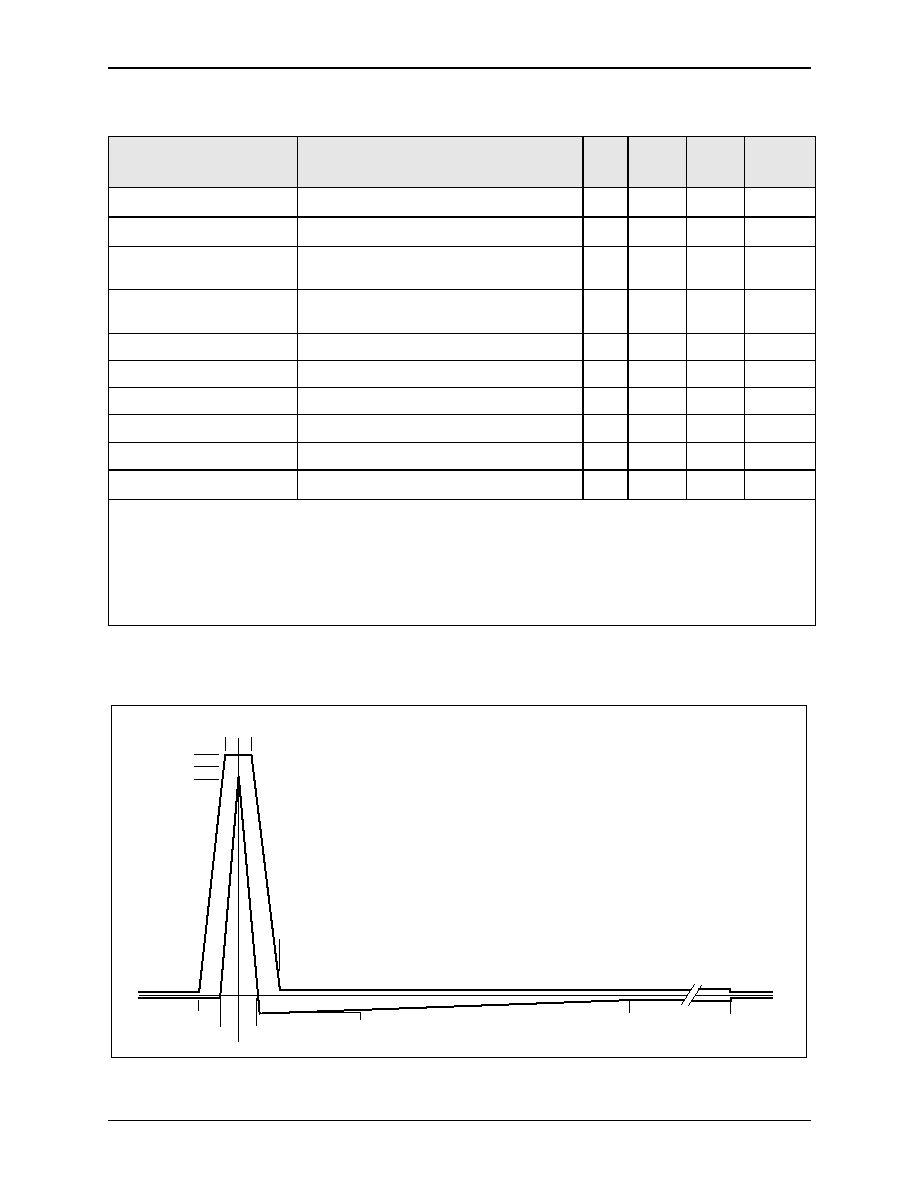
P
rel
im
in
ary
R
evi
ew
5.0 Electrical & Mechanical Specifications
Bt8970
5.6 Microcomputer Interface Timing
Single-Chip HDSL Transceiver
5-18
Conexant
100101B
Preliminary Information/Conexant Proprietary and Confidential
1
1
/29
/
00 10:00 A.M.
Table 5-18. Transmitter Analog Requirements and Specifications
Parameter
Comments
Mi
n
Typ
Max
Units
Transmit Symbol Rate (f
qclk
)
QCLK Frequency (Data Rate/2)
200
--
584
kHz
Pulse Template
(1, 2, 3)
See
Figure 5-13
, R
L
= 135
--
--
--
--
Average Power
(1, 2, 4)
DC to 2xF
QCLK
, R
L
= 135
, 0dB gain setting
13.
4
--
14.0
dBm
Gain Adjustment Step
Controlled by Transmit Gain Register [0x29].
Seven steps above and eight steps below 0 dB.
0.1
7
0.20
0.24
dB
Output Referred Offset Voltage
--
--
25
mV
Output Current
125
--
--
mA
Common-Mode Voltage
VCOMO
VAA/2
--
V
Output Impedance
(1)
DC to 1 MHz
--
--
2
ĺ
Linearity
At Output Symbol Peak
--
0.01
--
%FSR
(5)
Harmonic Distortion
3 kHz, 3.4 V Peak Sine Wave Output, R
L
= 0
--
≠70
--
dB
NOTE(S):
1. Guaranteed by design and characterization.
2. See 5-14 of the Test Conditions section of this datasheet for test circuit.
3. Measured after the transmitter is calibrated by writing the value in the Transmitter Calibration Register [tx_calibrate; 0x28] to
the Transmitter Gain Register [tx_gain; 0x29].
4. Measured with a pseudo-random code sequence of pulses.
5. FSR is Full Scale Range.
Figure 5-13. Transmitted Pulse Template
B = 1.07
C = 1.00
D = 0.93
≠0.4T
0.4T
1.25T
E = 0.03
G = ≠0.16
0.5T
≠0.6T
≠1.2T
A = 0.01
F = ≠0.01
14T
A = 0.01
F = ≠0.01
H = ≠0.05
50T
T = 1/F
QCLK
100101_025

P
rel
im
in
ary
R
evi
ew
Bt8970
5.0 Electrical & Mechanical Specifications
Single-Chip HDSL Transceiver
5.6 Microcomputer Interface Timing
100101B
Conexant
5-19
Preliminary Information/Conexant Proprietary and Confidential
1
1
/29
/
00 10:00 A.M.
5.6.3 Test Conditions
Table 5-19. Transmitted Pulse Template
Normalized Level
Quaternary Symbols
+3
+1
≠1
≠3
A
0.01
0.0264
0.0088
≠0.0088
≠0.0264
B
1.07
2.8248
0.9416
≠0.9416
≠2.8248
C
1.00
2.6400
0.8800
≠0.8800
≠2.6400
D
0.93
2.4552
0.8184
≠0.8184
≠2.4552
E
0.03
0.0792
0.0264
≠0.0264
≠0.0792
F
≠0.01
≠0.0264
≠0.0088
0.0088
0.0264
G
≠0.16
≠0.4224
≠0.1408
0.1408
0.4224
H
≠0.05
≠0.1320
≠0.0440
0.0440
0.1320
Figure 5-14. Transmitter Test Circuit
NOTE(S):
See Table 4-20 for C8 and transformer values.
TXP (71)
TXN (74)
+
+
-
-
TXLDIP (69)
TXLDIN (70)
3.01 k
1 k
1 k
3.01 k
1 k
1 k
TXPSP (67)
TXPSN (68)
C8
Line
Driver
Line
Transformer
+
-
R
L
1:2
+
_
16.2
16.2
100101_026

P
rel
im
in
ary
R
evi
ew
5.0 Electrical & Mechanical Specifications
Bt8970
5.6 Microcomputer Interface Timing
Single-Chip HDSL Transceiver
5-20
Conexant
100101B
Preliminary Information/Conexant Proprietary and Confidential
1
1
/29
/
00 10:00 A.M.
Table 5-20. Transmitter Test Circuit Component Values
Component
Data Rate
784 kbps
1168 kbps
C8
680 pF
470 pF
L (Primary Inductance - Line Side)
3.0 mH
2.0 mH
Figure 5-15. Standard Output Load (Totem Pole and Three-State Outputs)
CL
From
Bt8970
IOL
IOH
1.5 V
100101_027
Figure 5-16. Open-Drain Output Load (IRQ)
From
Bt8970
C
L
I
OD
V
DD2
100101_028

P
rel
im
in
ary
R
evi
ew
Bt8970
5.0 Electrical & Mechanical Specifications
Single-Chip HDSL Transceiver
5.7 Timing Measurements
100101B
Conexant
5-21
Preliminary Information/Conexant Proprietary and Confidential
1
1
/29
/
00 10:00 A.M.
5.7 Timing Measurements
Figure 5-17
illustrates input waveforms. Output waveforms are displayed in
Figures 5-18 and 5-19.
Figure 5-17. Input Waveforms for Timing Tests
3 V
0 V
2.0 V
0.8 V
Input
High
Input
Low
Input
High
Input
Low
100101_029
Figure 5-18. Output Waveforms for Timing Tests
VDD
0 V
2.4 V
0.4 V
Output
High
Output
Low
Output
High
Output
Low
100101_030

P
rel
im
in
ary
R
evi
ew
5.0 Electrical & Mechanical Specifications
Bt8970
5.7 Timing Measurements
Single-Chip HDSL Transceiver
5-22
Conexant
100101B
Preliminary Information/Conexant Proprietary and Confidential
1
1
/29
/
00 10:00 A.M.
Figure 5-19. Output Waveforms for Three-state Enable and Disable Tests
1.7 V
1.3 V
Output
Disabled
Output
Enabled
1.5 V
V
OH
- 0.2 V
V
OL
+ 0.2 V
Output
Disabled
100101_031

P
rel
im
in
ary
R
evi
ew
Bt8970
5.0 Electrical & Mechanical Specifications
Single-Chip HDSL Transceiver
5.8 Mechanical Specifications
100101B
Conexant
5-23
Preliminary Information/Conexant Proprietary and Confidential
1
1
/29
/
00 10:00 A.M.
5.8 Mechanical Specifications
Figure 5-20. 100-Pin Plastic Quad Flat Pack (PQFP)
100101_032

P
rel
im
in
ary
R
evi
ew
5.0 Electrical & Mechanical Specifications
Bt8970
5.8 Mechanical Specifications
Single-Chip HDSL Transceiver
5-24
Conexant
100101B
Preliminary Information/Conexant Proprietary and Confidential
1
1
/29
/
00 10:00 A.M.

Further Information
literature@conexant.com
(800) 854-8099 (North America)
(949) 483-6996 (International)
Printed in USA
World Headquarters
Conexant Systems, Inc.
4311 Jamboree Road
Newport Beach, CA
92660-3007
Phone: (949) 483-4600
Fax 1:
(949) 483-4078
Fax 2:
(949) 483-4391
Americas
U.S. Northwest/
Pacific Northwest ≠ Santa Clara
Phone: (408) 249-9696
Fax:
(408) 249-7113
U.S. Southwest ≠ Los Angeles
Phone: (805) 376-0559
Fax:
(805) 376-8180
U.S. Southwest ≠ Orange County
Phone: (949) 483-9119
Fax:
(949) 483-9090
U.S. Southwest ≠ San Diego
Phone: (858) 713-3374
Fax:
(858) 713-4001
U.S. North Central ≠ Illinois
Phone: (630) 773-3454
Fax:
(630) 773-3907
U.S. South Central ≠ Texas
Phone: (972) 733-0723
Fax:
(972) 407-0639
U.S. Northeast ≠ Massachusetts
Phone: (978) 367-3200
Fax:
(978) 256-6868
U.S. Southeast ≠ North Carolina
Phone: (919) 858-9110
Fax:
(919) 858-8669
U.S. Southeast ≠ Florida/
South America
Phone: (727) 799-8406
Fax:
(727) 799-8306
U.S. Mid-Atlantic ≠ Pennsylvania
Phone: (215) 244-6784
Fax:
(215) 244-9292
Canada ≠ Ontario
Phone: (613) 271-2358
Fax:
(613) 271-2359
Europe
Europe Central ≠ Germany
Phone: +49 89 829-1320
Fax:
+49 89 834-2734
Europe North ≠ England
Phone: +44 1344 486444
Fax:
+44 1344 486555
Europe ≠ Israel/Greece
Phone: +972 9 9524000
Fax:
+972 9 9573732
Europe South ≠ France
Phone: +33 1 41 44 36 51
Fax:
+33 1 41 44 36 90
Europe Mediterranean ≠ Italy
Phone: +39 02 93179911
Fax:
+39 02 93179913
Europe ≠ Sweden
Phone: +46 (0) 8 5091 4319
Fax:
+46 (0) 8 590 041 10
Europe ≠ Finland
Phone: +358 (0) 9 85 666 435
Fax:
+358 (0) 9 85 666 220
Asia ≠ Pacific
Taiwan
Phone: (886-2) 2-720-0282
Fax:
(886-2) 2-757-6760
Australia
Phone: (61-2) 9869 4088
Fax:
(61-2) 9869 4077
China ≠ Central
Phone: 86-21-6361-2515
Fax:
86-21-6361-2516
China ≠ South
Phone: (852) 2 827-0181
Fax:
(852) 2 827-6488
China ≠ South (Satellite)
Phone: (86) 755-5182495
China ≠ North
Phone: (86-10) 8529-9777
Fax:
(86-10) 8529-9778
India
Phone: (91-11) 692-4789
Fax:
(91-11) 692-4712
Korea
Phone: (82-2) 565-2880
Fax:
(82-2) 565-1440
Korea (Satellite)
Phone: (82-53) 745-2880
Fax:
(82-53) 745-1440
Singapore
Phone: (65) 737 7355
Fax:
(65) 737 9077
Japan
Phone: (81-3) 5371 1520
Fax:
(81-3) 5371 1501
www.conexant.com
0.0 Sales Offices