 | –≠–ª–µ–∫—Ç—Ä–æ–Ω–Ω—ã–π –∫–æ–º–ø–æ–Ω–µ–Ω—Ç: CX02048 | –°–∫–∞—á–∞—Ç—å:  PDF PDF  ZIP ZIP |

02048-DSH-001-C
June 2003
P
r
e
l
i
m
i
n
a
r
y
I
n
f
o
r
m
a
t
i
o
n
M02048
Low Power 3.3 Volt Limiting Amplifier
For Data Rates to 3.3 Gbps
Data Sheet
Information provided in this Data Sheet is PRELIMINARY and is subject to change without notice.
Mindspeed TechnologiesTM, Inc, Proprietary and Confidential
Applications Information
Please use this data sheet in conjunction with the technical information:
M02048 Product Bulletin:
02048-PBD-001-B
M02048 Application Note:
02048-APP-001-B
BCC Package Application Note:
AN0004 Rev 01
Bare Die Application Note:
Note 0024 Rev 02

02048-DSH-001-C
Page 2 of 17
M02048
Low Power 3.3 Volt Limiting Amplifier for Data Rates to 3.3 Gbps
P
r
e
l
i
m
i
n
a
r
y
I
n
f
o
r
m
a
t
i
o
n
Information provided in this Data Sheet is PRELIMINARY and is subject to change without notice.
Mindspeed TechnologiesTM, Proprietary and Confidential
T
ABLE
OF
C
ONTENTS
Features ...........................................................................................................................................................3
Applications ......................................................................................................................................................3
Connections ......................................................................................................................................................3
Description ........................................................................................................................................................3
Table 1 Ordering Information ............................................................................................................................3
Top Level Diagram ...........................................................................................................................................3
Table 2 Pin Descriptions ...................................................................................................................................4
Table 3 Absolute Maximum Ratings .................................................................................................................5
Table 4 Recommended Operating Conditions .................................................................................................5
Table 5 DC Characteristics ...............................................................................................................................6
Table 6 AC Characteristics ...............................................................................................................................7
Functional Block Diagram .................................................................................................................................8
Functional Description ......................................................................................................................................8
Overview ...........................................................................................................................................................8
Inputs ................................................................................................................................................................8
Outputs .............................................................................................................................................................8
DC Offset Compensation ..................................................................................................................................8
Signal Level Detector .......................................................................................................................................8
JAM Function ....................................................................................................................................................9
Bias ...................................................................................................................................................................9
RSSI .................................................................................................................................................................9
Applications Circuit (1) 400 mVpp-Diff ..............................................................................................................10
Applications Circuit (2) 800 mVpp - Diff ............................................................................................................10
Applications Information ...................................................................................................................................11
Setting Output Swing Level ..............................................................................................................................11
Output Connection for Maximum AC-Coupled Output Amplitude of 300mV
PP
SE ..........................................11
Setting Signal Detect Level ..............................................................................................................................12
Table 7 Resistor Values ...................................................................................................................................12
Typical Signal Detect Level ..............................................................................................................................12
RSSI Characteristics ........................................................................................................................................12
Package Information .........................................................................................................................................13
Bare Die ............................................................................................................................................................14
Table 8 Pad Coordinates ..................................................................................................................................14
Table 9 Die Information ....................................................................................................................................15
Disclaimer .........................................................................................................................................................16
Contact Information ...........................................................................................................................................17

02048-DSH-001-C
Page 3 of 17
M02048
Low Power 3.3 Volt Limiting Amplifier for Data Rates to 3.3 Gbps
P
r
e
l
i
m
i
n
a
r
y
I
n
f
o
r
m
a
t
i
o
n
Information provided in this Data Sheet is PRELIMINARY and is subject to change without notice.
Mindspeed TechnologiesTM, Proprietary and Confidential
F
EATURES
q
Wide dynamic range with 5 mV input sensitivity at
3.3 Gbps
q
Programmable input signal level detect
q
Fully differential
q
CML data outputs with default <80 ps rise and fall
time
q
Temperature range 0 to +85∞C
q
Operates with +3.3 V supply
q
Supply current typically 26 mA
q
Programmable output amplitude (default 400 mVpp
differential)
q
On-chip DC offset cancellation circuit; no external
capacitors needed
A
PPLICATIONS
q
3.3 Gbps SDH/SONET with FEC
q
2.5 Gbps STM-16/OC-48 SDH/SONET
q
2.12 Gbps Fibre Channel
C
ONNECTIONS
D
ESCRIPTION
The M02048 is an integrated high-gain limiting amplifier
intended for high-speed fiber optics based
communications. Placed following the photodetector and
transimpedance amplifier, the limiting amplifier provides
the necessary gain to ensure full CML output swing even
at minimum input sensitivity.
Capable of operating over a very wide frequency range,
the M02048 supports data rates up to 3.3 Gbps.
The M02048 also includes a programmable signal level
detector, allowing the user to set the threshold at which
the status logic outputs are enabled.
T
ABLE
1
O
RDERING
I
NFORMATION
Please see application note 02048-APP-001-B.
T
OP
L
EVEL
D
IAGRAM
5
9
13
(GND)
1
2
3
4
12
11
10
6
7
8
16
15
14
RSSI
AMPSET
DOUT
DOUT
V
CC
D
V S
E
T
N
/
C
N/C
DIN
DIN
IREF
J
A
M
S
T
S
T
4mm
4
m
m
V
CC
A
V
C
C
A
Fig. 1
BCC++16 Package
Top View
Part Number
Pin Package
M02048DIEWP
Waffle Packed Die
M02048WAFER
Expanded whole wafer on a Grip ring
M02048B16
BCC++16
M02048B16TR
BCC++16 Tape and Reel
M02048-EVM
Evaluation board
AMP
SET
CML
Buffer
Level
Detector
Amplitude
Control
DIN
50
O
50
O
100
O
100
O
DOUT
Threshold
Setting
Circuit
Biasing
JAM
I REF
ST
VSET
ST
DOUT
DIN
R
SSI
V
CC
A
V
CC
D
Limiting
Amplifier
CMOS
Buffer
Comparator
Fig. 2

02048-DSH-001-C
Page 4 of 17
M02048
Low Power 3.3 Volt Limiting Amplifier for Data Rates to 3.3 Gbps
P
r
e
l
i
m
i
n
a
r
y
I
n
f
o
r
m
a
t
i
o
n
Information provided in this Data Sheet is PRELIMINARY and is subject to change without notice.
Mindspeed TechnologiesTM, Proprietary and Confidential
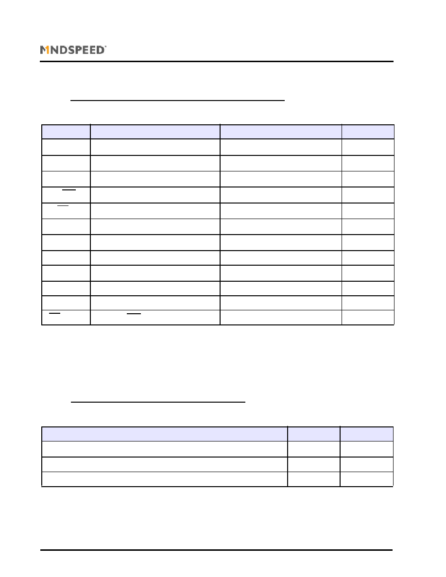
T
ABLE
2
P
IN
D
ESCRIPTIONS
Die Pads
BCC++16
Name
Function
23
1
R
SSI
Receiver signal strength indication. Connect to ground with a 4.7 nF capacitor
(referenced to V
CC
)
1
2
AMP
SET
Enables setting of output voltage swing from 400 mV pp differential to 800 mV pp
differential using an external 1% resistor (R
AMPSET
to ground)
2
-
GNDD
Digital ground
3
-
GNDD
Digital ground
4
3
D
OUT
Inverting differential data output
5
4
D
OUT
Non-inverting differential data output
6
-
GNDD
Digital ground
7
5
V
CC
D
Digital positive supply
8
6
V
CC
A
Analog positive supply
9
-
GNDA
Analog ground
10
7
V
SET
Signal detect threshold setting input. User programmed with 1% resistor (R
SET
) to V
CC
11
-
GNDA
Analog ground
-
8
NC
Not connected
-
9
NC
Not connected
12
10
D
IN
Non-inverting data input
13
11
D
IN
Inverting data input
14
-
GNDA
Analog ground
15
-
GNDA
Analog ground
16
12
V
CC
A
Analog positive supply
17
13
I
REF
This pin generates an on-chip reference current, and must be connected via an external
1% resistor (R
REF
) to ground
18
-
GNDA
Analog ground
19
14
JAM
When HIGH data outputs D
OUT
and D
OUT
are disabled (D
OUT
being held LOW and D
OUT
being held HIGH)
20
15
ST
Logical inverse of ST pin. May be connected to JAM pin to enable automatic jam
function on output. This is an open drain output with an internal 100K
pull-up
21
16
ST
Input signal level status. This output is low when the input signal is below the set
threshold. This is an open drain output with an internal 100K
pull-up
22
-
GNDA
Analog ground
-
Center
GND
Ground. Connect via die-plate
02048-DSH-001-C
Page 5 of 17
M02048
Low Power 3.3 Volt Limiting Amplifier for Data Rates to 3.3 Gbps
P
r
e
l
i
m
i
n
a
r
y
I
n
f
o
r
m
a
t
i
o
n
Information provided in this Data Sheet is PRELIMINARY and is subject to change without notice.
Mindspeed TechnologiesTM, Proprietary and Confidential
T
ABLE
3
A
BSOLUTE
M
AXIMUM
R
ATINGS
These are the absolute maximum ratings at or beyond which the IC can be expected to fail or be damaged. Reliable
operation at these extremes for any length of time is not implied.
Note: The die-plate must be adequately grounded to ensure correct thermal and electrical performance, and it is
recommended that vias are inserted through to a lower ground plane.
T
ABLE
4
R
ECOMMENDED
O
PERATING
C
ONDITIONS
Symbol
Parameter
Rating
Units
V
CC
Power supply voltage (V
CC
-GND)
-0.5 to +6V
V
T
A
Operating ambient temperature
0 to +85
∞C
T
STG
Storage temperature
-65 to +150
∞C
D
OUT
, D
OUT
Output pins voltage
V
CC
- 0.4 to V
CC
+ 0.4
V
D
IN
, D
IN
Data input pins voltage
V
CC
- 0.32 to V
CC
+ 0.32
V
AMP
SET
Output amplitude setting pin voltage
GND to +0.1
V
V
SET
Signal detect threshold setting pin voltage
GND to +3.6
V
JAM
Output enable pin voltage
GND to +3.6
V
I
REF
Current into Reference input
+ 0 to -120
µA
RSSI
RSSI pin voltage
+1 to +3.6
V
I(ST)
Current into Status pin
+1500 to -100
µA
I(ST)
Current into Status pin
+1500 to -100
µA
Parameter
Rating
Units
Power supply (V
CC
-GND)
3.3 ± 10%
V
Junction temperature
0 to +110
∞C
Operating ambient
0 to +85
∞C