
Single/Dual/Triple E3/DS3/STS-1
Line Interface Unit
Data Sheet
CX28331/CX28332/CX28333 (≠1x)
28333-DSH-001-A
Feb 2003

© 2002, 2003
Mindspeed TechnologiesTM, a Conexant business
All Rights Reserved.
Information in this document is provided in connection with Mindspeed Technologies ("Mindspeed") products. These materials are provided by
Mindspeed as a service to its customers and may be used for informational purposes only. Mindspeed assumes no responsibility for errors or
omissions in these materials. Mindspeed may make changes to specifications and product descriptions at any time, without notice. Mindspeed
makes no commitment to update the information and shall have no responsibility whatsoever for conflicts or incompatibilities arising from future
changes to its specifications and product descriptions.
No license, express or implied, by estoppel or otherwise, to any intellectual property rights is granted by this document. Except as provided in
Mindspeed's Terms and Conditions of Sale for such products, Mindspeed assumes no liability whatsoever.
THESE MATERIALS ARE PROVIDED "AS IS" WITHOUT WARRANTY OF ANY KIND, EITHER EXPRESS OR IMPLIED, RELATING TO
SALE AND/OR USE OF MINDSPEED PRODUCTS INCLUDING LIABILITY OR WARRANTIES RELATING TO FITNESS FOR A
PARTICULAR PURPOSE, CONSEQUENTIAL OR INCIDENTAL DAMAGES, MERCHANTABILITY, OR INFRINGEMENT OF ANY PATENT,
COPYRIGHT OR OTHER INTELLECTUAL PROPERTY RIGHT. MINDSPEED FURTHER DOES NOT WARRANT THE ACCURACY OR
COMPLETENESS OF THE INFORMATION, TEXT, GRAPHICS OR OTHER ITEMS CONTAINED WITHIN THESE MATERIALS. MINDSPEED
SHALL NOT BE LIABLE FOR ANY SPECIAL, INDIRECT, INCIDENTAL, OR CONSEQUENTIAL DAMAGES, INCLUDING WITHOUT
LIMITATION, LOST REVENUES OR LOST PROFITS, WHICH MAY RESULT FROM THE USE OF THESE MATERIALS.
Mindspeed products are not intended for use in medical, lifesaving or life sustaining applications. Mindspeed customers using or selling
Mindspeed products for use in such applications do so at their own risk and agree to fully indemnify Mindspeed for any damages resulting from
such improper use or sale.
The following are trademarks of Conexant Systems, Inc.: Mindspeed TechnologiesTM, the MindspeedTM logo, and "Build It First"TM. Product
names or services listed in this publication are for identification purposes only, and may be trademarks of third parties. Third-party brands and
names are the property of their respective owners.
For additional disclaimer information, please consult Mindspeed Technologies Legal Information posted at
www.mindspeed.com
which is
incorporated by reference.
28333-DSH-001-A
Mindspeed Technologies
TM
Mindspeed Proprietary and Confidential
Revision History
Revision
Level
Date
Description
A
--
2/2003
Initial Release [Document number 28333-DSH-001-A]
Updated LBO to 450 feet
Incorporated Errata #500371A
Removed CX2833i-3x information (see prior document)
Removed EVM, IBIS, and JAT Appendices
Fixed description of transmit AIS during loopback
operations
Added loopback diagrams
Updated PCB design considerations
Added power sequencing requirements
General corrections

28333-DSH-001-A
Mindspeed Technologies
TM
iii
Mindspeed Proprietary and Confidential
CX28331/CX28332/CX28333 (≠1x)
Single/Dual/Triple E3/DS3/STS-1 Line Interface Unit
The CX28333 is a three-channel, DS3/E3/STS-1, fully integrated Line Interface Unit
(LIU) device. It is configured via external pins and does not require a microprocessor
interface. Each channel has an independent receive equalizer requiring no user
configuration. Additionally, each channel has a programmable transmit pulse shaper
that can be set to ensure that the transmit pulse meets the pulse mask requirement
for the digital cross-connect. The CX28332 is a dual-channel, and the CX28331 is a
single-channel LIU with performance identical to the CX28333.
The CX28333 gives the user new economies of scale in concentrator applications
where three DS3 or STS-1 channels
are concentrated into a single STS-3 channel.
Each line interface is reduced to 1:1 coupling transformers, terminating resistors, and
a capacitor.
NOTE:
In this document, "i" is used to represent the number of channels:
i = 1 (CX28331), i = 2 (CX28332), and i = 3 (CX28333).
Functional Block Diagram
TPOS
TNEG
TCLK
ENCODER
TAIS
Pulse
Shaper
E3MODE
LINE
DRIVER
PDB
DATA
MUX
RLOOP
ENDECDIS
LLOOP
LBO
XOE
TLINEP
TLINEM/N
DECODER
RPOS
RNEG
RCLK
RLOS
TCLK
Clock/
Data
Recovery
PDATA
PDATA/
NDATA
NDATA
DATCLK
P
N Receiver
ALOS
RLINEP
RLINEM/N
REFCLK
REQH
Channel 1
Channel 2
Channel 3
Distinguishing Features
∑
Programmable pulse shaper to meet
cross-connect pulse masks (ANSI T1.102-
1993)
∑
Meets jitter tolerance and jitter generation
specifications of Bellcore GR499, GR253
and ETSI TBR24
∑
Alarms for coding violation and loss of
signal
∑
Full diagnostic loopback capability
∑
Uses a minimum of external components
∑
Compliant with ITU-G.703 and ETSI
TBR24
∑
Independent power down mode per
channel
∑
Easily interfaced to the DS3/E3 Framer IC
(CX28342/3/4/6/8 and CN8330)
∑
Selectable B3ZS/HDB3 encoding/
decoding
Physical Characteristics
∑
80-pin ETQFP package
∑
Single 3.3 V power supply
∑
1 W maximum power dissipation
(CX28333)
∑
- 40 ∞C to +85 ∞C temperature range
∑
5 V-tolerant pins
∑
TTL digital pins
Applications
∑
Digital Cross-Connect Systems
∑
Routers
∑
ATM Switches
∑
Channelized Line Aggregation Units
∑
Test Equipment
∑
Channel Service Units
∑
Multiplexers

iv
Mindspeed Technologies
TM
28333-DSH-001-A
Mindspeed Proprietary and Confidential
CX28333EVM
Ordering Information
Model Number
Package
Description
Operating Temperature
CX28331-1x
80-Pin ETQFP
Single-channel LIU
≠40 ∞C to +85 ∞C
CX28332-1x
80-Pin ETQFP
Dual-channel LIU
≠40 ∞C to +85 ∞C
CX28333-1x
80-Pin ETQFP
Triple-channel LIU
≠40 ∞C to +85 ∞C
CH2
CH3
CX28333
NRZTX DATA and CLK in
Loss of Signal
Code Violation
Clock Input
Control
TX B3ZS/HDB3 analog out
RX B3ZS/HDB3 analog in
NRZRX DATA and CLK out
NRZTX DATA and CLK in
NRZRX DATA and CLK out
NRZTX DATA and CLK in
NRZRX DATA and CLK out
CH1
CH2
CH3
CH1
TX B3ZS/HDB3 analog out
RX B3ZS/HDB3 analog in
TX B3ZS/HDB3 analog out
RX B3ZS/HDB3 analog in
L
I
N
E
S
I
D
E
F
R
A
M
E
R
S
I
D
E
100985_002

28333-DSH-001-A
Mindspeed Technologies
TM
v
Mindspeed Proprietary and Confidential
Table of Contents
Table of Contents
. . . . . . . . . . . . . . . . . . . . . . . . . . . . . . . . . . . . . . . . . . . . . . . . . . . . . . . . . . . . . . . v
List of Figures
. . . . . . . . . . . . . . . . . . . . . . . . . . . . . . . . . . . . . . . . . . . . . . . . . . . . . . . . . . . . . . . . .
vii
List of Tables
. . . . . . . . . . . . . . . . . . . . . . . . . . . . . . . . . . . . . . . . . . . . . . . . . . . . . . . . . . . . . . . . . .
ix
1.0
Pin Description
. . . . . . . . . . . . . . . . . . . . . . . . . . . . . . . . . . . . . . . . . . . . . . . . . . . . . . . . . . . . . . . . . 1-1
1.1
Pin Assignments
. . . . . . . . . . . . . . . . . . . . . . . . . . . . . . . . . . . . . . . . . . . . . . . . . . . . . . . . . . . . 1-1
2.0
Functional Description
. . . . . . . . . . . . . . . . . . . . . . . . . . . . . . . . . . . . . . . . . . . . . . . . . . . . . . . . . . 2-1
2.1
Overview
. . . . . . . . . . . . . . . . . . . . . . . . . . . . . . . . . . . . . . . . . . . . . . . . . . . . . . . . . . . . . . . . . . 2-1
2.2
Transmitter
. . . . . . . . . . . . . . . . . . . . . . . . . . . . . . . . . . . . . . . . . . . . . . . . . . . . . . . . . . . . . . . . 2-3
2.2.1
AMI B3ZS/HDB3 Encoder
. . . . . . . . . . . . . . . . . . . . . . . . . . . . . . . . . . . . . . . . . . . . . . . . 2-3
2.2.2
Pulse Shaper
. . . . . . . . . . . . . . . . . . . . . . . . . . . . . . . . . . . . . . . . . . . . . . . . . . . . . . . . . 2-3
2.2.3
Line Driver
. . . . . . . . . . . . . . . . . . . . . . . . . . . . . . . . . . . . . . . . . . . . . . . . . . . . . . . . . . . 2-4
2.2.3.1
Transmit Pulse Mask Templates
. . . . . . . . . . . . . . . . . . . . . . . . . . . . . . . . . . . 2-5
2.2.4
Alarm Indication Signal (AIS) Generator
. . . . . . . . . . . . . . . . . . . . . . . . . . . . . . . . . . . . . 2-8
2.2.5
Jitter Generation (Intrinsic)
. . . . . . . . . . . . . . . . . . . . . . . . . . . . . . . . . . . . . . . . . . . . . . . 2-8
2.3
Receiver
. . . . . . . . . . . . . . . . . . . . . . . . . . . . . . . . . . . . . . . . . . . . . . . . . . . . . . . . . . . . . . . . . . 2-9
2.3.1
Receive Sensitivity
. . . . . . . . . . . . . . . . . . . . . . . . . . . . . . . . . . . . . . . . . . . . . . . . . . . . . 2-9
2.3.2
AGC/VGA Block
. . . . . . . . . . . . . . . . . . . . . . . . . . . . . . . . . . . . . . . . . . . . . . . . . . . . . . . 2-9
2.3.3
Receive Equalizer
. . . . . . . . . . . . . . . . . . . . . . . . . . . . . . . . . . . . . . . . . . . . . . . . . . . . . . 2-9
2.3.4
The PLL Clock Recovery Circuit
. . . . . . . . . . . . . . . . . . . . . . . . . . . . . . . . . . . . . . . . . . 2-10
2.3.5
Loss Of Signal (LOS) Detector
. . . . . . . . . . . . . . . . . . . . . . . . . . . . . . . . . . . . . . . . . . . 2-10
2.3.6
B3ZS/HDB3 Decoder With Bipolar Violation Detector
. . . . . . . . . . . . . . . . . . . . . . . . . . . 2-10
2.3.7
Data Squelching
. . . . . . . . . . . . . . . . . . . . . . . . . . . . . . . . . . . . . . . . . . . . . . . . . . . . . . 2-11
2.4
Jitter Tolerance
. . . . . . . . . . . . . . . . . . . . . . . . . . . . . . . . . . . . . . . . . . . . . . . . . . . . . . . . . . . . 2-11
2.4.1
Jitter Transfer
. . . . . . . . . . . . . . . . . . . . . . . . . . . . . . . . . . . . . . . . . . . . . . . . . . . . . . . . 2-13
2.5
Additional CX2833i Functions
. . . . . . . . . . . . . . . . . . . . . . . . . . . . . . . . . . . . . . . . . . . . . . . . . 2-14
2.5.1
Bias Generator
. . . . . . . . . . . . . . . . . . . . . . . . . . . . . . . . . . . . . . . . . . . . . . . . . . . . . . . 2-14
2.5.2
Power-On Reset (POR)
. . . . . . . . . . . . . . . . . . . . . . . . . . . . . . . . . . . . . . . . . . . . . . . . . 2-14
2.5.3
Loopback Multiplexers (MUXes)
. . . . . . . . . . . . . . . . . . . . . . . . . . . . . . . . . . . . . . . . . . 2-14
2.6
Mechanical Specifications
. . . . . . . . . . . . . . . . . . . . . . . . . . . . . . . . . . . . . . . . . . . . . . . . . . . 2-17

Table of Contents
CX28331/CX28332/CX28333 (-1x)
Single/Dual/Triple E3/DS3/STS-1 Line Interface Unit
vi
Mindspeed Technologies
TM
28333-DSH-001-A
Mindspeed Proprietary and Confidential
2.7
Electrical Characteristics
. . . . . . . . . . . . . . . . . . . . . . . . . . . . . . . . . . . . . . . . . . . . . . . . . . . . 2-18
2.7.1
Absolute Maximum Ratings
. . . . . . . . . . . . . . . . . . . . . . . . . . . . . . . . . . . . . . . . . . . . . 2-18
2.7.2
ESD Ratings
. . . . . . . . . . . . . . . . . . . . . . . . . . . . . . . . . . . . . . . . . . . . . . . . . . . . . . . . . 2-19
2.7.3
Recommended Operating Conditions
. . . . . . . . . . . . . . . . . . . . . . . . . . . . . . . . . . . . . . 2-19
2.8
DC Characteristics
. . . . . . . . . . . . . . . . . . . . . . . . . . . . . . . . . . . . . . . . . . . . . . . . . . . . . . . . . 2-20
2.9
AC Characteristics
. . . . . . . . . . . . . . . . . . . . . . . . . . . . . . . . . . . . . . . . . . . . . . . . . . . . . . . . . . 2-21
3.0
Applications
. . . . . . . . . . . . . . . . . . . . . . . . . . . . . . . . . . . . . . . . . . . . . . . . . . . . . . . . . . . . . . . . . . . 3-1
3.1
PCB Design Considerations for the CX2833i
. . . . . . . . . . . . . . . . . . . . . . . . . . . . . . . . . . . . . . . 3-1
3.1.1
Power Supply and Ground Plane
. . . . . . . . . . . . . . . . . . . . . . . . . . . . . . . . . . . . . . . . . . . 3-1
3.1.2
Component Placement
. . . . . . . . . . . . . . . . . . . . . . . . . . . . . . . . . . . . . . . . . . . . . . . . . . 3-1
3.1.2.1
RBIAS Resistor
. . . . . . . . . . . . . . . . . . . . . . . . . . . . . . . . . . . . . . . . . . . . . . . 3-1
3.1.2.2
VGG Decoupling
. . . . . . . . . . . . . . . . . . . . . . . . . . . . . . . . . . . . . . . . . . . . . . 3-2
3.1.2.3
Termination Resistors and Capacitors
. . . . . . . . . . . . . . . . . . . . . . . . . . . . . . 3-2
3.1.3
Impedance Matching
. . . . . . . . . . . . . . . . . . . . . . . . . . . . . . . . . . . . . . . . . . . . . . . . . . . 3-2
3.1.4
Other Passive Parts
. . . . . . . . . . . . . . . . . . . . . . . . . . . . . . . . . . . . . . . . . . . . . . . . . . . . 3-2
3.1.5
IBIS Models
. . . . . . . . . . . . . . . . . . . . . . . . . . . . . . . . . . . . . . . . . . . . . . . . . . . . . . . . . . 3-2
3.1.6
Recommended Vendors
. . . . . . . . . . . . . . . . . . . . . . . . . . . . . . . . . . . . . . . . . . . . . . . . . 3-3
Appendix A:Applicable Standards
. . . . . . . . . . . . . . . . . . . . . . . . . . . . . . . . . . . . . . . . . . . . . . . . . . . . . . A-1
Appendix B: Exposed Thin Quad Flat (ETQFP) Pack
. . . . . . . . . . . . . . . . . . . . . . . . . . . . . . . . . . . . . . B-1
B.1
Introduction
. . . . . . . . . . . . . . . . . . . . . . . . . . . . . . . . . . . . . . . . . . . . . . . . . . . . . . . . . . . . . . . B-2
B.2
Package Thermal Characterization
. . . . . . . . . . . . . . . . . . . . . . . . . . . . . . . . . . . . . . . . . . . . . . B-3
B.2.1
Heat Removal Path
. . . . . . . . . . . . . . . . . . . . . . . . . . . . . . . . . . . . . . . . . . . . . . . . . . . . B-3
B.2.2
Thermal Lands
. . . . . . . . . . . . . . . . . . . . . . . . . . . . . . . . . . . . . . . . . . . . . . . . . . . . . . . B-3
B.2.3
PCB Design
. . . . . . . . . . . . . . . . . . . . . . . . . . . . . . . . . . . . . . . . . . . . . . . . . . . . . . . . . B-5
B.2.4
Thermal Test Structure
. . . . . . . . . . . . . . . . . . . . . . . . . . . . . . . . . . . . . . . . . . . . . . . . . B-6
B.2.4.1
Test Environment
. . . . . . . . . . . . . . . . . . . . . . . . . . . . . . . . . . . . . . . . . . . . B-6
B.2.4.2
Thermal Test Boards
. . . . . . . . . . . . . . . . . . . . . . . . . . . . . . . . . . . . . . . . . . B-6
B.2.5
Package Thermal Performance
. . . . . . . . . . . . . . . . . . . . . . . . . . . . . . . . . . . . . . . . . . . B-7
B.2.5.1
Calculation Guidelines
. . . . . . . . . . . . . . . . . . . . . . . . . . . . . . . . . . . . . . . . . B-7
B.2.5.2
Package Thermal Resistance
. . . . . . . . . . . . . . . . . . . . . . . . . . . . . . . . . . . . B-7
B.3
Solder Stencil Determination
. . . . . . . . . . . . . . . . . . . . . . . . . . . . . . . . . . . . . . . . . . . . . . . . . . B-9
B.4
Solder Reflow Profile
. . . . . . . . . . . . . . . . . . . . . . . . . . . . . . . . . . . . . . . . . . . . . . . . . . . . . . . . B-9
Appendix C: Power Sequencing
. . . . . . . . . . . . . . . . . . . . . . . . . . . . . . . . . . . . . . . . . . . . . . . . . . . . . . . . C-1

CX28331/CX28332/CX28333 (-1x)
List of Figures
Single/Dual/Triple E3/DS3/STS-1 Line Interface Unit
28333-DSH-001-A
Mindspeed Technologies
TM
vii
Mindspeed Proprietary and Confidential
List of Figures
Figure 1-1.
CX28331-1x Pin Diagram . . . . . . . . . . . . . . . . . . . . . . . . . . . . . . . . . . . . . . . . . . . . . . . . . . 1-2
Figure 1-2.
CX28332-1x Pin Diagram . . . . . . . . . . . . . . . . . . . . . . . . . . . . . . . . . . . . . . . . . . . . . . . . . . 1-3
Figure 1-3.
CX28333-1x Pin Diagram . . . . . . . . . . . . . . . . . . . . . . . . . . . . . . . . . . . . . . . . . . . . . . . . . . 1-4
Figure 2-1.
Typical Application Of Single CX2833i Channel . . . . . . . . . . . . . . . . . . . . . . . . . . . . . . . . . . 2-2
Figure 2-2.
Pulse Shaper . . . . . . . . . . . . . . . . . . . . . . . . . . . . . . . . . . . . . . . . . . . . . . . . . . . . . . . . . . . . 2-3
Figure 2-3.
Pulse Measurement Points . . . . . . . . . . . . . . . . . . . . . . . . . . . . . . . . . . . . . . . . . . . . . . . . . 2-4
Figure 2-4.
Transmit Pulse Mask for DS3 Rates . . . . . . . . . . . . . . . . . . . . . . . . . . . . . . . . . . . . . . . . . . 2-5
Figure 2-5.
Transmit Pulse Mask for STS-1 Rates . . . . . . . . . . . . . . . . . . . . . . . . . . . . . . . . . . . . . . . . . 2-6
Figure 2-6.
Transmit Pulse Mask for E3 Rate. . . . . . . . . . . . . . . . . . . . . . . . . . . . . . . . . . . . . . . . . . . . . 2-7
Figure 2-7.
AIS Signal . . . . . . . . . . . . . . . . . . . . . . . . . . . . . . . . . . . . . . . . . . . . . . . . . . . . . . . . . . . . . . 2-8
Figure 2-8.
Minimum Jitter Tolerance Requirement. . . . . . . . . . . . . . . . . . . . . . . . . . . . . . . . . . . . . . . 2-12
Figure 2-9.
Maximum Jitter Transfer Curve Requirement . . . . . . . . . . . . . . . . . . . . . . . . . . . . . . . . . . 2-13
Figure 2-10.
Remote Loopback Diagram . . . . . . . . . . . . . . . . . . . . . . . . . . . . . . . . . . . . . . . . . . . . . . . . 2-15
Figure 2-11.
Local Loopback Diagram. . . . . . . . . . . . . . . . . . . . . . . . . . . . . . . . . . . . . . . . . . . . . . . . . . 2-16
Figure 2-12.
CX2833i-1x Mechanical Drawing (80-Pin)--Dimensions . . . . . . . . . . . . . . . . . . . . . . . . . 2-17
Figure 2-13.
Timing Diagram. . . . . . . . . . . . . . . . . . . . . . . . . . . . . . . . . . . . . . . . . . . . . . . . . . . . . . . . . 2-22
Figure 3-1.
DS3/E3 Application Diagram . . . . . . . . . . . . . . . . . . . . . . . . . . . . . . . . . . . . . . . . . . . . . . . . 3-4
Figure B-1.
Schematic Representation of the Package Components . . . . . . . . . . . . . . . . . . . . . . . . . . . B-2
Figure B-2.
Package and PCB Land Configuration . . . . . . . . . . . . . . . . . . . . . . . . . . . . . . . . . . . . . . . . . B-3
Figure B-3.
Internal Structure for a Two-Layer PCB . . . . . . . . . . . . . . . . . . . . . . . . . . . . . . . . . . . . . . . . B-5
Figure B-4.
Internal Structure For a Six-Layer PCB . . . . . . . . . . . . . . . . . . . . . . . . . . . . . . . . . . . . . . . . B-5
Figure B-5.
Test Performance Structure (A = 100 mm, B = 100 mm, L
P
= 1.40 mm, L
B
= 1.60 mm) . . B-6
Figure B-6.
Package Thermal Resistance as a Function of Airflow Velocity for a 48-ETQFP Package . . B-7
Figure B-7.
Package Thermal Resistance as a Function of Airflow Velocity for an 64 ETQFP. . . . . . . . . B-8
Figure B-8.
Package Thermal Resistance as a Function of Airflow Velocity for an 80 ETQFP. . . . . . . . . B-8
Figure B-9.
Typical IR Reflow Profile for Eutectic Sn63:Pb37 . . . . . . . . . . . . . . . . . . . . . . . . . . . . . . . B-10
Figure B-10.
Typical Forced Convection Reflow Profile for Eutectic Sn63:Pb37 . . . . . . . . . . . . . . . . . . B-11
Figure C-1.
Power -up sequence of VGG and VDD. . . . . . . . . . . . . . . . . . . . . . . . . . . . . . . . . . . . . . . . . C-1
Figure C-2.
Power-down sequence of VGG and VDD. . . . . . . . . . . . . . . . . . . . . . . . . . . . . . . . . . . . . . . C-1

List of Figures
CX28331/CX28332/CX28333 (-1x)
Single/Dual/Triple E3/DS3/STS-1 Line Interface Unit
viii
Mindspeed Technologies
TM
28333-DSH-001-A
Mindspeed Proprietary and Confidential

CX28331/CX28332/CX28333 (-1x)
List of Tables
Single/Dual/Triple E3/DS3/STS-1 Line Interface Unit
28333-DSH-001-A
Mindspeed Technologies
TM
ix
Mindspeed Proprietary and Confidential
List of Tables
Table 1-1.
CX2833i-1x Pin Definitions . . . . . . . . . . . . . . . . . . . . . . . . . . . . . . . . . . . . . . . . . . . . . . . . . . 1-5
Table 2-1.
DS3 Transmit Template Specifications . . . . . . . . . . . . . . . . . . . . . . . . . . . . . . . . . . . . . . . . . 2-5
Table 2-2.
STS-1 Transmit Template Specifications . . . . . . . . . . . . . . . . . . . . . . . . . . . . . . . . . . . . . . . . 2-6
Table 2-3.
RLOS Threshold Settings . . . . . . . . . . . . . . . . . . . . . . . . . . . . . . . . . . . . . . . . . . . . . . . . . . 2-10
Table 2-4.
Absolute Maximum Ratings . . . . . . . . . . . . . . . . . . . . . . . . . . . . . . . . . . . . . . . . . . . . . . . . 2-18
Table 2-5.
ESD Ratings . . . . . . . . . . . . . . . . . . . . . . . . . . . . . . . . . . . . . . . . . . . . . . . . . . . . . . . . . . . . 2-19
Table 2-6.
Recommended Operating Conditions . . . . . . . . . . . . . . . . . . . . . . . . . . . . . . . . . . . . . . . . . 2-19
Table 2-7.
DC Characteristics. . . . . . . . . . . . . . . . . . . . . . . . . . . . . . . . . . . . . . . . . . . . . . . . . . . . . . . . 2-20
Table 2-8.
AC Characteristics (Logic Timing) . . . . . . . . . . . . . . . . . . . . . . . . . . . . . . . . . . . . . . . . . . . . 2-21
Table B-1.
Dimensional Parameters (mm) . . . . . . . . . . . . . . . . . . . . . . . . . . . . . . . . . . . . . . . . . . . . . . . B-4
Table B-2.
Specification for a Two-Layer Test Board . . . . . . . . . . . . . . . . . . . . . . . . . . . . . . . . . . . . . . . B-6
Table B-3.
Specification for a Four-Layer Test Board . . . . . . . . . . . . . . . . . . . . . . . . . . . . . . . . . . . . . . . B-6
Table B-4.
Specification for Delco Thermal Test Chips . . . . . . . . . . . . . . . . . . . . . . . . . . . . . . . . . . . . . . B-7
Table B-5.
Test Conditions . . . . . . . . . . . . . . . . . . . . . . . . . . . . . . . . . . . . . . . . . . . . . . . . . . . . . . . . . . . B-8

List of Tables
CX28331/CX28332/CX28333 (-1x)
Single/Dual/Triple E3/DS3/STS-1 Line Interface Unit
x
Mindspeed Technologies
TM
28333-DSH-001-A
Mindspeed Proprietary and Confidential

28333-DSH-001-A
Mindspeed Technologies
TM
1-1
Mindspeed Proprietary and Confidential
1
1.0 Pin Description
1.1 Pin Assignments
Figures 1-1
(CX28331-1x),
1-2
(CX28332-1x), and
1-3
(CX28333-1x) illustrate
pin assignments for the 80-pin Exposed Thin Quad Flat Package (ETQFP). See
Table 1-1
for the CX2833i-1x pin descriptions.
The input/output (I/O) column is coded as follows:
I = Input
O = Output
I/O = Bidirectional
P = Power
NOTE:
All digital inputs and outputs contain 75 k
pull-down resistors.
When a channel is disabled (i.e., the PDx pin is tied low or not connected), all
receive and transmit analog circuitry powers down. Analog inputs (RLINE) are
ignored and analog outputs (TLINE) are high impedance. Digital inputs of a
powered-down channel are still active, but ignored. Overall noise on the device
can be lowered by not driving the digital inputs of a powered-down channel.
NOTE:
When power is disconnected from the device, TLINE pins are low
impedance to ground if driven by more than one forward-bias diode
voltage (0.7 V) below ground. Additionally, driving TLINE, a
forward-bias diode voltage above the VGG pin, creates a low impedance
path from the TLINE pin to the VGG pin. Otherwise, the TLINE pins are
high impedance.

1.0 Pin Description
CX28331/CX28332/CX28333 (-1x)
1.1 Pin Assignments
Single/Dual/Triple E3/DS3/STS-1 Line Interface Unit
1-2
Mindspeed Technologies
TM
28333-DSH-001-A
Mindspeed Proprietary and Confidential
Figure 1-1. CX28331-1x Pin Diagram
CX28331-1x
76
77
78
79
80
NC
GPD
RESET
VGG
RBIAS
71
72
73
74
75
NC
NC
DVDDIO
NC
NC
66
67
68
69
70
NC
NC
NC
NC
NC
61
62
63
64
65
NC
NC
NC
NC
NC
56
57
58
59
60
L L O O P
R L O O P
PD
ENDECDIS
D V D D C
51
52
53
54
55
TAIS
R L O S
R C L K
RPOS/RNRZ
RNEG/RLCV
46
47
48
49
50
REQH
R E F C L K
T C L K
TPOS/TNRZ
TNEG/NC
41
42
43
44
45
DVSSC
N C
E 3 M O D E
L B O
XOE
5
4
3
2
1
10
9
8
7
6
15
14
13
12
11
20
19
18
17
16
25
24
23
22
21
NC
VSS
NC
NC
VDD
30
29
28
27
26
NC
NC
DVSSIO
NC
NC
35
34
33
32
31
NC
NC
NC
NC
NC
40
39
38
37
36
NC
NC
NC
NC
NC
RVSS
RLINEN
RLINEP
RVDD
V D D
NC
NC
VSS
TVDD
TLINEN
TLINEP
TVSS
VSS
V D D
NC
NC
VSS
NC
V D D
NC
100985_003

CX28331/CX28332/CX28333 (-1x)
1.0 Pin Description
Single/Dual/Triple E3/DS3/STS-1 Line Interface Unit
1.1 Pin Assignments
28333-DSH-001-A
Mindspeed Technologies
TM
1-3
Mindspeed Proprietary and Confidential
Figure 1-2. CX28332-1x Pin Diagram
CX28332-1x
76
77
78
79
80
PD1
GPD
RESET
VGG
RBIAS
71
72
73
74
75
XOE1
LBO1
DVDDIO
LLOOP1
RLOOP1
66
67
68
69
70
RLOS1
RCLK1
RPOS1/RNRZ1
RNEG1/RLCV1
REQH1
61
62
63
64
65
TAIS1
TCLK1
TPOS1/TNRZ1
TNEG1/NC1
REFCLK1
56
57
58
59
60
NC
NC
NC
NC
NC
NC
NC
NC
NC
NC
NC
NC
NC
NC
NC
E3MODE
ENDECDIS
D V D D C
51
52
53
54
55
46
47
48
49
50
41
42
43
44
45
DVSSC
N C
5
4
3
2
1
10
9
8
7
6
15
14
13
12
11
20
19
18
17
16
25
24
23
22
21
PD2
RVSS2
RLINE2N
RLINE2P
RVDD2
30
29
28
27
26
XOE2
LBO2
DVSSIO
LLOOP2
RLOOP2
35
34
33
32
31
RLOS2
RCLK2
RPOS2/RNRZ2
RNEG2/RLCV2
REQH2
40
39
38
37
36
TAIS2
TNEG2/NC2
TPOS2/TNRZ2
TCLK2
REFCLK2
T V D D 2
TLINE2N
TLINE2P
TVSS2
VSS
NC
NC
VDD
VDD
NC
NC
VSS
TVSS1
T V D D 1
TLINE1N
TLINE1P
RVSS1
RLINE1P
R V D D 1
RLINE1N
100985_004

1.0 Pin Description
CX28331/CX28332/CX28333 (-1x)
1.1 Pin Assignments
Single/Dual/Triple E3/DS3/STS-1 Line Interface Unit
1-4
Mindspeed Technologies
TM
28333-DSH-001-A
Mindspeed Proprietary and Confidential
Figure 1-3. CX28333-1x Pin Diagram
CX28333-1x
76
77
78
79
80
PD1
GPD
RESET
VGG
RBIAS
71
72
73
74
75
XOE1
LBO1
DVDDIO
LLOOP1
RLOOP1
66
67
68
69
70
RLOS1
RCLK1
RPOS1/RNRZ1
RNEG1/RLCV1
REQH1
61
62
63
64
65
TAIS1
TCLK1
TPOS1/TNRZ1
TNEG1/NC1
REFCLK1
56
57
58
59
60
L L O O P 2
R L O O P 2
PD2
ENDECDIS
D V D D C
51
52
53
54
55
TAIS2
R L O S 2
R C L K 2
RPOS2/RNRZ2
RNEG2/RLCV2
46
47
48
49
50
REQH2
R E F C L K 2
T C L K 2
TPOS2/TNRZ2
TNEG2/NC2
41
42
43
44
45
DVSSC
E 3 M O D E
N C
L B O 2
XOE2
5
4
3
2
1
10
9
8
7
6
15
14
13
12
11
20
19
18
17
16
25
24
23
22
21
PD3
RVSS3
RLINE3N
RLINE3P
RVDD3
30
29
28
27
26
XOE3
LBO3
DVSSIO
LLOOP3
RLOOP3
35
34
33
32
31
RLOS3
RCLK3
RPOS3/RNRZ3
RNEG3/RLCV3
REQH3
40
39
38
37
36
TAIS3
TNEG3/NC3
TPOS3/TNRZ3
TCLK3
REFCLK3
RVSS2
RLINE2N
RLINE2P
R V D D 2
T V D D 3
TLINE3N
TLINE3P
TVSS3
T V D D 2
TLINE2N
TLINE2P
TVSS2
TVSS1
T V D D 1
TLINE1N
TLINE1P
RVSS1
RLINE1P
R V D D 1
RLINE1N
100985_005

CX28331/CX28332/CX28333 (-1x)
1.0 Pin Description
Single/Dual/Triple E3/DS3/STS-1 Line Interface Unit
1.1 Pin Assignments
28333-DSH-001-A
Mindspeed Technologies
TM
1-5
Mindspeed Proprietary and Confidential
Table 1-1. CX2833i-1x Pin Definitions (1 of 7)
Pin #
Signal Name
Description
I/O/P
Notes
CX28331-1x CX28332-1x CX28333-1x
Coaxial Line Pins
14
--
--
RLINEP
Ch1 positive receive
data
I
Differential inputs for each channel
from its respective receive coax
line. The RX expects balanced
differential inputs, usually achieved
using a 1:1 transformer.
The inputs are internally DC biased
to 1.9 V.
--
6
6
RLINE1P
15
--
--
RLINEN
Ch1 negative receive
data
I
--
7
7
RLINE1N
--
22
14
RLINE2P
Ch2 positive receive
data
I
--
23
15
RLINE2N
Ch2 negative receive
data
I
--
--
22
RLINE3P
Ch3 positive receive
data
I
--
--
23
RLINE3N
Ch3 negative receive
data
I
10
--
--
TLINEP Ch1
positive
transmit
data
O
Differential, coax-driver balanced
outputs for pulse-shaped AMI
B3ZS/HDB3 encoded waveforms
for each channel.
These pins should be connected to
the primary side of the 1:1
transformer through two
backmatch resistors, refer to
Figure 3-1.
--
2
2
TLINE1P
11
--
--
TLINEN Ch1
negative
transmit
data
O
--
3
3
TLINE1N
--
18
10
TLINE2P
Ch2 positive transmit
data
O
--
19
11
TLINE2N
Ch2 negative transmit
data
O
--
--
18
TLINE3P
Ch3 positive transmit
data
O
--
--
19
TLINE3N
Ch3 negative transmit
data
O

1.0 Pin Description
CX28331/CX28332/CX28333 (-1x)
1.1 Pin Assignments
Single/Dual/Triple E3/DS3/STS-1 Line Interface Unit
1-6
Mindspeed Technologies
TM
28333-DSH-001-A
Mindspeed Proprietary and Confidential
Digital Data Pins
54
--
--
RPOS/
RNRZ
Ch1 receive Positive rail
or NRZ data
O
Resynchronized receive data
intended to be strobed out by the
corresponding RCLK.
When ENDECDIS = 1, these outputs
are positive and negative AMI data
(RPOS and RNEG).
When ENDECDIS = 0, these outputs
are decoded NRZ data (RNRZ) and
line code violation (RLCV). A line
code violation is indicated when
RLCV = 1.
See notes on the ENDECDIS pin in
the Control Signals section.
--
68
68
RPOS1/
RNRZ1
55
--
--
RNEG/
RLCV
Ch1 receive Negative rail
or line code violation
O
--
69
69
RNEG1/
RLCV1
--
33
54
RPOS2/
RNRZ2
Ch2 receive Positive rail
or NRZ data
O
--
32
55
RNEG2/
RLCV2
Ch2 receive Negative rail
or line code violation
O
--
--
33
RPOS3/
RNRZ3
Ch3 receive Positive rail
or NRZ data
O
--
--
32
RNEG3/
RLCV3
Ch3 receive Negative rail
or line code violation
O
53
--
--
RCLK
Receive clock Ch1
O
Recovered clock for each channel
receiver, intended for strobing the
corresponding RDAT into the
following framer or logic.
--
67
67
RCLK1
--
34
53
RCLK2
Receive clock Ch2
O
--
--
34
RCLK3
Receive clock Ch3
O
49
--
--
TPOS/
TNRZ
Ch1 transmit Positive
rail or NRZ data
I
Synchronized transmit data
intended to be strobed in by the
corresponding TCLK.
When ENDECDIS = 1, these inputs
are expected to be positive and
negative AMI data (TPOS and
TNEG).
When ENDECDIS = 0, these inputs
are expected to be uncoded NRZ
data (TNRZ) and no connects (NC).
See notes on the ENDECDIS pin in
the Control Signals section.
--
63
63
TPOS1/
TNRZ1
48
--
--
TNEG/
NC
Ch1 transmit Negative
rail or no connect data
I
--
64
64
TNEG1/
NC1
--
38
49
TPOS2/
TNRZ2
Ch2 transmit Positive or
NRZ data
I
--
37
48
TNEG2/
NC2
Ch2 transmit Negative
rail or no connect data
I
--
--
38
TPOS3/
TNRZ3
Ch3 transmit Positive or
NRZ data
I
--
--
37
TNEG3/
NC3
Ch3 transmit Negative
rail or no connect data
I
Table 1-1. CX2833i-1x Pin Definitions (2 of 7)
Pin #
Signal Name
Description
I/O/P
Notes
CX28331-1x CX28332-1x CX28333-1x

CX28331/CX28332/CX28333 (-1x)
1.0 Pin Description
Single/Dual/Triple E3/DS3/STS-1 Line Interface Unit
1.1 Pin Assignments
28333-DSH-001-A
Mindspeed Technologies
TM
1-7
Mindspeed Proprietary and Confidential
50
--
--
TCLK
Transmit clock Ch1
I
Transmit bit clock input for strobing
with transmit data into the CX2833i.
--
62
62
TCLK1
--
39
50
TCLK2
Transmit clock Ch2
I
--
--
39
TCLK3
Transmit clock Ch3
I
52
--
--
RLOS
Loss of signal Ch1
O
Loss Of Signal (LOS) indication for
each channel, as determined by
insufficient pulse density. Signal
loss detected when RLOS = 1. Loss
of Signal is asserted and deasserted
under conditions discussed in
section
2.3.5
--
66
66
RLOS1
--
35
52
RLOS2
Loss of signal Ch2
O
--
--
35
RLOS3
Loss of signal Ch3
O
Control Signals
59
59
59
ENDECDIS
Encoder/decoder
disable (for all channels)
I
1 = Dual rail pulse coded data
format. Input transmit data pins
TPOS, TNRZ, TNEG and NC are
interpreted as TPOS and TNEG
(encoded positive and negative rail
data). Output receive data pins
RPOS and RNRZ, and RNEG and
RLCV are interpreted as RPOS and
RNEG, with RPOS having a positive
pulse in place of every positive AMI
pulse and RNEG having a negative
pulse in place of every negative AMI
pulse.
0 = NRZ format. Transmit data pins
TPOS and TNEG are interpreted as
TNRZ and NC (not connected).
Receive data pins RPOS and RNEG
are interpreted as RNRZ and RLCV.
In this mode, all line code violations
are reported as active high on
RLCV.
51
--
--
TAIS
Transmit Ch1 AIS mode
enable
I
Transmission of Alarm Indication
Signal (AIS) for a given channel.
Replace transmit data with AIS
signal. The AMI form of AIS
supported is alternating 1s.
(+1, -1, +1, -1, +1, ...)
AIS will overwrite data during local
loopback.
1 = AIS mode enabled
0 = AIS mode disabled
--
61
61
TAIS1
--
40
51
TAIS2
Transmit Ch2 AIS mode
enable
I
--
--
40
TAIS3
Transmit Ch3 AIS mode
enable
I
Table 1-1. CX2833i-1x Pin Definitions (3 of 7)
Pin #
Signal Name
Description
I/O/P
Notes
CX28331-1x CX28332-1x CX28333-1x

1.0 Pin Description
CX28331/CX28332/CX28333 (-1x)
1.1 Pin Assignments
Single/Dual/Triple E3/DS3/STS-1 Line Interface Unit
1-8
Mindspeed Technologies
TM
28333-DSH-001-A
Mindspeed Proprietary and Confidential
43
43
43
E3MODE
E3MODE
I
When the pin is set to high, it
enables the E3 mode on all
channels, instead of the DS3/STS-1
mode. This also changes the pulse
shaper to E3 mode and overrides all
LBO pins. It also changes the
encoder/decoder from B3ZS mode
to HDB3 mode.
1 = E3 mode
0 = DS3/STS-1 mode
44
--
--
LBO
Transmit line Ch1
build-out mode
I
Line build-out mode per channel,
based on the length of cable on the
transmit side of the cross-connect
block. This bit is overridden and the
pulse shaper is disabled (no pulse
shaping) if E3MODE = 1.
1 = Inserts line build-out into the
transmit channel. Usually used
when the transmit cable is less than
450 feet in length.
0 = Line build-out bypassed (not
inserted). Usually used when the
transmit cable is greater than 450
feet in length.
--
72
72
LBO1
--
29
44
LBO2
Transmit line Ch2
build-out mode
I
--
--
29
LBO3
Transmit line Ch3
build-out mode
I
56
--
--
LLOOP
Local loopback enable
Ch1
I
Local loopback enable per channel.
The transmit data is looped back
immediately from the encoder to
the decoder in place of the received
data.
1 = local loopback enabled
0 = local loopback disabled
--
74
74
LLOOP1
--
27
56
LLOOP2
Local loopback enable
Ch2
I
--
--
27
LLOOP3
Local loopback enable
Ch3
I
57
--
--
RLOOP
Remote loopback enable
Ch1
I
Remote loopback enable per
channel. The receive data, retimed
after clock recovery (not decoded),
is looped back into the AMI
generator in place of the transmit
data.
1 = remote loopback enabled
0 = remote loopback disabled
--
75
75
RLOOP1
--
26
57
RLOOP2
Remote loopback enable
Ch2
I
--
--
26
RLOOP3
Remote loopback enable
Ch3
I
45
--
--
XOE
Transmit output enable
Ch1
I
Transmit output enable per channel.
1 = transmit line output driver
enabled
0 = transmit output driver set to
high impedance state
--
71
71
XOE1
--
30
45
XOE2
Transmit output enable
Ch2
I
--
--
30
XOE3
Transmit output enable
Ch3
I
Table 1-1. CX2833i-1x Pin Definitions (4 of 7)
Pin #
Signal Name
Description
I/O/P
Notes
CX28331-1x CX28332-1x CX28333-1x

CX28331/CX28332/CX28333 (-1x)
1.0 Pin Description
Single/Dual/Triple E3/DS3/STS-1 Line Interface Unit
1.1 Pin Assignments
28333-DSH-001-A
Mindspeed Technologies
TM
1-9
Mindspeed Proprietary and Confidential
46
--
--
REQH
Ch1 Receive High EQ
Gain Enable
I
The equalizer in the CX2833i has
two gain settings. The higher gain
setting is designed to optimally
equalize a nominally-shaped (meets
the pulse template), pulse-driven
DS3 or STS-1 waveform that is
driven through 0≠900 feet of cable.
Square-shaped pulses such as E3
or DS3-HIGH require less
high-frequency gain and should use
the low EQ gain setting.
REQH = 1 high EQ gain
(DS3/STS-1 modes)
REQH = 0 low EQ gain (E3/DS3
Square Modes)
--
70
70
REQH1
--
31
46
REQH2
Ch2 Receive High EQ
Gain Enable
--
--
31
REQH3
Ch3 Receive High EQ
Gain Enable
I
Power/Ground
12
--
--
TVDD
TX power Ch1
P
Power pins for transmit circuitry
per channel (3.3 V).
--
4
4
TVDD1
--
20
12
TVDD2
TX power Ch2
P
--
--
20
TVDD3
TX power Ch3
P
9
--
--
TVSS
TX ground Ch1
P
Ground pins for transmit circuitry
per channel.
--
1
1
TVSS1
--
17
9
TVSS2
TX ground Ch2
P
--
--
17
TVSS3
TX ground Ch3
P
13
--
--
RVDD
RX power Ch1
P
Power pins for receive circuitry per
channel (3.3 V).
Connect to 3.3 V power.
--
5
5
RVDD1
--
21
13
RVDD2
RX power Ch2
P
--
--
21
RVDD3
RX power Ch3
P
16
--
--
RVSS
RX ground Ch1
P
Ground pins for receive circuitry
per channel.
Connect to ground.
--
8
8
RVSS1
--
24
16
RVSS2
RX ground Ch2
P
--
--
24
RVSS3
RX ground Ch3
P
60
60
60
DVDDC
Digital core power
P
Digital core power for all channels
(3.3 V).
41
41
41
DVSSC
Digital core ground
P
Digital core ground for all channels.
79
79
79
VGG
5 V/3.3 V ESD pin
(1)
P
5 V supply for 5 V-tolerant, digital
pad ESD diodes. No static power is
drawn from pin.
73
73
73
DVDDIO
Digital I/O power
P
Connect to 3.3 V digital power.
28
28
28
DVSSIO
Digital ground
P
Digital ground.
Table 1-1. CX2833i-1x Pin Definitions (5 of 7)
Pin #
Signal Name
Description
I/O/P
Notes
CX28331-1x CX28332-1x CX28333-1x

1.0 Pin Description
CX28331/CX28332/CX28333 (-1x)
1.1 Pin Assignments
Single/Dual/Triple E3/DS3/STS-1 Line Interface Unit
1-10
Mindspeed Technologies
TM
28333-DSH-001-A
Mindspeed Proprietary and Confidential
4, 5, 20, 21
12, 13
--
VDD
Power
P
Connect to 3.3 V power.
1, 8, 17, 24
9, 16
--
VSS
Ground
P
Connect to ground.
Miscellaneous
58
--
--
PD
Power down for Ch1
I
Power down transceiver channel
0 = Power down channel (off)
1 = Channel active (on)
Note: A special power-down mode
exists when all three PDBs are set
low. This special mode shuts off the
entire chip (including biasing). This
is useful for static Idd testing.
--
76
76
PD1
--
25
58
PD2
Power down for Ch2
I
--
--
25
PD3
Power down for Ch3
I
47
--
--
REFCLK
Reference clock for Ch1
I
Reference clock from off-chip.
This clock should be set to one of
the following with all rates =
±
20
ppm tolerance:
∑
E3 rate (34.368 MHz)
∑
DS3 rate (44.736 MHz)
∑
STS-1 rate (51.84 MHz)
The clock rate should correspond to
the mode of operation that has been
chosen for the channel. See
Section 2.5.2
, Power-On Reset,
about the valid clock available
during power-up.
--
65
65
REFCLK1
--
36
47
REFCLK2
Reference clock for Ch2
I
--
--
36
REFCLK3
Reference clock for Ch3
I
80
80
80
RBIAS
Bias resistor
O
A 12.1 k
± 1% resistor tied from
this pin to ground provides the
current reference to the entire
chip.
(2)
78
78
78
Reset
Reset
I
Asynchronous reset (reset entire
device). Active-high input.
77
77
77
GPD
Global Power Down
I
Power down (Static Idd testing).
0 = Power down disable
1 = Power down active
Global Power Down (GPD), when
deasserted, places the device in a
reset condition. See
Section 2.5.2
,
Power-On Reset.
Table 1-1. CX2833i-1x Pin Definitions (6 of 7)
Pin #
Signal Name
Description
I/O/P
Notes
CX28331-1x CX28332-1x CX28333-1x

CX28331/CX28332/CX28333 (-1x)
1.0 Pin Description
Single/Dual/Triple E3/DS3/STS-1 Line Interface Unit
1.1 Pin Assignments
28333-DSH-001-A
Mindspeed Technologies
TM
1-11
Mindspeed Proprietary and Confidential
2, 3, 6, 7, 18,
19, 22, 23,
25, 26, 27,
29, 30, 31,
32, 33, 34,
35, 36, 37,
38, 39, 40,
42, 61, 62,
63, 64, 65,
66, 67, 68,
69, 70, 71,
72, 74, 75,
76
10, 11, 14,
15, 42,
44≠58
42
NC
No connect
--
Not connected.
NOTE(S):
(1)
This pin should be connected to 3.3 V in an all-3.3 V design.
(2)
Placing a capacitor from this pin to ground may result in instabilities.
3. All digital input pins contain a 75 k
pull-down resistor from input to DVSS.
Table 1-1. CX2833i-1x Pin Definitions (7 of 7)
Pin #
Signal Name
Description
I/O/P
Notes
CX28331-1x CX28332-1x CX28333-1x

1.0 Pin Description
CX28331/CX28332/CX28333 (-1x)
1.1 Pin Assignments
Single/Dual/Triple E3/DS3/STS-1 Line Interface Unit
1-12
Mindspeed Technologies
TM
28333-DSH-001-A
Mindspeed Proprietary and Confidential

28333-DSH-001-A
Mindspeed Technologies
TM
2-1
Mindspeed Proprietary and Confidential
2
2.0 Functional Description
2.1 Overview
The CX28333 is a triple E3/DS3/STS-1 Line Interface Unit (LIU). It is the
physical layer interface between the data framer (or other terminal-side
equipment) and the electrical cable used for data transmission.
The CX28333 LIU consists of three independent data transceivers that can
operate over type 734/728 coaxial cable at the rates of 34.368 Mbps (E3), 44.736
Mbps (DS3), and 51.84 Mbps (STS-1). The transmit side takes an NRZ or
already-encoded dual rail input and encodes it into AMI B3ZS (for DS3/STS-1)
or HDB3 (for E3) analog waveforms to be transmitted over 75
coaxial cable.
The receiver side takes in the attenuated and distorted analog receive signal and
equalizes, slices, and resynchronizes the signal before decoding it to the NRZ
output or sending out a non-decoded dual rail.
CX28331 and CX28332 are single- and dual-E3/DS3/STS-1 LIUs,
respectively. In all respects, their performance and features are identical to the
CX28333.
The architecture of the CX2833i includes the following internal functions for
each channel:
Transmitter:
∑
AMI B3ZS/HDB3 encoder
∑
pulse shaper
∑
line driver
∑
Alarm Indication Signal (AIS) insertion
Receiver:
∑
receive sensitivity
∑
Automatic Gain Control (AGC)
∑
receive equalizer
∑
Clock Recovery circuit
∑
Loss Of Signal (LOS) detector
∑
B3ZS/HDB3 decoder with bipolar violation detector
∑
data squelching

2.0 Functional Description
CX28331/CX28332/CX28333 (-1x)
2.1 Overview
Single/Dual/Triple E3/DS3/STS-1 Line Interface Unit
2-2
Mindspeed Technologies
TM
28333-DSH-001-A
Mindspeed Proprietary and Confidential
Additional Functions:
∑
bias generator
∑
power-on reset
∑
loopback MUXes
In addition, each channel has the ability to perform remote and local
loopbacks.
Figure 2-1.
illustrates a typical application using the CX2833i in a
channel.
External pins are provided to configure the various line rates and formats for
each channel.
The CX2833i is used as a data transceiver over a coaxial cable that is up to
900 feet long (or up to 450 feet from the DSX) in an on-premise environment
within any public or private networks which use these data rates.
Figure 2-1. Typical Application Of Single CX2833i Channel
0≠450 ft COAX
(type 734/728)
DSX
0≠450 ft COAX
(type 734/728)
DSX
0≠450 ft COAX
(type 734/728)
0≠450 ft COAX
(type 734/728)
TX
RX
RX
TX
100604_012

CX28331/CX28332/CX28333 (-1x)
2.0 Functional Description
Single/Dual/Triple E3/DS3/STS-1 Line Interface Unit
2.2 Transmitter
28333-DSH-001-A
Mindspeed Technologies
TM
2-3
Mindspeed Proprietary and Confidential
2.2 Transmitter
This section describes the detailed operation of the various blocks in the CX2833i
transmitter.
2.2.1 AMI B3ZS/HDB3 Encoder
The ENDECDIS and E3MODE pins configure the encoder mode.
When ENDECDIS = 0, the encoder is receiving non-encoded Nonreturn to
Zero (NRZ) data on the TNRZ (TPOS) pin alone, and the NC (no connect)
(TNEG) pin is ignored.
Data is encoded into a representation of a three-level B3ZS (E3MODE = 0) or
HDB3 (E3MODE = 1) signal before going on to the pulse shaper in the form of
two binary signals representing the positive and negative three-level pulses.
When ENDECDIS = 1, the encoder is disabled. The encoder passes
already-encoded data over TPOS (TNRZ) and TNEG (NC) to the pulse shaper.
The transmit digital data is clocked into the chip via a rising TCLK edge,
which must be equal to the symbol rate (line rate). A small delay added to the data
provides a certain amount of negative data hold time.
2.2.2 Pulse Shaper
The pulse shaper converts the two digital (clocked) positive and negative pulses
into a single analog three-level Alternate Mark Inversion (AMI) pulse. The pulses
are in Return to Zero (RZ) format, meaning that all positive and negative pulses
have a duration of the first half of the symbol period.
For the E3 rate (E3MODE = 1), the AMI pulse is a full-amplitude,
square-shaped pulse with very little slope.
Figure 2-2. Pulse Shaper
500020_010
Pulse
Shaper
LBO
E3
Mode
LBO = 0
LBO = 1
+ Pulse
≠ Pulse
Line Driver

2.0 Functional Description
CX28331/CX28332/CX28333 (-1x)
2.2 Transmitter
Single/Dual/Triple E3/DS3/STS-1 Line Interface Unit
2-4
Mindspeed Technologies
TM
28333-DSH-001-A
Mindspeed Proprietary and Confidential
For DS3/STS-1 rates, a pulse-shaper block is used to shape the transmit
waveform and reduce its high-frequency energy content. This ensures that the
transmit pulse template is met at the cross-connect block, which follows 0≠450
feet of transmit-side coaxial cable.
2.2.3 Line Driver
The differential line driver takes the filtered transmit waveform, increases it to the
proper level, and drives it into the transmit magnetics. The two external discrete
back-matching resistors (31.6
) aid in line matching. The driver is presented
with an approximately 150
differential load. Driver gain accounts for the 6 dB
gain loss in the back-matching resistors.
Figure 2-3.
illustrates the Pulse/Power template measurement points for the
various data rates.
Figure 2-3. Pulse Measurement Points
0≠450 ft COAX
(type 734/728)
DSX
0≠450 ft COAX
Pulse/Power Template for E3
Pulse/Power Template for DS3/STS-1
(type 734/728)
DSX
0≠450 ft COAX
(type 734/728)
0≠450 ft COAX
(type 734/728)
TX
RX
RX
TX
100604_013

CX28331/CX28332/CX28333 (-1x)
2.0 Functional Description
Single/Dual/Triple E3/DS3/STS-1 Line Interface Unit
2.2 Transmitter
28333-DSH-001-A
Mindspeed Technologies
TM
2-5
Mindspeed Proprietary and Confidential
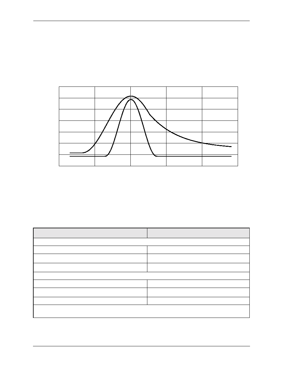
2.2.3.1 Transmit Pulse
Mask Templates
The Transmit Pulse Mask characteristics of the CX2833i device are designed so
that the transmitted output meets the Pulse Shape mask specified in ITU-T
Recommendation G.703.
Figure 2-4. Transmit Pulse Mask for DS3 Rates
Transmit Pulse Mask for DS3 Rates
-0.2
0
0.2
0.4
0.6
0.8
1
1.2
-1.
0
-0.
5
0.
0
0.
5
1.
0
1.
5
Normalized Symbol Time
N
o
r
m
a
lize
d
Pu
l
se
Amp
litu
d
e
NOTE(S): An Isolated Pulse is a pulse preceded by at least two zeros and followed by one or more zeros.
In judging the conformance of an isolated pulse to the mask, it is permissable to do the following:
1. Position the mask horizontally as necessary to encompass the pulse
2. Uniformly scale the amplitude of the isolated pulse to fit the mask
Table 2-1. DS3 Transmit Template Specifications
Time Axis Range (UI)
(1)
Normalized Amplitude Equation
Upper Curve
≠0.85
T
≠0.68
0.03
≠0.68
T
0.36
0.03 + 0.5 {1 + sin [(
/ 2)(1 + T / 0.34)]}
0.36
T
1.4
0.08 + 0.407 e
≠1.84(T ≠ 0.36)
Lower Curve
≠0.85
T
≠0.36
≠0.03
≠0.36
T
0.36
≠0.03 + 0.5{1 + sin[(
/ 2)(1 + T / 0.18)]}
0.36
T
1.4
≠0.03
NOTE(S):
(1)
UI = 1 / (System Clock Frequency)
2.0 Functional Description
CX28331/CX28332/CX28333 (-1x)
2.2 Transmitter
Single/Dual/Triple E3/DS3/STS-1 Line Interface Unit
2-6
Mindspeed Technologies
TM
28333-DSH-001-A
Mindspeed Proprietary and Confidential
Figure 2-5. Transmit Pulse Mask for STS-1 Rates
NOTE(S): An Isolated Pulse is a pulse preceded by at least two zeros and followed by one or more zeros.
In judging the conformance of an isolated pulse to the mask, it is permissable to do the following:
1. Position the mask horizontally as necessary to encompass the pulse
2. Uniformly scale the amplitude of the isolated pulse to fit the mask
Transmit Pulse Mask for STS-1 Rates
-0.2
0
0.2
0.4
0.6
0.8
1
1.2
-1.
0
-0.
5
0.
0
0.
5
1.
0
1.
5
Normalized Symbol Time
Norm
al
i
zed
P
ul
s
e
A
m
p
l
i
t
ude
Table 2-2. STS-1 Transmit Template Specifications
Time Axis Range (UI)
(1)
Normalized Amplitude Equation
Upper Curve
≠0.85
T
≠0.68
0.03
≠0.68
T
0.26
0.03 + 0.5 {1 + sin [(
/ 2)(1 + T / 0.34)]}
0.26
T
1.4
0.1 + 0.61 e
≠2.4(T ≠ 0.26)
Lower Curve
≠0.85
T
≠0.36
≠0.03
≠0.36
T
0.36
≠0.03 + 0.5 {1 + sin[(
/ 2)(1 + T / 0.18)]}
0.36
T
1.4
≠0.03
NOTE(S):
(1)
UI = 1 / (System Clock Frequency)

CX28331/CX28332/CX28333 (-1x)
2.0 Functional Description
Single/Dual/Triple E3/DS3/STS-1 Line Interface Unit
2.2 Transmitter
28333-DSH-001-A
Mindspeed Technologies
TM
2-7
Mindspeed Proprietary and Confidential
Figure 2-6. Transmit Pulse Mask for E3 Rate
500118a_1
17 ns
0.1
1.0
0.1
0.1
0.1
0.2
0.2
14.55 ns
8.65 ns
12.1 ns
24.5 ns
29.1 ns
Time
Volts
0.2
0.5
2.0 Functional Description
CX28331/CX28332/CX28333 (-1x)
2.2 Transmitter
Single/Dual/Triple E3/DS3/STS-1 Line Interface Unit
2-8
Mindspeed Technologies
TM
28333-DSH-001-A
Mindspeed Proprietary and Confidential
2.2.4 Alarm Indication Signal (AIS) Generator
When TAIS is asserted, an AIS replaces the transmit data at TPOS and TNEG.
The E3 type of AIS signal (all 1s) is supported. In three-level signal form, this is a
continuously alternating positive and negative pulse stream, as if the transmit data
were a continuous string of logical 1s.
Figure 2-7.
illustrates the AIS signal.
The TAIS pin has the same data latency as the TX data pins and can be used to
replace single symbols within a data stream. When the encoder is disabled
(ENDECDIS = 1), the TAIS mode maintains the proper phase, based upon the
polarity of the last 1 received.
The transmit AIS generator overwrites data during local loopback operation, it
does not affect remote loopback operation.
2.2.5 Jitter Generation (Intrinsic)
The CX2833i device meets the jitter generation requirements for various rates
with large margins, with the condition that the input transmit clock (TCLK) is
jitter-free. Data rates and jitter generation requirements are defined in the
following documents:
∑
E3 rate--ETSI TBR24, ITU-T G.823 (
Section 3.1.2
)
∑
DS3 rate--Bellcore GR499, AT&T Accunet TR54014, ITU-T G.824
∑
STS-1 rate--Bellcore GR253
Figure 2-7. AIS Signal
POSITIVE
PULSE
NEGATIVE
PULSE
TLINEP
(output voltage)
TLINEN
(output voltage)
8333_009

CX28331/CX28332/CX28333 (-1x)
2.0 Functional Description
Single/Dual/Triple E3/DS3/STS-1 Line Interface Unit
2.3 Receiver
28333-DSH-001-A
Mindspeed Technologies
TM
2-9
Mindspeed Proprietary and Confidential
2.3 Receiver
This section describes the detailed operation of the various blocks in the CX2833i
receiver.
2.3.1 Receive Sensitivity
The receiver recovers data from the coaxial cable that is attenuated due to the
frequency-dependent characteristics of the cable. In addition, the receiver
compensates for the flat loss (across all frequencies) in the various electrical
components and the variation in transmitted signal power.
The CX2833i device is able to recover data that has been attenuated by a
maximum of 900 feet of coax having characteristics and attenuation consistent
with ANSI T1.102-1993, Annex C, Figure C.2. This approximates the
characteristics of AT&T type 734/728 cable; almost the same attenuation
characteristic is achieved by one-half the length of AT&T type 735 cable.
2.3.2 AGC/VGA Block
The Variable Gain Amplifier (VGA) receives the AMI input signal from the
coaxial cable. The VGA supplies flat gain (independent of frequency) to make up
for various flat losses in the transmission channel and for loss at one-half the
symbol rate that cannot be made up by the equalizer. The VGA gain is controlled
by a feedback loop which senses the amplitude of the equalizer output, acting to
servo this amplitude for optimal slicing.
2.3.3 Receive Equalizer
The receive equalizer receives the differential signal from a VGA and boosts the
high frequency content of the signal to reduce intersymbol interference (ISI) to
the point that correct decisions can be made by the slicer with a minimum of jitter
in the recovered data.
The REQH pin when set high (REQH = 1) boosts the amount of equalization in
the receive side of the LIU. DS3/STS-1 pulses require a greater amount of
equalization then standard E3 pulses. REQH is therefore normally set high
(REQH = 1) for standard DS3/STS-1 pulses.
For cases where a square-shaped DS3/STS-1 pulse (that does not meet the
DS3/STS-1 standards) is transmitted to the receiver REQH can be set low (REQH
= 0).
In E3 mode, the REQH pin should always be set low (REQH = 0) to prevent
over-equalization.

2.0 Functional Description
CX28331/CX28332/CX28333 (-1x)
2.3 Receiver
Single/Dual/Triple E3/DS3/STS-1 Line Interface Unit
2-10
Mindspeed Technologies
TM
28333-DSH-001-A
Mindspeed Proprietary and Confidential
2.3.4 The PLL Clock Recovery Circuit
The clock recovery circuit (RX PLL) extracts the embedded clock from the sliced
data and provides this clock and the retimed data to the decoder (data mode).
Upon startup (after the internal reset is deasserted), the RX PLL uses a reference
clock (REFCLK) and a phase-frequency detector to lock to the correct data rate
(reference mode). During reference mode, the data outputs are squelched (set to
0). The RX PLL is kept in reference mode until a valid input is detected.
2.3.5 Loss Of Signal (LOS) Detector
The RLOS detector circuitry consists of two functional blocks: the analog section
and the digital. The analog section consists of high-speed, low-offset comparators
used for amplitude qualification. The digital block qualifies the pulse stream 1s
density and zero run length.
The digital block asserts RLOS when no valid pulses (per the analog section
described above) have been received for 128 REFCLKs. The digital block clears
the RLOS when the valid pulse density exceeds 20.3% with less than 64
consecutive zeros during an 128-symbol period.
2.3.6 B3ZS/HDB3 Decoder With Bipolar Violation Detector
In the CX2833i device, when ENDECDIS = 0 (encoder/decoder enabled), the
decoder takes the output from the clock recovery circuit and decodes the data
(HDB3 or B3ZS) into a single retimed NRZ data signal. The data signal is then
sent out of the CX2833i over the RNRZ (RPOS) pin. Any detected Line Code
Violations (LCV) are sent out over the corresponding RLCV (RNEG) pin. The
RLCV pin is asserted for one symbol period at the time the violation appears on
the RX output pin (RNRZ).
The following shows data sequence criteria for LCV; violations are indicated
in bold text. A valid bipolar pulse is indicated by a B. A bipolar violation
(non-alternating positive or negative) pulse is indicated by a V.
∑
Excessive zeros: 0, 0, 0, 0 (HDB3) or 0, 0, 0 (B3ZS). These violations are
passed on as 0 data on the RNRZ pin.
∑
Bipolar violation: B, 0, V (i.e., +1, 0, +1 or -1, 0, -1 for HDB3) B, V
(B3ZS and HDB3). These violations are passed on as 1 data on the RNRZ
pin.
∑
Coding violation: 0, 0, V (HDB3) or 0, V (B3ZS) with an even number of
Bs since the last valid 0 substitution V (follows coding rule). These
violations are passed on as 0 data on the RNRZ pin.
Table 2-3. RLOS Threshold Settings
Action
Min
(mV)
Typical
(mV)
Max
(mV)
RLOS Cleared
--
55
125
RLOS Declared
18
20
--

CX28331/CX28332/CX28333 (-1x)
2.0 Functional Description
Single/Dual/Triple E3/DS3/STS-1 Line Interface Unit
2.4 Jitter Tolerance
28333-DSH-001-A
Mindspeed Technologies
TM
2-11
Mindspeed Proprietary and Confidential
The even/odd counter (used to count the number of Bs between Vs) will count
a bipolar violation as a B. A coding violation or a valid 0 substitution resets the
counter.
When ENDECDIS = 1, the decoder is disabled, and the retimed slicer outputs
are sent out over RPOS (RNRZ) and RNEG (RLCV) pins. These outputs are then
decoded by the Framer or other downstream device. Line code violations are not
detected in this mode of operation. The decoder is configurable for either:
∑
E3 mode using HDB3 coding (E3MODE = 1)
∑
DS3/STS-1 mode using B3ZS coding (E3MODE = 0)
The receiver digital data outputs are centered on the rising edge of RCLK
(see
Section 2.9
).
2.3.7 Data Squelching
A counter in the receiver keeps track of the number of consecutive symbol
periods without a valid data pulse. When 128 or more 0s in a row are counted, the
receiver assumes that it has lost the signal and resets itself to try and regain the
signal. While the receiver is reacquiring the signal, the clock recovery block locks
to the reference clock and the data squelching is achieved by forcing the data bits
to zero. The data squelching is true in both NRZ and dual rail mode. When the
input signal has been properly amplified and equalized, the clock recovery PLL
will then switch to the incoming data.
2.4 Jitter Tolerance
The CX2833i receiver is able to tolerate a specified amount of high-frequency
jitter in the received signal while providing error-free operation (generally
defined as a bit error rate of less than 10
-9
). The specifications (illustrated in
Figure 2-9.
) for jitter tolerance are discussed in the following documents:
∑
E3 rate ≠ ITU-T G.823 and ETSI TBR24 contain frequency masks for input
jitter tolerance.
NOTE:
To meet jitter transfer requirements for loop-timed operation, an external
jitter attenuator is required. The jitter attenuator lessens jitter from the
receive clock.
∑
DS3 rate ≠ Bellcore GR499 specifies jitter tolerance frequency masks for
Category I and Category II interfaces.
∑
STS-1 rate ≠ Bellcore GR253 specifies a jitter tolerance. It is noted that the
STS-1 jitter tolerance differs from DS3 requirements only for Category II
interfaces.

2.0 Functional Description
CX28331/CX28332/CX28333 (-1x)
2.4 Jitter Tolerance
Single/Dual/Triple E3/DS3/STS-1 Line Interface Unit
2-12
Mindspeed Technologies
TM
28333-DSH-001-A
Mindspeed Proprietary and Confidential
Figure 2-8. Minimum Jitter Tolerance Requirement
Receiver Jitter Tolerance
1.0 UI
10 UI
0.1 UI
Jitter Frequency (Hz)
Input Jitter Amplitude
10 Hz
100 Hz
10 kHz
100 kHz
1 kHz
100604_014
1 MHz
2.3K
22.3K
60K
800K
300K
10
5
0.3
0.1
T3 [GR-499 (1995)]
Category II
T3 [GR-499 (1995)]
Category I
E3 [GR.823 (1993)]
1.5
0.15
Jitter Tolerance
CX28333

CX28331/CX28332/CX28333 (-1x)
2.0 Functional Description
Single/Dual/Triple E3/DS3/STS-1 Line Interface Unit
2.4 Jitter Tolerance
28333-DSH-001-A
Mindspeed Technologies
TM
2-13
Mindspeed Proprietary and Confidential
2.4.1 Jitter Transfer
The receiver must meet certain jitter transfer specifications between the input and
output jitter as a function of frequency. These specifications are only intended to
be met with the use of a jitter attenuator. Because the CX2833i does not contain a
jitter attenuator, one will have to be supplied externally. For reference purposes,
the specifications are discussed in the following documents and shown in
Figure
2-9.
E3 rate--Assume the same as DS3.
DS3 rate--Bellcore GR499, section 7.3.2 and Figures 7-3, 7-4, and 7-5,
defines and describes DS3 jitter transfer.
STS-1 rate--Bellcore GR253, section 5.6.2.1, defines and describes jitter
transfer for the STS-1 rate.
Figure 2-9. Maximum Jitter Transfer Curve Requirement
0.1 dB
Jitter Frequency
Jitter Gain
≠19.9 dB
STS-1 Category II
DS3 Category I
DS3 Category II
(Note: All slopes are 20 dB/decade)
10 Hz
100 Hz
1 kHz
10 kHz
100 kHz
100985_012

2.0 Functional Description
CX28331/CX28332/CX28333 (-1x)
2.5 Additional CX2833i Functions
Single/Dual/Triple E3/DS3/STS-1 Line Interface Unit
2-14
Mindspeed Technologies
TM
28333-DSH-001-A
Mindspeed Proprietary and Confidential
2.5 Additional CX2833i Functions
2.5.1 Bias Generator
To achieve good isolation between the channels, each channel utilizes an
independent power and ground to both transmit and receive. Additionally, each
channel has its own band gap voltage reference. Because only one external
resistor for current generation exists, only one band gap voltage can be used. The
band gap from Ch1 has been chosen for this task.
The 12.1 k
external resistor from pin RBIAS to ground, is specified to have
a tolerance of ±1%. This helps to keep tighter control on power dissipation and
circuit performance.
NOTE:
Capacitance should be kept to a minimum on the RBIAS pin.
2.5.2 Power-On Reset (POR)
If the system cannot guarantee a valid REFCLK frequency input during the POR
cycle, the CX2833i devices require assertion (active-high input pulse width, 1
µ
s
minimum) of the external reset signal (RESET, Pin 78 [80-pin package], Pin 97
[100-pin package]). Valid operation frequencies are DS3 (44.768 MHz
±
20
ppm), E3 (34.368 MHz
±
20 ppm), and STS-1 (51.84 MHz
±
20 ppm). Please
refer to the CX28331/2/3 Evaluation Module User Guide for crystal oscillator
specifications and vendor listings.
A POR circuit is provided in the CX2833i device to initialize all resettable
digital logic and analog control lines. The POR circuit uses a fixed RC timer
(~1
µ
s) to deassert itself when the power supply voltage reaches a minimum level
(~2 V). When the minimum supply voltage is reached (see
Table 2-6
), the
REFCLK input is counted for 128 clocks before the internal reset is deasserted.
At this time, the receiver block attempts to frequency lock (
±
5% tolerance) onto a
valid incoming REFCLK input. After frequency lock is achieved, the receiver
attempts to phase lock onto the valid RLINE receive signal.
NOTE:
If a valid REFCLK input is not present when POR releases the internal
reset, the receiver block may be unable to lock to the RLINE receive
signal. It is common for some crystal oscillator types oscillate at a lower
fundamental frequency if the crystal oscillator supply has not reached its
minimum operation voltage.
2.5.3 Loopback Multiplexers (MUXes)
Two loopback MUXes per channel in the CX2833i allow for local loopback
(terminal or framer side), remote loopback (cable side), or both. The RLOS signal
monitors the RX cable inputs irrespective of any loopback.
In remote loopback, set by asserting pin RLOOP high, the receive data
(retimed after clock recovery but not decoded) loops back into the pulse shaper in
place of the transmit data. Additionally, this data is sent out the RPOS, RNEG,
and RCLK pins.

CX28331/CX28332/CX28333 (-1x)
2.0 Functional Description
Single/Dual/Triple E3/DS3/STS-1 Line Interface Unit
2.5 Additional CX2833i Functions
28333-DSH-001-A
Mindspeed Technologies
TM
2-15
Mindspeed Proprietary and Confidential
In local loopback, set by asserting pin LLOOP, the transmit data loops back
immediately from the encoder output to the decoder input in place of the received
data. Additionally, this data is sent out the TLINEP and TLINEM/N pins.
Figures
2-10
and
2-11
illustrate remote and local loopback flow.
NOTE:
Transmit AIS operation overwrites data with an all 1's pattern during local
loopback, it does not affect remote loopback operation.
Figure 2-10. Remote Loopback Diagram
DECODER
PDATA
NDATA
DATCLK
P
N
ALOS
REQH
REFCLK
RLINEP
RLINEM/N
TLINEP
TLINEM/N
PDATA/
NDATA
TCLK
XOE
LBO
E3MODE
PDB
TPOS
TNEG
TCLK
TAIS
RLOOP
LLOOP
RPOS
RNEG
RCLK
RLOS
Pulse
Shaper
LINE
DRIVER
Encoder
E
NDE
CDIS
Clock/
Data
Recovery
Receiver
DATA
MUX
RLOSTHR
RLOSMAX
RLOSMDIS

2.0 Functional Description
CX28331/CX28332/CX28333 (-1x)
2.5 Additional CX2833i Functions
Single/Dual/Triple E3/DS3/STS-1 Line Interface Unit
2-16
Mindspeed Technologies
TM
28333-DSH-001-A
Mindspeed Proprietary and Confidential
Figure 2-11. Local Loopback Diagram
DECODER
PDATA
NDATA
DATCLK
P
N
ALOS
REQH
REFCLK
RLINEP
RLINEM/N
TLINEP
TLINEM/N
PDATA/
NDATA
TCLK
XOE
LBO
E3MODE
PDB
TPOS
TNEG
TAIS
RLOOP
LLOOP
RPOS
RNEG
RCLK
RLOS
Pulse
Shaper
LINE
DRIVER
Encoder
E
NDE
CDI
S
Clock/
Data
Recovery
Receiver
DATA
MUX
TCLK
RLOSTHR
RLOSMAX
RLOSMDIS

CX28331/CX28332/CX28333 (-1x)
2.0 Functional Description
Single/Dual/Triple E3/DS3/STS-1 Line Interface Unit
2.6 Mechanical Specifications
28333-DSH-001-A
Mindspeed Technologies
TM
2-17
Mindspeed Proprietary and Confidential
2.6 Mechanical Specifications
Figure 2-12. CX2833i-1x Mechanical Drawing (80-Pin)--Dimensions
D
3
D
3
D
D
1
D
1
D
2
D
D
1
D
2
A
L
A
1
L
1
A
2
Pin #1
Ref. Mark
e
b
See DETAIL B
TOP
DETAIL B
BOTTOM
c
Dim.
A
A1
A2
D
D1
D2
D3
L
L1
b
c
e
Coplanarity
0.05
0.95
15.75
13.90
0.45
0.09
1.20 MAX.
12.35 REF.
6.50 REF.
1.00 REF.
0.32 REF.
0.65 REF.
0.10 MAX.
0.15
1.05
16.25
14.10
0.75
0.20
0.002
0.040
0.620
0.547
0.018
0.004
0.047 MAX.
0.486 REF.
0.256 REF.
0.039 REF.
0.013 REF.
0.026 REF.
0.004 MAX.
0.006
0.041
0.640
0.555
0.030
0.008
Ref. 80-Pin ETQFP (GP00-D537)
Millimeters
Inches
Min.
Max.
Min.
Max.
100985_008

2.0 Functional Description
CX28331/CX28332/CX28333 (-1x)
2.7 Electrical Characteristics
Single/Dual/Triple E3/DS3/STS-1 Line Interface Unit
2-18
Mindspeed Technologies
TM
28333-DSH-001-A
Mindspeed Proprietary and Confidential
2.7 Electrical Characteristics
2.7.1 Absolute Maximum Ratings
Table 2-4. Absolute Maximum Ratings
Symbol
Parameter
Min
Max
Unit
DVDDC/
RVDD/
TVDD/
VDD/
VGG
Power Supply Voltage
≠0.3
6
V
V
I
Voltage on Any Signal Pin
≠1.0
VGG + 0.3 V
V
T
ST
Storage Temperature
≠40
125
∞C
T
VSOL
Vapor Phase Soldering
Temperature (1 min.)
--
220
∞C
JA
Thermal Resistance (Still
air, socketed)
--
40
∞
C
/
W
JA
Thermal Resistance (Still
air, soldered)
--
24
∞
C
/
W
Jc
--
--
7.40
∞
C
/
W
FIT
Failures in time @ 89,000
device hours, temperature
of 55 ∞C, 0 failures.
--
313
fits
NOTE(S):
1. Stresses above those listed as absolute maximum ratings may cause permanent damage
to the device. This is a stress rating only, and functional operation of the device at these or
any other conditions beyond those indicated in the other sections of this document is not
implied. Exposure to absolute maximum rating conditions for extended periods may affect
device reliability.

CX28331/CX28332/CX28333 (-1x)
2.0 Functional Description
Single/Dual/Triple E3/DS3/STS-1 Line Interface Unit
2.7 Electrical Characteristics
28333-DSH-001-A
Mindspeed Technologies
TM
2-19
Mindspeed Proprietary and Confidential
2.7.2 ESD Ratings
Testing Method--The devices were subjected to ESD events at the rated voltage
with both positive and negative polarities relative to each other pin or supply
domain on the device. The given pin was then curve-traced to detect leaky or
shorted ESD diodes. The criterion for passing is 3 devices that withstand voltage
without any leaky pins or functional failures.
2.7.3 Recommended Operating Conditions
Table 2-6
specifies various operating conditions, power supplies, and the bias
resistor.
Table 2-5. ESD Ratings
Model
Required Minimum
Observed
Human Body
1,000 V
2,000 V
Machine
100 V
200 V
Charged Device
400 V
700 V
Table 2-6. Recommended Operating Conditions
Parameter
Conditions
Min
Nom
Max
Unit
Power supply voltage
(
±
5%)
DVDDC, RVDD, TVDD,
VDD
3.135
3.3
3.465
V
ESD voltage
(1, 2)
VGG
3.135
5
5.5
V
External bias resistor
Pin RBIAS to GND; ±1%
11.98
12.1
12.22
k
NOTE(S):
(1)
With 5 V logic input, VGG should be tied to 5 V. With 3.3 V logic input, VGG should be tied
to 3.3 V. VGG must be equal or greater than power supply voltage.
(2)
When VGG is operated at 5V, sequence VGG to DVDDC, RVDD, TVDD, and VDD as
discussed in Appendix C.

2.0 Functional Description
CX28331/CX28332/CX28333 (-1x)
2.8 DC Characteristics
Single/Dual/Triple E3/DS3/STS-1 Line Interface Unit
2-20
Mindspeed Technologies
TM
28333-DSH-001-A
Mindspeed Proprietary and Confidential
2.8 DC Characteristics
Table 2-7. DC Characteristics
Parameter
Conditions
Min
Nom
Max
Unit
V
ih
high threshold
Digital inputs (Logic 1)
2.0
--
VGG + 0.3
V
V
il
low threshold
Digital inputs (Logic 0)
≠0.3
--
0.8
V
V
oh
high threshold
Digital outputs, I
oh
= ≠4 mA
2.4
--
--
V
V
ol
low threshold
Digital outputs, I
ol
= 4 mA
--
--
0.4
V
I
LEAK
(digital inputs and outputs)
0 V
digital Vin
VGG
≠10
--
200
µ
A
I
LEAK (analog inputs and outputs:
RLINExP, RLINExM,
TLINExP, TLINExM)
--
≠270
--
270
µA
Input capacitance
--
--
--
10
pF
Load capacitance
Digital outputs
--
--
15
pF
R
Line
/T
Line
capacitance
Maximum load
--
--
50
pF
Power Dissipation
Power dissipation CX28333
(≠1x)
Total chip
(3)
--
0.83
1.0
W
Power dissipation
(CX28332)
Total chip
--
--
0.8
W
Power dissipation
(CX28331)
Total chip
--
--
.450
W
NOTE(S):
1. The digital inputs of CX2833i are TTL 5 V compliant when VGG = 5V. These inputs are diode protected to the VGG pin.
Additionally, all of the CX2833i digital inputs contain 75 k
pull-down resistors.
2. The digital outputs of CX2833i are also TTL 5 V compliant when VGG = 5V. However, these outputs do not drive to 5 V, nor
do they accept 5 V external pull-ups.
3. Measured while transmitting and receiving all-1s pattern.

CX28331/CX28332/CX28333 (-1x)
2.0 Functional Description
Single/Dual/Triple E3/DS3/STS-1 Line Interface Unit
2.9 AC Characteristics
28333-DSH-001-A
Mindspeed Technologies
TM
2-21
Mindspeed Proprietary and Confidential
2.9 AC Characteristics
Table 2-8. AC Characteristics (Logic Timing)
Parameter
Conditions
Min
Nom
Max
Unit
Tosym, Tisym
RCLK and TCLK
E3 (34.368 MHz)
DS-3 (44.736 MHz)
STS-1 (51.84 MHz)
--
29.10
22.35
19.29
--
ns
ns
ns
Clock Duty Cycle
Towidth/Tosym, RCLK
Tiwidth/Tisym, TCLK
Tiwidth/Tisym, REFCLK
45
40
40
--
55
60
60
%
%
%
Todelay
--
--
--
3
ns
Tisetup
TPOS/TNRZ, TNEG,
TAIS
4
--
--
ns
Tihold
TPOS/TNRZ, TNEG,
TAIS
0
--
--
ns
NOTE(S):
1. The description applies to the DS3, E3, and STS-1 clock rates and other parameters such
as pulse width, set-up time, hold time, and duty cycle.
2. The timing diagram, illustrated in
Figure 2-13.
, describes the logical relationship
between various clock and data signals, and parameter values.
3. Todelay is measure with a 10≠15 pF loading characteristic.

2.0 Functional Description
CX28331/CX28332/CX28333 (-1x)
2.9 AC Characteristics
Single/Dual/Triple E3/DS3/STS-1 Line Interface Unit
2-22
Mindspeed Technologies
TM
28333-DSH-001-A
Mindspeed Proprietary and Confidential
Figure 2-13. Timing Diagram
TCLK
TPOS/TNRZ,
TNEG, TAIS,
Tisym
Tisetup
Tihold
DATA INPUTS
Don't
Care
Valid Data
Tiwidth
RCLK
RPOS/RNRZ,
RNEG/RLCV
Tosym
Todelay
DATA OUTPUTS
Towidth
Don't
Care
100604_016

28333-DSH-001-A
Mindspeed Technologies
TM
3-1
Mindspeed Proprietary and Confidential
3
3.0 Applications
The CX28331/CX28332/CX28333 can be used in a variety of applications.
Figure 3-1
illustrates an example of three DS3 lines being terminated by the
CX28333. The data and clock are extracted and passed on to the framer chip for
further data manipulation and user interface.
It is important to employ high-frequency design techniques for the printed
board layout.
3.1 PCB Design Considerations for the CX2833i
The CX28333 device is a mixed signal triple-port LIU device operating at
frequencies up to 51.84 MHz. This calls for a careful design of the PCB layout.
Some design considerations are outlined below.
3.1.1 Power Supply and Ground Plane
A single power plane with bulk capacitors (typically 10 µf) distributed throughout
the board will mitigate most power rail-related voltage transients. A bulk
capacitor should also be placed where the power enters the board. It is
recommended that decoupling capacitors be routed directly to each of the power
pins. It is recommended that 0.1 µf, 0.01 µf, and 0.001 µf decoupling capacitors
be used. All three values are not required on each pin, but values should be
dispersed uniformly to filter different frequencies of noise. 10 µf tantalum
capacitors should be placed on all four corners of the chip.
A continuous ground plane is the best way to minimize ground impedance. Most
ground noise is produced by the return currents and power supply transients
during switching. This effect is minimized by reducing the ground plane
impedance.
3.1.2 Component Placement
3.1.2.1 RBIAS Resistor
It is important to keep the RBAIS pins quiet, as any noise coupled to these pins
affect the internal references. The RBIAS resistors should be placed as close as
possible to the RBIAS pins and no digital signals should be routed near the pins
or the resistors. It is recommended to guard the pin, resistor, and traces with
ground vias.

3.0 Applications
CX28331/CX28332/CX28333 (-1x)
3.1 PCB Design Considerations for the CX2833i
Single/Dual/Triple E3/DS3/STS-1 Line Interface Unit
3-2
Mindspeed Technologies
TM
28333-DSH-001-A
Mindspeed Proprietary and Confidential
3.1.2.2 VGG Decoupling
It is recommended that the VGG pin be decoupled with a 0.1 µf, 0.01 µF and
0.001 µf capacitors. These capacitors should be placed close to the VGG pin.
3.1.2.3 Termination
Resistors and Capacitors
The termination resistors and capacitors on the receive RLINE pins should be
placed as close the receiver input on the chip as possible. The series resistors for
the transmit TLINE pins should also be placed as close to the transmitter output
pins as possible, but are less of a priority then the RLINE.
3.1.3 Impedance Matching
It is critical that both the transmit and receive traces around the transformers and
the matching resistors be kept to a minimum length and that the trace impedance
be matched to 75 ohms.
The transmit signals between the device and the transformer should be routed 75
ohm differentially. The transmit signals should be routed single ended between
the transformer and the BNC connector.
The receive signals should be routed differentially between the transformers and
either differentially or single ended from the transformers to the BNC connectors,
depending on the application. If the application requires ground termination it is
recommended that the signals be routed single ended. If the application does not
require ground termination, then the signals can be routed differentially.
To route signals differentially, the signal pair (positive and negative) should be 75
ohm coupled and should be surrounded by solid power/ground planes (buried
strip line) or be coupled to a power/ground plane (microstrip). Buried strip line is
recommended for internal layers while microstrip line is used for signals routed
on surface layers. There should be no discontinuity in the planes during the path
of the signal traces.
Single ended signals should be 75 ohm coupled between power/ground planes for
inner layers or 75 ohm coupled to a power/ground plane on the outer layers.
There should be no discontinuities in the power/ground planes over the trace path.
Impedance discontinuities occur when a signal passes through vias and travels
between layers. It is recommended to minimize the number of vias and layers
that the transmit/receive signals travel through in the design.
3.1.4 Other Passive Parts
Mindspeed recommends the use of 1:1 transformers for coupling the BNC
connectors to the device. The CX28333 uses six Pulse T3001 transformer devices
to handle the 3 Tx and 3 Rx channels.
It is recommended that a 220 µF tantalum capacitor be used where the power
enters the board.
3.1.5 IBIS Models
IBIS (Input/Output Buffer Interface Specification) models for the
CX28331/CX28332/CX28333-1x are available from Mindspeed's web site
(www.mindspeed.com).

CX28331/CX28332/CX28333 (-1x)
3.0 Applications
Single/Dual/Triple E3/DS3/STS-1 Line Interface Unit
3.1 PCB Design Considerations for the CX2833i
28333-DSH-001-A
Mindspeed Technologies
TM
3-3
Mindspeed Proprietary and Confidential
3.1.6 Recommended Vendors
Product: Transformers
Product: Crystals
America
Address:
Telo:
Fax:
Pulse
Corporate Office
12220 World Trade Drive
San Diego, CA 92128
858-674-8100
858-674-8262
Telo:
Fax:
E-mail:
Web site:
Crystek Corp.
12730 Commonwealth Drive
Fort Myers, FL 33913
800-237-3061
941-561-1025
sales@crystek.com
www.crystek.com
Northern Asia
Telo:
Pulse
3F-4, No. 81, Sec. 1
Hsin Tai Wu Road
Hsi-Chih
Tapei Hsien, Taiwan
R.O.C.
886-2-26980228
886-2-26980948
Northern Europe
Telo:
Fax:
Pulse
1S2 Huxley Road
The Surrey Research Park
Guildford, Surrey GU2 5RE
United Kingdom
44-1483-401700
44-1483-401701

3.0 Applications
CX28331/CX28332/CX28333 (-1x)
3.1 PCB Design Considerations for the CX2833i
Single/Dual/Triple E3/DS3/STS-1 Line Interface Unit
3-4
Mindspeed Technologies
TM
28333-DSH-001-A
Mindspeed Proprietary and Confidential
Figure 3-1. DS3/E3 Application Diagram
NOTE(S):
1. All transformers are part number T3001 from Pulse Technology. See Recommended Vendors,
Section 3.1.6
.
TX
TPOS
TNEG
TCLK
TLINEP
TLINEN
RX
RLINEP
RNEG
RLINEN
RPOS
RCLK
MODE
BIAS
RESET
Channel 1
CX28333
Framer
37.4
9
37.4
9
31.6
9
31.6
9
0.01µF
1:1
1:1
Type 728, 734, 735
75
9
Type 728, 734, 735
75
9
TX
TPOS
TNEG
TCLK
TLINEN
RX
RLINEP
RNEG
RLINEN
RPOS
RCLK
MODE
BIAS
RESET
Channel 2
TLINEP
TLINEP
Framer
37.4
9
37.4
9
31.6
9
31.6
9
0.01µF
1:1
1:1
Type 728, 734, 735
75
9
Type 728, 734, 735
75
9
TX
TPOS
TNEG
TCLK
TLINEN
RX
RLINEP
RNEG
RLINEN
RPOS
RCLK
MODE
BIAS
RESET
Channel 2
Framer
37.4
9
37.4
9
31.6
9
31.6
9
0.01µF
1:1
1:1
Type 728, 734, 735
75
9
Type 728, 734, 735
75
9
MODE
BIAS
RESET
RBIAS
12.1K
9
Mode/Status Pins
100985_009

28333-DSH-001-A
Mindspeed Technologies
TM
A-1
Mindspeed Proprietary and Confidential
A
Appendix A: Applicable Standards
The applicable standards documents are as follows:
∑
ANSI T1.102-1993 (DS3 and STS-1 standard)
∑
ANSI T1.404a-1996 (DS3 metallic interface)
∑
ITU Recommendation G.703 (DS3 and E3 standard)
∑
ITU Recommendation G.823 and G.824 (jitter and wander)
∑
Bellcore GR499, Issue 1, 12/89 (formerly TR-TSY-000499)
(DS3 and STS-1 requirements)
∑
Bellcore GR253, Issue 2, 12/91 (formerly TA-NWT-000253)
(STS-1 Requirements and Jitter)
∑
Bellcore TR-TSY-000191, Issue 1, 5/86 (AIS and LOS)
∑
ETSI TBR24 and TBR25 (E3 terminal equipment interface)
∑
ETSI ETS 300 686 and ETS 300 687 (E3 standard)
∑
AT&T Technical Reference TR54014, May 1992 (Accunet Interface
Specification for DS-3 jitter only)
∑
ETSI ETS 300 687, 1996, "Business Telecommunications; 34 Mbps Digital
Leased Lines (D34U and D34S); Connection Characteristics"
∑
ETSI ETS 300 686, 1996, "Business Telecommunication; 34 Mbps and 140
Mbps digital Leased Lines (D34U, D34S, D140U, and D140S); Network
Interface presentation"
∑
ANSI T1.102-1993, "Digital Hierarchy--Electrical Interfaces"
∑
ANSI T1.107-1995, "Digital Hierarchy--Formats Specification"
∑
ANSI T1.231-1997, Draft, "Digital Hierarchy--Layer 1 In-Service Digital
Transmission Performance Monitoring"
∑
ANSI T1.231-1993, "Digital Hierarchy--Layer 1 In-Service Digital
Transmission Performance Monitoring"
∑
ANSI T1.404-1994, "Network-to-Customer Installation--DS3 Metallic
Interface Specification"
∑
Bellcore GR-499-CORE, Issue 1, December 1995, "Transport Systems
Generic Requirements (TSGR): Common Requirements"
∑
Bellcore GR-253-CORE, Issue 2, December 1995, "SONET Transport
Systems: Common Generic Criteria"
∑
ITU Recommendation G.703, 1991, "Physical/Electrical Characteristics of
Hierarchical Digital Interfaces"
∑
ITU Recommendation G.823, 1993, "The Control of Jitter and Wander
Within Digital Networks Which are Based on the 2,048 kbps Hierarchy"
∑
ITU Recommendation O.151, 1992, "Error Performance Measuring
Equipment Operating at the Primary Rate and Above"
∑
ETSI TBR 24, 1997, "Business Telecommunication; 34 Mbps Digital
Unstructured and Structured Lease Lines; Attachment Requirements for
Terminal Equipment Interface"

Appendix A: Applicable Standards
CX28331/CX28332/CX28333 (-1x)
Single/Dual/Triple E3/DS3/STS-1 Line Interface Unit
A-2
Mindspeed Technologies
TM
28333-DSH-001-A
Mindspeed Proprietary and Confidential

28333-DSH-001-A
Mindspeed Technologies
TM
B-1
Mindspeed Proprietary and Confidential
B
Appendix B: Exposed Thin Quad Flat
(ETQFP) Pack
NOTE:
Mindspeed recommends that the exposed paddle on the CX2833i-1x be
soldered to the ground side of the PCB for reasons described below. Do
not route PCB traces or vias under the exposed paddle area of the
CX2833i-1x device.
The Exposed Thin Quad Flat Pack (ETQFP) package provides greater design
flexibility and increased thermal efficiency, while using a standard size IC
package. The exposed pad improves performance by permitting higher clock
speeds, more compact systems, and a more aggressive design criteria. ETQFP
thermal performance is better than standard packages; however, to make
optimum use of the thermal efficiencies designed into the ETQFP, the PCB must
be designed with this package in mind. The following sections of this document
provide more information regarding the thermal performance and PCB design for
Mindspeed ETQFPs.

Appendix B: Exposed Thin Quad Flat (ETQFP) Pack
CX28331/CX28332/CX28333 (-1x)
B.1 Introduction
Single/Dual/Triple E3/DS3/STS-1 Line Interface Unit
B-2
Mindspeed Technologies
TM
28333-DSH-001-A
Mindspeed Proprietary and Confidential
B.1 Introduction
The ETQFP is implemented using a standard epoxy-resin package mold
compound. The integrated circuit die is attached to the lead-frame die pad with a
thermally conductive epoxy. The leadframe is designed with a deep downset of
the die attach pad so it will be exposed on the bottom surface of the package after
mold. This provides an extremely low thermal resistance between the IC junction
and the exterior of the surface.
The die pad's external surface can be attached to the PCB using standard
solder reflow techniques. This allows efficient attachment to the board, and
permits the board structure to be used as a heat sink for the IC. Using thermal
vias, the lead frame die pad can be attached to a ground plane or special heat sink
structure designed into the PCB.
Figure B-1
illustrates the schematic of the
package components.
Figure B-1. Schematic Representation of the Package Components
100998_030
Lead Frame
Lead Frame
Mold Compound
Die
Die Attach

CX28331/CX28332/CX28333 (-1x)
Appendix B: Exposed Thin Quad Flat (ETQFP) Pack
Single/Dual/Triple E3/DS3/STS-1 Line Interface Unit
B.2 Package Thermal Characterization
28333-DSH-001-A
Mindspeed Technologies
TM
B-3
Mindspeed Proprietary and Confidential
B.2 Package Thermal Characterization
B.2.1 Heat Removal Path
The internal heat removal path is designed to transfer heat from the top surface of
the die to the die pad and then directly to the Printed Circuit Board (PCB) through
a center solder pad. The PCB must have features designed to remove heat from
the package efficiently. At a minimum, there must be an area of solder-tinned
copper underneath the ETQFP, called a thermal land. Heat is transferred from the
thermal land to the environment through thermal vias designed within the PCB
structure.
B.2.2 Thermal Lands
A thermal land is required on the surface of the PCB directly under the body of
the exposed package. During normal surface mount reflow, the exposed pad on
the underside of the package will be soldered to this thermal land creating an
efficient thermal path. The size of the thermal path is as large as needed to
dissipate the required heat.
For double-sided PCBs having no internal layers, the surface layers must be
used to remove heat.
Figure B-2
illustrates a sample package detail, including the
required solder mask and thermal land pattern for an EQTFP. The designer may
consider external means of heat conduction, such as attaching the copper planes
to a convenient chassis member or other hardware convection.
Figure B-2. Package and PCB Land Configuration
PCB Center Pad = Body Size - 2.0 mm
Thermal Via x N,
0.33 mm Dia.
Via Dia. + 0.1 mm
Mask Opening, F sq.
A
Metalization Pattern
Comp Side
Solder Mask
Comp Side
B
C
D
E
100998_024

Appendix B: Exposed Thin Quad Flat (ETQFP) Pack
CX28331/CX28332/CX28333 (-1x)
B.2 Package Thermal Characterization
Single/Dual/Triple E3/DS3/STS-1 Line Interface Unit
B-4
Mindspeed Technologies
TM
28333-DSH-001-A
Mindspeed Proprietary and Confidential
An array of 0.33 mm diameter thermal vias plated with 1 oz. copper must be
placed on the pad and shorted to the PCB's ground plane. If the plating thickness
in the exposed region of the center pad is not sufficient to effectively plug the
barrel of the via when plated, use solder mask to cap the vias; the mask diameter
should have a dimension equal to the via diameter + 0.1 mm minimum. This
prevents the solder from wicking through the thermal via, potentially creating a
solder void in the region between the package bottom and the center pad on the
surface of the PCB.
Table B-1
lists the dimensions for the entire ETQFP package
family.
Table B-1. Dimensional Parameters (mm)
Package Type
A
B
C
D
E
F
N
(1)
48-lead
ETQFP
5.40 5.40 0.50 0.25 1.00
4.70
sq.
3
x
3;
9
80-lead ETQFP
14.40
14.40
0.65
0.35
1.00
6.50 sq.
7 x 7; 49
100-lead ETQFP
14.40
14.40
0.50
0.25
1.00
8.00 sq.
7 x 7; 49
NOTE(S):
(1)
N represents the total number of thermal vias to be placed evenly across the entire PCB center pad. In the case of the 48-lead
ETQFP, all thermal vias are located within the exposed region of the center pad.

CX28331/CX28332/CX28333 (-1x)
Appendix B: Exposed Thin Quad Flat (ETQFP) Pack
Single/Dual/Triple E3/DS3/STS-1 Line Interface Unit
B.2 Package Thermal Characterization
28333-DSH-001-A
Mindspeed Technologies
TM
B-5
Mindspeed Proprietary and Confidential
B.2.3 PCB Design
Thermal vias are the primary method of heat transfer from the PCB thermal land
to the internal copper planes or to other heat removal sinks. The number, size, and
construction of the vias is important in obtaining the best package thermal
performance and package/PCB assembly. Thermal performance analysis
indicates there is a point of diminishing returns where additional vias will not
improve heat transfer through the board.
The PCB internal structure plays a very important role in package thermal
performance.
Figures B-3
and
B-4
illustrate the PCB structure for a two- and
six-layer design, respectively. PCB designs with more than two layers should
have all thermal vias connected to the ground plane.
Figure B-3. Internal Structure for a Two-Layer PCB
100998_029
1/2 Oz Copper Layer
60 Micron Solder Mask Layer
60 Micron Solder Mask Layer
1.50 mm
Core Laminate Layer
Thermal Via
1/2 Oz Copper Layer
Figure B-4. Internal Structure For a Six-Layer PCB
Core Laminate Layer
Thermal Via
Electrical Isolation
100998_028
1/2 Oz Copper Layer
60 Micron Solder Mask Layer
60 Micron Solder Mask Layer
1 Oz Copper Layer
1 Oz Copper Layer
1.50 mm
1 Oz Copper Layer
1 Oz Copper Layer
1/2 Oz Copper Layer

Appendix B: Exposed Thin Quad Flat (ETQFP) Pack
CX28331/CX28332/CX28333 (-1x)
B.2 Package Thermal Characterization
Single/Dual/Triple E3/DS3/STS-1 Line Interface Unit
B-6
Mindspeed Technologies
TM
28333-DSH-001-A
Mindspeed Proprietary and Confidential
B.2.4 Thermal Test Structure
B.2.4.1 Test
Environment
Package thermal performance has been tested following JEDEC standards. The
ETQFP package is mounted at the center of a 100 mm ◊ 100 mm, six layer test
board and is tested under different air flow velocities.
Figure B-5
illustrates the
system configuration.
B.2.4.2 Thermal Test
Boards
Two different test boards have been used to evaluate package thermal
performance for both worst and best conditions.
Table B-2
lists specifications of
these test boards.
Figure B-5. Test Performance Structure (A = 100 mm, B = 100 mm, L
P
= 1.40 mm, L
B
= 1.60 mm)
100998_027a
Air Flow
A
B
L
B
L
P
Table B-2. Specification for a Two-Layer Test Board
Drawing Number TR03-T1
Substrate Material
FR-4
Thickness 1.6
mm
Stackup (signal layers, Cu planes)
1S0P
Cu Coverage (signal layer--top/bottom) 10%
Cu Coverage (power/ground layer)
100%
Inner Cu Thickness (spec)
35
x
3.5
Table B-3. Specification for a Four-Layer Test Board
Drawing Number TR03-T2
Substrate Material
FR-4
Thickness 1.6
mm
Stackup (signal layers, Cu planes)
1S2P
Cu Coverage (signal layer--top/bottom) 10%
Cu Coverage (power/ground layer)
100%
Inner Cu Thickness (spec)
35
x
3.5

CX28331/CX28332/CX28333 (-1x)
Appendix B: Exposed Thin Quad Flat (ETQFP) Pack
Single/Dual/Triple E3/DS3/STS-1 Line Interface Unit
B.2 Package Thermal Characterization
28333-DSH-001-A
Mindspeed Technologies
TM
B-7
Mindspeed Proprietary and Confidential
B.2.5 Package Thermal Performance
B.2.5.1 Calculation
Guidelines
Maximum junction temperature can be calculated as:
T
j
= P x
ja
+ T
a
Where:
ja
= Equivalent Package Thermal Resistance (C/W)
T
j
= Maximum Junction Temperature (C)
T
a
= Ambient Temperature (C)
P
= Package Total Power Dissipation Value (W)
B.2.5.2 Package
Thermal Resistance
Delco thermal test chips are used to estimate package thermal performance.
Table B-4
lists thermal die specifications.
Figure B-6
illustrates package thermal resistance as a function of airflow velocity
for a 48-pin ETQFP package using two different test boards, specified in
Tables B-2
and
B-3
, and a prediction for a six-layer PCB design.
Figures B-7
and
B-8
illustrates the similar information for a 64- and 80-pin ETQFP package.
Table B-5
lists the test condition for each package type.
Table B-4. Specification for Delco Thermal Test Chips
Dimensions
3.81 mm x 3.81 mm
6.35 mm x 6.35 mm
7.8 mm x 7.8 mm
Thickness
0.33 mm
0.45 mm
0.5 mm
Figure B-6. Package Thermal Resistance as a Function of Airflow Velocity for a 48-ETQFP Package
0
10
20
30
40
50
60
70
80
0
50
100
150
200
250
300
350
400
450
500
Air Flow Velocity (LFM)
Package Thermal Resistance
Two Layer PCB
Four Layer PCB
Six Layer PCB
100998_031
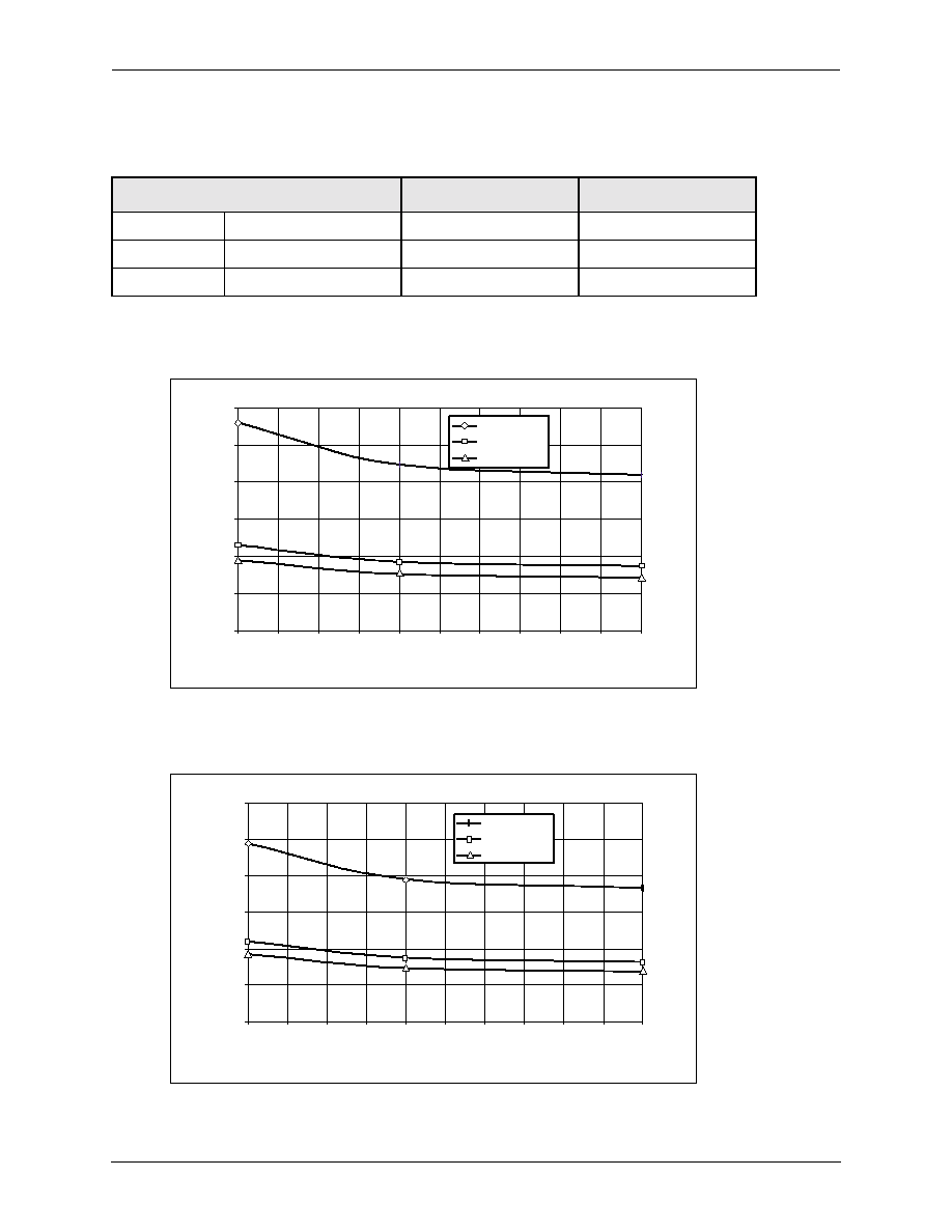
Appendix B: Exposed Thin Quad Flat (ETQFP) Pack
CX28331/CX28332/CX28333 (-1x)
B.2 Package Thermal Characterization
Single/Dual/Triple E3/DS3/STS-1 Line Interface Unit
B-8
Mindspeed Technologies
TM
28333-DSH-001-A
Mindspeed Proprietary and Confidential
Table B-5
lists the test conditions for
Figures B-6
through
B-8
.
Table B-5. Test Conditions
Package Type:
48 EQTFP
64 ETQFP
80 ETQFP
Body Size
7 mm x 7 mm
10 mm x 10 mm
14 mm x 14 mm
Die Size
3.81 mm x 3.81 mm
6.35 mm x 6.35 mm
7.8 mm x 7.8 mm
Die Pad Size
5 mm x 5 mm
7.50 mm x 7.50 mm
9.50 mm x 9.50 mm
Figure B-7. Package Thermal Resistance as a Function of Airflow Velocity for an 64 ETQFP
0
10
20
30
40
50
60
0
50
100
150
200
250
300
350
400
450
500
Air Flow Velocity (LFM)
Package Thermal Resistance
Two Layer PCB
Four Layer PCB
Six Layer PCB
100998_032
Figure B-8. Package Thermal Resistance as a Function of Airflow Velocity for an 80 ETQFP
0
10
20
30
40
50
60
0
50
100
150
200
250
300
350
400
450
500
Air Flow Velocity (LFM)
Package Thermal Resistance
Two Layer PCB
Four Layer PCB
Six Layer PCB
100998_033

CX28331/CX28332/CX28333 (-1x)
Appendix B: Exposed Thin Quad Flat (ETQFP) Pack
Single/Dual/Triple E3/DS3/STS-1 Line Interface Unit
B.3 Solder Stencil Determination
28333-DSH-001-A
Mindspeed Technologies
TM
B-9
Mindspeed Proprietary and Confidential
B.3 Solder Stencil Determination
Use the thickest possible solder mask, consistent with the components being
assembled to the PWB surface mount process. A standoff height of 2.0≠4.2 mils
provides good solder joints for both the leads and the center pad. This is achieved
using a stencil thickness of 5, 6, or 7 mils.
B.4 Solder Reflow Profile
The ETQFP uses the standard TQFP reflow profile because the ETQFP package
construction does not add thermal mass. There is minimal additional thermal load
due to the increased solder area between the exposed die pad on the package and
the center pad on the PCB.
Figures B-9
and
B-10
illustrate typical IR reflow
profiles for Sn63:Pb37 solder in the cases of natural convection and forced
convection ovens.

Appendix B: Exposed Thin Quad Flat (ETQFP) Pack
CX28331/CX28332/CX28333 (-1x)
B.4 Solder Reflow Profile
Single/Dual/Triple E3/DS3/STS-1 Line Interface Unit
B-10
Mindspeed Technologies
TM
28333-DSH-001-A
Mindspeed Proprietary and Confidential
Figure B-9. Typical IR Reflow Profile for Eutectic Sn63:Pb37
100998_025
NOTE(S):
Peak temperature should be approximately 220 ∞C, and the exposure time should normally be less
than 1.0 minutes at temperature above 183 ∞C.
300
270
240
210
180
150
120
90
60
30
0
Temperature
(∞
C)
1
2
3
4
5
6
7
8
9
10
0.0
219
Peak:
Max Slope: ≠3.2
Seconds Over 183: 48
Time
Minute
0.6
1
160
9
265
2
125
10
260
3
115
4
110
ZONE SETPOINTS
5
190
6
190
8
190
7
160
1.2
1.9
2.5
3.1
3.7
4.4
Belt Speed = 38.00 inches/minute

CX28331/CX28332/CX28333 (-1x)
Appendix B: Exposed Thin Quad Flat (ETQFP) Pack
Single/Dual/Triple E3/DS3/STS-1 Line Interface Unit
B.4 Solder Reflow Profile
28333-DSH-001-A
Mindspeed Technologies
TM
B-11
Mindspeed Proprietary and Confidential
Peak temperature should be approximately 235
∞
C, and the exposure time should
normally be less than 1.2 minutes at temperature above 183
∞
C. Belt Speed = 30
inches/minute (top and bottom setting), FAN SPEED = 2500 RPM, NITROGEN
LEVEL = 1200 SCFH.
Figure B-10. Typical Forced Convection Reflow Profile for Eutectic Sn63:Pb37
2470
1700
920
150
100998_026
File = SMOLE42
TWO2 - D675-001
MAXIMA
X
1= 221
2 = 225
3 = 227
4 = 226
Deg.
236.7
236.1
232.3
233.3
MAX SLOPES
X
1= 27
2 = 33
3 = 31
4 = 32
5 = 0
Deg./Point
4.4
6.7
6.7
9.4
0.0
Thermocouple Location
1 = BOTTOM GROUND
2 = TQFP4B
3 = BBA
4 = MCM
F1≠F4 = Sample 1≠4;
Temp
35.0
36.7
32.8
33.9
OPEN
F5 - ReScale X:
Slope
1.1
1.1
1.1
1.1
0.0
SAMP 1 X = ?3
SAMP 2 X = 67
SAMP 3 X = 182
SAMP 4 X = 244
Temp
147.2
157.8
153.9
160.0
OPEN
F6 - ReScale Y:
Slope
1.1
0.9
1.7
1.1
0.0
Temp
185.6
186.7
182.2
183.3
OPEN
F7 = PRINT:
Slope
1.1
1.7
1.7
1.1
0.0
Temp
185.0
181.1
187.8
182.2
OPEN
Msc = Menu:
Slope
≠2.2
≠4.4
≠2.8
≠3.3
0.0
+X----->
STATUS≠3
TEMP = 68
BATT = 5.893
P1s = 350
Act = X4321
00:00:01.0
04/29/98
12:00:08
ZONE 1 = 18
5
∞
C
ZONE 2 = 185
∞
C
ZONE 3 = 175
∞
C
ZONE 4 = 175
∞
C
ZONE 5 = 180
∞
C
ZONE 6 = 190
∞
C
ZONE 7 = 230
∞C
ZONE 8 = 270
∞
C

Appendix B: Exposed Thin Quad Flat (ETQFP) Pack
CX28331/CX28332/CX28333 (-1x)
B.4 Solder Reflow Profile
Single/Dual/Triple E3/DS3/STS-1 Line Interface Unit
B-12
Mindspeed Technologies
TM
28333-DSH-001-A
Mindspeed Proprietary and Confidential

28333-DSH-001-A
Mindspeed Technologies
TM
C-1
Mindspeed Proprietary and Confidential
C
Appendix C:
Power Sequencing
When VGG is operated at 5V, use the power-up and power-down sequencing
between VGG and VDD (DVDDC, RVDD, TVDD, VDD) as described in the
diagrams below (See note below).
NOTE:
VGG can exceed VDD by up to 5V (±10%) for short durations of less than 10 ms.
VGG must never be less than VDD by more than 0.5V.
Figure C-1. Power -up sequence of VGG and VDD.
VGGmax
VDD
VGGmin
VSS
3.6V Max.
3.6V Max.
0.5V Max.
0.5V Max.
3.6V Max.
Time
3.6V Max.
5.5V Max.
Figure C-2. Power-down sequence of VGG and VDD.
VGGmax
VDD
VGGmin
VSS
3.6V Max.
3.6V Max.
0.5V Max.
0.5V Max.
3.6V Max.
Time
3.6V Max.
5.5V Max.

Appendix C: Power Sequencing
CX28331/CX28332/CX28333 (-1x)
Single/Dual/Triple E3/DS3/STS-1 Line Interface Unit
C-2
Mindspeed Technologies
TM
28333-DSH-001-A
Mindspeed Proprietary and Confidential

www.mindspeed.com
General Information:
U.S. and Canada: (800) 854-8099
International: (949) 483-6996
Headquarters - Newport Beach
4311 Jamboree Rd. P.O. Box C
Newport Beach, CA. 92658-8902