
Rev.v6, 12 Apr 2002.
Information provided in this Data Sheet is subject to change without notice.
Pg. 1 of 14
Mindspeed
TM
Technologies, Inc.
Data Sheet
CX60083-15/-2A
10 Gbps High Gain Limiting Amplifier
Key Features
∑ Limiting amplifier
∑ Integrated LOS and peak detect circuit
∑ Wide bandwidth and high sensitivity
∑ Compatible with DC- or AC-coupled input and output signals
∑ Fully differential architecture
∑ Optional single-ended input and/or output operation
∑ Available in a 32-terminal, 5 mm square EdQuad TQFP or as dice
Applications
∑ Fiber-optic communications (OC-48/OC-192)
∑ SONET/SDH test equipment
∑ Data communications
Product Description
The CX60083 is a high-gain, wide-bandwidth, limiting amplifier ideal for use as a post-amplifier in fiber-optic receivers. With its 10GHz
bandwidth, this amplifier has been optimized for data rates up to 10.7 Gbps and has an input sensitivity (BER < 10
-10
) of 5 mV, differential. It
accepts both single-ended and differential inputs and may be either AC- or DC- coupled. With approximately 39 dB of small signal gain, this
amplifier can limit input voltages at or above 5 mV
P-P
(single-ended) to an output voltage of 460 mV
P-P
(single-ended).
An on-chip Loss of Signal (LOS) detection circuit with hysteresis provides an LOS output signal. A high-gain, on-chip, peak detector provides a
DC output signal that is linearly proportional to the input signal amplitude. This signal can be used for Automatic Gain Control (AGC) of preceding
amplifier stages or a custom LOS network. High-impedance differential outputs and inputs are available for input voltage offset correction.
The CX60083, as shown in Figure 7, is available in a 32-terminal flat pack or as shown in Figure 9 in die form. Figure 1 is the system block
diagram.
Figure 1. CX60083 System Block Diagram
OffInN
DatOutN
OffInP
Vth
VthCap
T I A
Supply
Voltage
OffOutP
OffOutN
PkDetOut
PkDetDC
LOSRes
LOS
AC or DC Coupled
Avalanche
Photodiode
Clock
Data
Recovery
Unit
DataInN
DataInP
CX60083
LOS
Detect
Peak
Detect
10k
DatOutP
See Figure 3 for
AC-Coupled
50
50
5
2k
2k
10k

CX60083-15/-2A, 10 Gbps High Gain Limiting Amplifier
Rev. v6, 12 Apr 2002.
Information provided in this Data Sheet is subject to change without notice.
Pg. 2 of 14
MindSpeed Technologies, Inc.
Signal Amplification and Termination
The CX60083 is optimized to accept up to 10.7 Gbps data on the 50
inputs DataInP and DataInN. The input signal is amplified 39 dB up to
approximately 460 mV
PP
(single-ended) and is limited to this value with any further input signal increase. Data rates greater than 10.7 Gbps
(including 12.5 Gbps) may be input but with reduced small signal gain.
The outputs are available at the DataOutP and DataOutN pins. The outputs have an internal 50
impedance and are designed to drive a 50
load. When terminated in 50
, the outputs swing between approximately ≠50 mV and approximately ≠510 mV.
The DataInP and DataInN inputs can be driven either differentially or single-ended, and can be DC-coupled or AC-coupled. Each of the
differential inputs has a 50
resistor terminated to the Vth terminal. In most cases Vth is grounded. However, it may be necessary to connect
Vth to a DC potential to ensure the input signal does not exceed the maximum or minimum CX60083 peak input voltage. These requirements are
described in more detail in Figure 4 and in the application note CX60083AN1: Input and Output Interface Terminations. VthCap provides for
additional (optional) decoupling of Vth.
Table 1 lists the CX60083 terminal name descriptions.
Table 1. Terminal Name Descriptions
Terminal Name
Terminal Number
Description
Signal
VthCap 2
Vth
Decoupling
DC
DataInP
4
High-speed Input Data (non-inverting polarity)
RF
(1)
DataInN
5
High-speed Input Data (inverting polarity)
RF
(1)
Vth
7
DataIn termination (Input Common Mode Voltage input when AC-coupled)
Power
OffInN
10
Negative Offset Control Input
Analog
OffInP
11
Positive Offset Control Input
Analog
OffOutP
15
Offset Sense Output (non-inverting)
Analog
OffOutN
16
Offset Sense Output (inverting)
Analog
DataOutN
20
High-speed Output Data (inverting polarity)
RF
(1)
DataOutP
21
High-speed Output Data (non-inverting polarity)
RF
(1)
PkDetDC
27
Peak Detector DC Reference
DC
PkDetOut
28
Peak Detector Output
DC
LOSRes
29
Loss Of Signal threshold control resistor
DC
LOS
30
Loss Of Signal (active high)
DC
Vee
1, 8, 17, 24, 25, 32
Power Supply
Power
Gnd
3, 6, 9, 12, 13, 14,
18, 19, 22, 23, 26, 31
Ground Power
EP
Exposed Paddle
Package or die backside
DC
(2)
Note 1: These are 50
matched terminals.
Note 2: The package or die backside should be well connected to ground using either conductive epoxy or solder.
Output Terminations
The outputs DataOutP and DataOutN can be either DC- or AC-coupled to the succeeding stage. For further details see Application Note
CX60083 AN1.
Offset Sense and Compensation
Differential output signals at DataOutP and DataOutN connect to pins OffOutP and OffOutN, respectively, via internal 10 k
resistors. These
pins can be used to reduce output offset that might produce pulse width distortion. The offset sense outputs indicate any DC offset voltage
between the differential outputs. They may be used in a feedback circuit to compensate for any internal voltage offset. The output of the offset
compensation circuit may be applied to one or both of the input offset compensation pins: OffInP and OffInN.
Output Signal Peak Detection
The on-chip peak detector generates a DC voltage on PkDetOut, which is proportional to the input signal amplitude. The PkDetDC output is the
DC reference voltage for the PkDetOut output signal. The difference between the PkDetOut and PkDetDC pins is a voltage, which is

CX60083-15/-2A, 10 Gbps High Gain Limiting Amplifier
Rev. v6, 12 Apr 2002.
Information provided in this Data Sheet is subject to change without notice.
Pg. 3 of 14
MindSpeed Technologies, Inc.
approximately linearly proportional to the input signal amplitude. The relationship of PkDetOut-PkDetDC, as a function of the input signal
amplitude, (differential, peak-to-peak) is illustrated in Figure 2.
Figure 2. Peak Detector Transfer Function Characteristics
PkDetOut - PkDetDC (mV)
0
200
400
600
800
1000
1200
0
20
40
60
80
100
120
140
160
180
Data Input Amplitude (mV
P-P
Differential)
mV DC
Loss of Signal
The LOS terminal is an open collector output providing an active high signal indicating a loss of signal (LOS) condition. The LOS terminal sinks
350
µA when it is low (deasserted) and no current when it is high (asserted). It is possible to connect the LOS terminal to a supply voltage using
an external resistor to establish a desired voltage logic level indicating LOS as described below.
The on-chip LOS circuit has built in hysteresis. To use the LOS function approximately 200
needs to be connected between the LOSRes pin
and ground.
LOS sinks 350
µA when it is low (deasserted), and no current when it is high (asserted). It is an active high output. You can connect a resistor
between 5 V or 3.3 V and the LOS pin. This can be used to establish output voltage levels as follows:
For a high level of 3.3 V and a low level of approximately 0.0 V, the swing is 3.3 V. When the output is low (not asserted) it sinks 350
µA. The
values: 3.3 V/350
µA is 9.4 k. Consequently, putting a 9.53 k resistor between 3.3 V and the LOS terminal would give you a 3.3 V output
when the signal is high and about 0.0 V when it is low.

CX60083-15/-2A, 10 Gbps High Gain Limiting Amplifier
Rev. v6, 12 Apr 2002.
Information provided in this Data Sheet is subject to change without notice.
Pg. 4 of 14
MindSpeed Technologies, Inc.
Figure 3. Loss of Signal (LOS) Characteristic
0
5
10
15
20
25
30
35
40
45
0
50
100
150
200
250
300
350
400
450
LOSRes ( )
I
nput
Si
gnal
(
m
Vpp,
si
ngl
e-
ended)
Vthreshold
(1)
Vhysteresis
(2)
Note 1: With the LOS flag reset, Vthreshold is defined as the input signal voltage, below which, the LOS flag becomes set.
Note 2: If LOS flag is set Vhysteresis is defined as the input signal voltage above which the LOS flag becomes reset.
Input Voltage Range Determination
The input AC voltage in combination with the DC bias present at the DataIn pins should satisfy the input voltage range specifications according to
the following condition: the voltage present at the input pins of the limiting amplifier (DataInP and/or DataInN) needs to fall between -1.0 V and
+0.25 V. From Figure 1 it can be observed that the differential voltage present at the CX60083 data inputs is a combination of the voltage at Vth
and the output level of the preamplifier driving the CX60083 data inputs.
Figures 4a and 4b show the relationship between the TIA output level and the Vth reference level to the voltage present at the CX60083 data
input pins when the input is either DC- (Figure 4a) or AC- (Figure 4b) coupled. (Note the TIA source level is Vs when terminated into a 50
load).
Figure 4a. CX60083 Input Value When DC-coupled
Ω TIA Driving Stage Output (Vs)
DataInP/N
Ω CX60083 Input
50
50
Transmission Line
Vth
DataInN/P =
±
±
±
± Vs
Vth
2
- 1.0 V
DataInN/P 0.25 V
50
0.1
µF
Vth Control
Voltage
Observe that if Vth = 0 V (ground), then the DataInP/N level is simply Vs.

CX60083-15/-2A, 10 Gbps High Gain Limiting Amplifier
Rev. v6, 12 Apr 2002.
Information provided in this Data Sheet is subject to change without notice.
Pg. 5 of 14
MindSpeed Technologies, Inc.
Figure 4b. CX60083 Input Value When AC-coupled
DataInP/N
Ω CX60083 Input
50
Transmission Line
DataInN/P = Vth
±
±
±
± Vs
50
- 1.0 V
DataInN/P 0.25 V
0.1
µF
Vth Control
Voltage
Ω TIA Driving Stage Output (Vs)
50
Vth Reference Value Determination
Referring to Figures 4a and 4b, for a preamplifier output signal of less than 250 mV
PEAK
, Vth can generally be connected to ground. If the input
signal is greater than 250 mV
PEAK
(and less than 800 mV
P-P
) then Vth will need to be connected to a negative voltage reference, the level of
which, is calculated so that the sum of the AC peak signal and the DC Vth reference voltage ensures the voltage present at DataInP and DataInN
input pins falls with the range -1.0 V and 0.25 V as shown in Figures 4a and 4b.
When driving the part with a single-ended input, the non-used CX60083 input terminal should be terminated in a manner similar to the input
being driven: if the driven input is DC-coupled to the preamplifier, the non-used input should be DC terminated with 50
. If the driven input is
AC-coupled, then the non-used input should be AC-coupled to the 50
termination. The termination voltage needs to be a potential equal to the
common mode voltage seen at the driven input terminal (so that the driving signal swings equally above and below the non-used input).
When a DC reference is connected to Vth, it should be decoupled with a good quality high frequency capacitor
10 nF (if possible, 0.1 µF in
parallel with 330 pF is suggested).
For more detailed information on interfacing to the CX60083 please refer to Application Note CX60083 AN1.

CX60083-15/-2A, 10 Gbps High Gain Limiting Amplifier
Rev. v6, 12 Apr 2002.
Information provided in this Data Sheet is subject to change without notice.
Pg. 6 of 14
MindSpeed Technologies, Inc.
Electrical Specifications
Tables 2 through 5 list the CX60083 RF and DC electrical specifications, absolute maximum ratings and power requirements.
Table 2. RF Electrical Specifications (for die, see Note 8)
Tcase = 0
∞C to +85 ∞C, Vee = ≠5.2 V ± 5%, Bit Rate = 9.95328 Gbps, input offset compensated for with DC servo loop and exposed paddle
connected to ground.
Parameter
Min
Typical
Max
Unit
Operating Temperature
0
--
85
∞C
Input AC Voltage, Single-ended
(1, 2)
5
--
800
mV
Input High Level (VIH) Voltage Range
(3)
≠1.0 -- 0.25
V
Input Low Level (VIL) Voltage Range
(3)
≠1.0 -- 0.25
V
Input Offset Voltage (without offset compensation)
(4)
≠5
0
5
mV
Output Swing, Single-ended (when limiting)
425
450
500
mV p-p
Absolute Output Voltage Range, Single-ended (when limiting)
≠0.6
--
0
V
Output Rise/Fall Time (20% - 80%), input = 20 mV p-p differential
(8)
--
28
35
ps
Small Signal Gain (single-ended to single-ended)
(5, 7)
32
39
--
dB
Small Signal Gain at 10 GHz (single-ended to single-ended)
(5, 7)
--
--
40
dB
Small Signal Gain Variation
(7)
≠2
0
+2
dB
Small Signal 3 dB Bandwidth
(7)
8.5
10.0
10.5
GHz
Input and Output Return Loss (single-ended) 100 kHz
- 5 GHz
(6, 7)
-- -- ≠10
dB
Input and Output Return Loss (single-ended) 5 GHz
- 10 GHz
(6, 7)
-- ≠10 ≠5
dB
Input and Output Return Loss (single-ended) 10 GHz
(6, 7)
-- ≠10 --
dB
Output Jitter (RMS), input = 1600 mV p-p differential
(8)
--
1.6
2.0
ps
Output Jitter (RMS), input = 10 mV p-p differential
(8)
--
2.1
3.0
ps
Note 1: 1600 mV differential peak-to-peak input translates to 800 mV
P-P
for each signal (single-ended). See Figure 5.
Note 2: Output typically limits for inputs greater than 5 mV
P-P
single-ended. Smaller and larger signals meeting the VIH and VIL specifications may be
input, but performance will be reduced.
Note 3: Signals exceeding 0.25V above ground but less than 0.5V above ground may be input, but performance will be reduced.
Note 4: End-of-life offset specification is
±
7 mV. For maximum sensitivity, a DC servo loop must be used (see Application Note CX60083 AN2).
Note 5: Unused input and output terminated 50
to ground. Differential to differential gain is 6 dB greater.
Note 6: Return Loss measured with packaged part mounted on a characterization board with 50
input and output traces and connectors.
Note 7: AC characteristics are established from characterization of packaged parts.
Note 8: While limited AC testing is done on each die, these characteristics are not guaranteed for die.
Figure 5. CX60083 Differential Input Voltage Definitions
DataInP
0.0
VID = [DataInP-DataInN]
1600 mV Max.
800 mV Max.
DataInN

CX60083-15/-2A, 10 Gbps High Gain Limiting Amplifier
Rev. v6, 12 Apr 2002.
Information provided in this Data Sheet is subject to change without notice.
Pg. 7 of 14
MindSpeed Technologies, Inc.
Table 3. DC Signal Electrical Specifications
Tcase = 0
∞C to +85 ∞C, Vee = ≠5.2 V ± 5%, Bit rate = 9.95328 Gbps
Parameter
Min
Typical
Max
Unit
PkDetOut ≠2.4
--
≠1.3
V
PkDetDC --
≠2.4
--
V
LOSOut
≠2.3
--
+6
(1)
V
LOSRes 50
--
500
LOS Assert/Deassert
250
ns
Note 1: Current sink output. Refer to the LOS subsection for description of voltage behavior.
Table 4. Absolute Maximum Ratings (no damage)
Symbol
Item
Min
Max
Units
Vee Supply
Voltage
≠7.0
+0.5
V
DataInP, DataInN
High Speed Input Signal
≠1.0
+0.5
V
DataOutP, DataOutN
High Speed Output Signal
≠1.0
+0.5
V
OffOutP, OffOutN
Offset Sense Output
≠2.0
+0.5
V
OffInP, OffInN
Offset Control Input
(1)
≠2.0
+2.0
V
Tst Storage
Temperature
≠65
+150
∞
C
Note 1: With Vth connected to ground
±
1 V, the offset control input range is
±
5 V.
Table 5. Power DC Electrical Specifications
Tcase = 0
∞C to +85 ∞C, Vee = ≠5.2 V ± 5%
Symbol
Item
Min
Typical
Max
Units
Iee Supply
Current
--
125
150
mA
Pdiss
Total Power Dissipation
--
650
825
mW

CX60083-15/-2A, 10 Gbps High Gain Limiting Amplifier
Rev. v6, 12 Apr 2002.
Information provided in this Data Sheet is subject to change without notice.
Pg. 8 of 14
MindSpeed Technologies, Inc.
CX60083 Applications Diagram
Figure 6. CX60083 Applications Diagram
Vee
Gnd
Gnd
Gnd
DataOutN
DataOutP
Gnd
Vee
Vee
Gn
d
LO
S
LO
S
R
es
Pk
D
e
t
O
u
t
Pk
D
e
t
D
C
Gn
d
Ve
e
Of
f
O
u
t
P
Of
f
O
u
t
N
Gn
d
Gn
d
Gn
d
Of
f
I
n
P
Of
f
I
n
N
Gn
d
CX60083
Vth
Gnd
Gnd
DataInN
DataInP
VthCap
+5V
14.3k
150
.01
1.0
.01
1.0
.01
.01 1.0
.01
.01
1.0
1.0
.01
.01
1.0
.01
.01
1.0
.01
24
22
21
23
20
19
18
17
16
15
14
13
12
11
10
9
25
26
27
28
29
30
31
32
1
3
4
2
5
6
7
8
+5V
2
3
7
4
6
U1
-
+
Vee
(-5.2V)
Optional ac
coupling.
Note 1.
Optional
single-ended
connection.
Note 2.
50
Optional ac
coupling.
Note 3.
Optional
single-ended
connection.
Note 3.
50
All Resistance values are in ohms
All Capacitance values are in mircofarads
Optional
Peak
Detect
Circuit
Vee
Vee
Notes:
1. The input(s) may be ac-coupled to the pre-amplifier using a good high frequency capacitor.
2. If driven single-ended by the pre-amplifier, the unused input must be terminated in 50 ohms.
If a single-ended ac-coupled connection to the preamplifier, the unused input must be ac-coupled
to a 50 ohm termination.
3. The output(s) may be ac-coupled to the CDR/receiver using a good high frequency capacitor.
4. If an output is connected single-ended to the receiver, the unused output must be terminated in 50 ohms.
If a single output is ac-coupled to the receiver, the unused output must be ac-coupled to a 50 ohm termination.
5. Package bottom must be attached to PCB ground using conductive epoxy or solder.
DC Servo (described in AN2)
Note 5
Optional
Loss of
Signal
Circuit
CX60083-15/-2A, 10 Gbps High Gain Limiting Amplifier
Rev. v6, 12 Apr 2002.
Information provided in this Data Sheet is subject to change without notice.
Pg. 9 of 14
MindSpeed Technologies, Inc.
CX60083 Package Pin Description
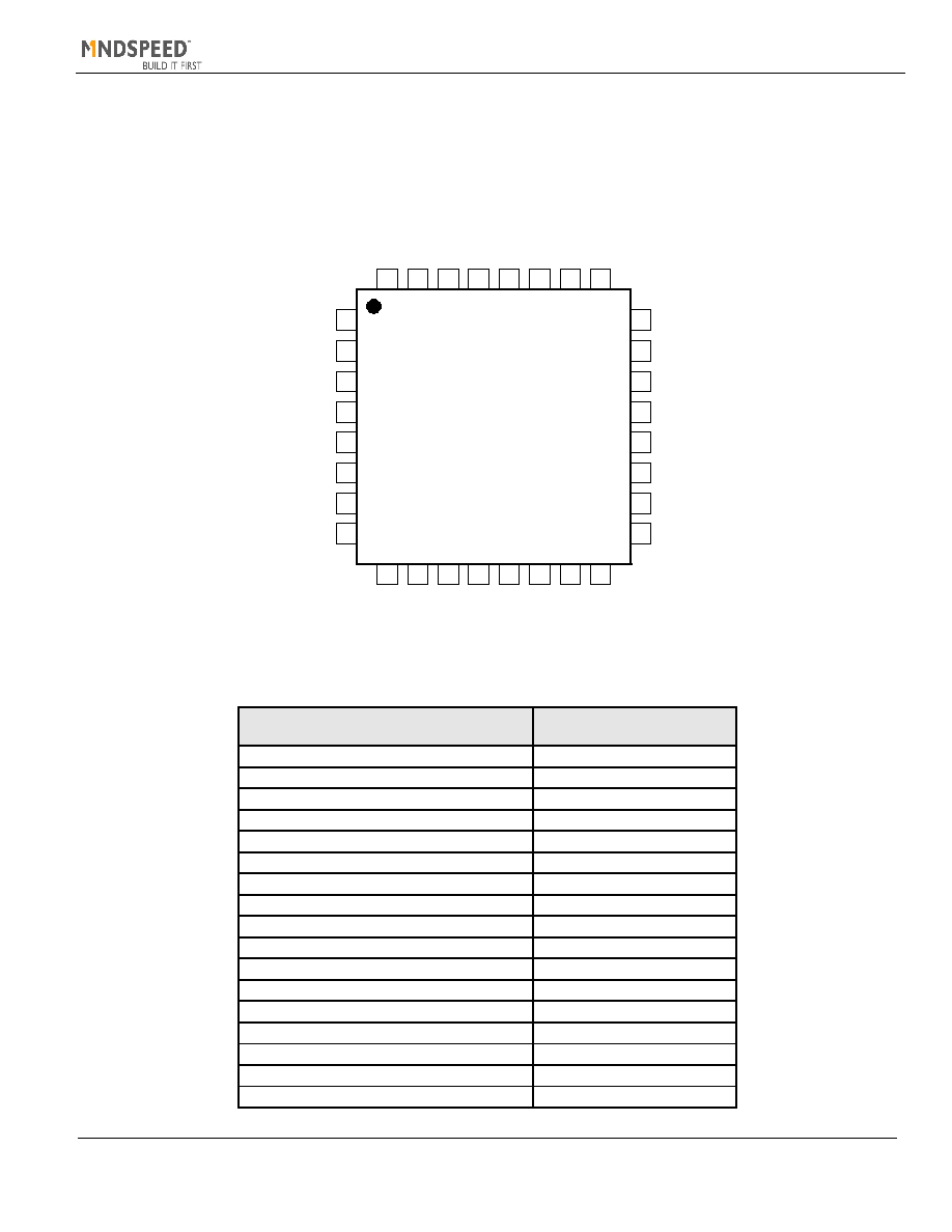
Figure 7 illustrates the pin number versus function configuration. Table 6 lists the pin assignments and function names. Figure 8 illustrates the
package pin dimensions.
Figure 7. CX60083 Pin Configuration (TQFP Package)
9
10
11
12
13
14
15
16
32
31
30
29
28
27
26
25
1
2
3
4
5
6
7
8
24
23
22
21
20
19
18
17
10G Post-Amp
CX60083
Vee
Vth
Vee
Gnd
Gnd
Gnd
DataInN
DataInP
VthCap
Vee
Gnd
Gnd
DataOutN
DataOutP
Gnd
Vee
TOP VIEW
O
ffO
utP
O
ffO
utN
Gn
d
Gn
d
Gn
d
O
ffInP
O
ffInN
Gn
d
V
ee
Gn
d
LO
SO
ut
LO
SRes
PkD
e
tOut
PkD
e
tDC
Gn
d
V
ee
Table 6. Package Pin Assignments
Package Pin
Signal
2 VthCap
4 DataInP
5 DataInN
7 Vth
10 OffInN
11 OffInP
15 OffOutP
16 OffOutN
20 DataOutN
21 DataOutP
27 PkDetDC
28 PkDetOut
29 LOSRes
30 LOS
1, 8, 17, 24, 25, 32
Vee
3, 6, 9, 12, 13, 14, 18, 19, 22, 23, 26, 31
Gnd
EP Gnd

CX60083-15/-2A, 10 Gbps High Gain Limiting Amplifier
Rev. v6, 12 Apr 2002.
Information provided in this Data Sheet is subject to change without notice.
Pg. 10 of 14
MindSpeed Technologies, Inc.
Figure 8. CX60083 Package Dimensions
Note: All dimensions are in millimeters.
BOTTOM VIEW
2.54 +/- 0.13 DIA.
EXPOSED HEATSINK
C 0.50 +/- .05 x 45 degree
TOP VIEW
PIN 1 ID.
0.50+/-0.05
D
D1
-D-
E1
E
-E-
-B-
SIDE VIEW
DETAIL X
R1
THETA 1
12 Degrees TYP.
R
GAGE PLANE
0.25
SEATING PLANE
L
THETA
e
Coplanarity
CCC - C -
-C-
A2 A
b
A1 (STANDOFF)
DETAIL X
CX60083-15/-2A, 10 Gbps High Gain Limiting Amplifier
Rev. v6, 12 Apr 2002.
Information provided in this Data Sheet is subject to change without notice.
Pg. 11 of 14
MindSpeed Technologies, Inc.
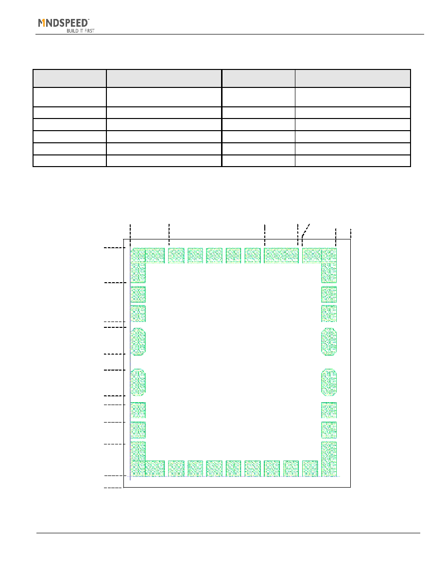
CX60083 Die Information and Pad Configuration Description
Table 7. Die Information
Item
Value
Item
Value
Product Availability
Die in Waffle Pack
Backside Bias
Most positive potential (0V) using
conductive epoxy
Process Technology
GaAs
Bond Pad Metalization
Au
Die Thickness
178 ± 13 µm
Pad pitch
150
µm
(1)
Die Size
1900
µm by 1750 µm
Pad size
120
µm X 120 µm
Die Passivation
Silicon nitride
Opening
93
µm X 93 µm
(2)
Die Backside Material
GaAs
Note 1: Others as indicated below.
Note 2: Other pad size indicated below.
Figure 9. CX60083 Die Pad Configuration Drawing
Gnd
Gnd
Gnd
Gnd
VthCap
Vth
DataInP
DataInN
Vee
DataOutP
243 µm
543 µm
805 µm
938 µm
243
µm
1200 µm
1118 µm
1350
µm
1593
µm
-78.5
µm
Vee
Gnd
Gnd
Gnd
Gnd
Gnd
Gnd
Vee
Vee
DataOutN
OffInN OffInP
OffOutP
N/C
OffOutN N/C
393 µm
625 µm
1500 µm
1743 µm
CX60083
LOS
Out
LOS
Res
PkDet
Out
PkDet
DC
-78.5 µm
0.0
0.0
543
µm
300
µm
Note: Pad sizes show exposed metal area only.

CX60083-15/-2A, 10 Gbps High Gain Limiting Amplifier
Rev. v6, 12 Apr 2002.
Information provided in this Data Sheet is subject to change without notice.
Pg. 12 of 14
MindSpeed Technologies, Inc.
Ordering Information
Name
Number
Package Data
10 Gbps Packaged Limiting Amplifier
CX60083-15
32-terminal EdQuad TQFP
10 Gbps Limiting Amplifier Die
CX60083-2A
Die in waffle pack
Revision History
Revision
Date
Comments
CLA10_rev1_2 10/13/99
CLA10
revisions
CX8610LA_rev1
1/20/00
Original CX8610LA issue
CX60083
2/1/00
Original CX60083 issue; added functional description text
CX60083v2a
2/18/00
Added illustrations and supporting text to functional description
CX60083v2b
2/10/00
Reorganized sequence of functional description and specification tables; added System Block Diagram
CX60083v2c
5/8/00
Transferred descriptive text from Note 2 in Table 3, RF Electrical Specifications to paragraph following table
CX60083v2d 5/12/00
Internal
document
CX60083v2e
6/19/00
Changed header and footer text; performed QA check and edits; edited Figure 1, System Block Diagram
CX60083v2f
8/8/00
Modified Table 1
CX60083v2g
9/15/00
Added Figure 3
CX60083v3 11/28/00
Technical
edits
CX60083v4 02/26/01
Technical
edits
CX60083v4a
03/12/01
Made CX60083≠15P from CX60083v4; added review comments; made changes to Figure 2, Table 2, and
Table 3 (return losses and bandwidth specifications)
CX60083v4b
05/4/01
Updated Table 2; became figure 2; updated figure and table references; added LOS assert/de-assert time
information; added offset specification note; added in die information; removed P designation; general edits
CX60083v5
01/23/02
Clarified jitter specification conditions. Update supply and output p-p numbers. Clarified input sensitivity
statements. Updated LOS current sink value. Made more explicit the proper connection of the package
bottom. Add applications diagram. Add die information and specifications
CX60083v5b
02/20/02
Added notes 3 and 7, modified note 2, moved other notes down. Added Table 7
CX60083v6
04/12/02
Corrected pin numbers on Applications Diagram (Fig. 6). Added ≠2A designator to header. Updated sales
office information.

CX60083-15/-2A, 10 Gbps High Gain Limiting Amplifier
Rev. v6, 12 Apr 2002.
Information provided in this Data Sheet is subject to change without notice.
Pg. 13 of 14
MindSpeed Technologies, Inc.
© 2002, Mindspeed Technologies, Inc.
All Rights Reserved.
Information in this document is provided in connection with MindspeedTM Technologies, Inc., as a wholly owned subsidiary and the Internet infrastructure
business of Conexant Systems, Inc., "Mindspeed" products. These materials are provided as a service to its customers and may be used for informational
purposes only. Mindspeed assumes no responsibility for errors or omissions in these materials. Mindspeed may make changes to specifications and product
descriptions at any time, without notice. Mindspeed makes no commitment to update the information and shall have no responsibility whatsoever for conflicts or
incompatibilities arising from future changes to its specifications and product descriptions.
No license, expressed or implied, by estoppel, or otherwise, to any intellectual property rights is granted by this document. Except as provided in Mindspeed
Terms and Conditions of Sale for such products, Mindspeed assumes no liability whatsoever.
THESE MATERIALS ARE PROVIDED "AS IS" WITHOUT WARRANTY OF ANY KIND, EITHER EXPRESSED OR IMPLIED, RELATING TO SALE AND/OR
USE OF MINDSPEED PRODUCTS INCLUDING LIABILITY OR WARRANTIES RELATING TO FITNESS FOR A PARTICULAR PURPOSE, CONSEQUENTIAL
OR INCIDENTAL DAMAGES, MERCHANTABILITY, OR INFRINGEMENT OF ANY PATENT, COPYRIGHT, OR OTHER INTELLECTUAL PROPERTY RIGHT.
MINDSPEED FURTHER DOES NOT WARRANT THE ACCURACY OR COMPLETENESS OF THE INFORMATION, TEXT, GRAPHICS OR OTHER ITEMS
CONTAINED WITHIN THESE MATERIALS. MINDSPEED SHALL NOT BE LIABLE FOR ANY SPECIAL, INDIRECT, INCIDENTAL, OR CONSEQUENTIAL
DAMAGES, INCLUDING WITHOUT LIMITATION, LOST REVENUES OR LOST PROFITS, WHICH MAY RESULT FROM THE USE OF THESE MATERIALS.
Mindspeed products are not intended for use in medical, life saving, or life sustaining applications. Mindspeed customers using or selling Mindspeed products for
use in such applications do so at their own risk and agree to fully indemnify Mindspeed for any damages resulting from such improper use or sale.
The following are trademarks of Mindspeed Technologies, Inc.: MindspeedTM, the symbol M1, and "Build It FirstTM". Product names or services listed in this
publication are for identification purposes only, and may be trademarks of third parties. Third-party brands and names are the property of their respective owners.
For additional disclaimer information, please consult Mindspeed's Legal Information posted at
http://www.mindspeed.com/
, which is incorporated by
reference.
Reader Response: Mindspeed strives to produce quality documentation and welcomes your feedback. Please send comments and suggestions to
tech.pubs@mindspeed.com
. For technical questions, contact your local Mindspeed sales office or field applications engineer.

CX60083-15/-2A, 10 Gbps High Gain Limiting Amplifier
Rev. v6, 12 Apr 2002.
Information provided in this Data Sheet is subject to change without notice.
Pg. 14 of 14
MindSpeed Technologies, Inc.
Further Information:
literature@mindspeed.com
(877) 908-5683 (United States)
(909) 975-5683 (International)
Headquarters
Mindspeed Technologies
4000 MacArthur Boulevard, East Tower
Newport Beach, CA 92660
Phone: (949) 579-3000
Fax: (949)
579-3020
Americas
US Northwest / Northwest Canada
Santa Clara
Phone: (408) 423-4500
Fax: (408)
249-7113
US North Central
Illinois
Phone: (630) 799-9300
Fax: (630)
799-9325
US South Central
Texas
Phone: (972) 735-1540
Fax: (972)
407-0639
Eastern Canada
Ontario
Phone: (613) 271-2358
Fax: (613)
271-2359
US Northeast
Massachusetts
Phone: (978) 244-7680
Fax: (978)
244-6868
US Southeast
North Carolina
Phone: (919) 858-9110
Fax: (919)
858-8669
US Florida / South America
Florida
Phone: (727) 799-8406
Fax: (727)
799-8306
US Mid-Atlantic
Pennsylvania
Phone: (215) 245-2470
Fax: (215)
245-2480
Europe
Europe Central - Germany
Austria, Germany, Hungary,
Poland, Romania, Russia and
Switzerland
Phone: (49) 89 82005 151
Fax: (49) 89 82005 150
Europe Mediterranean - Israel
Greece, Israel, Italy, Portugal and
Spain
Phone: (972) 9961-5100
Fax: (972) 9957 5166
Europe North - UK
Belgium, Denmark, Finland,
France, Ireland, Luxembourg,
Norway, Sweden, The Netherlands
and United Kingdom
Phone: 44 (0) 118 920 9500
Fax: 44 (0) 118 920 9595
Asia ≠ Pacific
P. R. China - Central and North
Australia and New Zealand
Phone: (86-21) 6350-5702
Fax: (86-21)-6361-2516
P. R. China - South / Hong Kong
Phone: 86-755-2300-420
Fax: 86-755-2300-421
Asia South - Taiwan
India, Indonesia, Malaysia,
Pakistan, Philippines, Singapore,
Taiwan, Thailand and Vietnam
Phone: (886-2) 8789-8366
Fax: (886-2)
8789-8367
Korea
Phone: 82-2-528-4301
Fax: 82-2-528-4305
Japan
Phone: (81-3) 5308 1731
Fax: (81-3)
5350-5431
http://www.mindspeed.com/