1/13
ML1001
ML1001 Series Static LCD COG Driver
v
Application
u Instrument LCD Module
u Telephone LCD Module
u Automotive LCD Module
u Handheld Device LCD Module
v
Features
l A Gold Bump Chip without external component.
l Logic & LCD power supply: 2.0V to 6.0V
l Typical Current consumption: 25uA at V
IN
= 3V
& no load condition.
l Number of segments: 40
l Cascade the ML1001 to form a single piece of 80
or 120 segments LCD driver.
l Simple 3 pin microcontroller interface through DIN, DCLK
& LOAD.
l Blink of the display data.
l Offer best contrast and widest viewing angle of TN LCD
technology.
l No temperature compensation needed for Topr = -40
o
C to
80
o
C.
ML1001 static LCD COG (chip on glass) driver is 40 segments LCD driver with gold bump. It can be
cascaded to form a single piece of 80 or 120 segments LCD drivers. It targets at custom TN LCD COG
Module product which requires the best quality of TN LCD technology. With the use of ML1001 series
driver, it offers the best contrast, the widest viewing angle, the widest range of operating voltage and the
widest range of operating temperature when compared to the multiplex method.
Our ML1001 includes an internal 32kHz oscillator, a 40-bit shift register, a 40-bit data register, a 16-bit
segment driver, a 24-bit segment driver, two common drivers, a blink control circuit, a power-up reset
circuit and a frequency divider which offer the necessary clock signals for Blink control, segment &
common driver circuit.
Through the DIN pin, the display data is serially shifted into the 40-bit shift register at the rising edge of
DCLK signal. The display data, which is going to be displayed on the attached LCD, is then stored in the
40-bit data register at the rising edge of the LOAD signal.
Other features like blinking of the display data by the BEN and BCLK, disable the internal oscillator by
the OEN, input an external clock signal to the FIN, and enable or disable the segment and common driver
by the SEN1, SEN2, CEN1A and CEN1B, are included.
v
General Description
v
Ordering Information
Part Number Description
Package Form
ML1001-1U a 40 segment static LCD driver Gold Bump Die
ML1001-2U a 80 segment static LCD driver Gold Bump Die
ML1001-3U a 120 segment static LCD driver Gold Bump Die

2/13
ML1001
v
Absolute Maximum Ratings
v
Block Diagram
Parameter
Symbol Condition
MIN
MAX
Unit
Supply voltage
V
DD
-0.5
+7.0
V
Supply Current
I
DD
V
DD
= 3V, no Load -50
+50
mA
Input Voltage
V
IN
GND-0.3 V
DD
+0.3 V
Output Voltage
V
OUT
GND-0.3 V
DD
+0.3 V
DC input Current
I
IN
-10
+10
mA
DC output Current
I
OUT
-10
+10
mA
Storage temperature
T
stg
-65
+150
o
C
Total power dissipation
P
tot
-
400
mW
DOUT
DIN
DCLK
LOAD
OEN
LCLK
S1
16-bit Segment Driver
S16
SEN1
24-bit Segment Driver
S17
S40
SEN2
Common Driver
COM1A
CEN1A
Common Driver
COM1B
CEN1B
40-bit Data Register
40-bit Shift Register
Blink Control
BEN
BCLK
Oscillator
Frequency Divider
FIN 2KHz 1KHz 500Hz 250Hz 125Hz 4Hz 2Hz 1Hz
OOUT
Power-Up Reset
3/13
ML1001
v
DC Characteristic
v
AC Characteristic
V
DD
= 3.0V; T
amb
= 25
o
C ; unless otherwise specified
Parameter
Symbol Condition
MIN
TYP
MAX
Unit
Supplies
Supply voltage
V
DD
2.0
-
6.0
V
Supply Current
I
DD
Disable Oscillator
-
0.1
0.5
uA
Supply Current
I
DD
Enable Oscillator
-
25
60
uA
Logic
LOW-level input voltage V
IL
GND
-
0.3*V
DD
V
HIGH-level input voltage V
IH
0.7*V
DD
-
V
DD
V
LOW-level output
current
I
OL
V
OL
= 1.0V
1
-
-
mA
HIGH-level output
current
I
OH
V
OH
= 2.0V
-1
-
-
mA
LCD outputs
Output resistance at pads
S1 to S40
R
SEG
-
85
150
ohm
Output resistance at pads
COM1A and COM1B
R
COM
-
45
100
ohm
V
DD
=3.0V; T
amb
= 25
o
C; unless otherwise specified
Parameter
Symbol Conditions
MIN
TYP
MAX
Unit
Oscillator frequency at
pad OOUT
f
oout
21
32
48
kHz
FIN, LOAD, DIN, DCLK
High time
t
H
0.4
-
-
us
FIN, LOAD, DIN, DCLK
Low time
t
L
0.4
-
-
us
FIN, LOAD, DIN, DCLK
Rise time
t
r
-
-
10
us
FIN, LOAD, DIN, DCLK
Fall time
t
f
-
-
10
us
DCLK Frequency
F
DCLK
1
-
1,000
kHz

4/13
ML1001
The ML1001 is a static LCD COG (chip on glass) driver which can drive upto 40 segments or cascaded
with two or three ML1001s to drive 80 & 120 segments. There is a shift register for serially shifting in the
data and a data register to store the data that is going to be displayed. The display data is read into the
shift register serially through the DIN pin at the rising edge of the DCLK signal. The display data will
then be displayed at the rising edge of the LOAD signal. The display data in the shift register is output by
the DOUT pin after 40 rising edges of the DCLK signal. The display data should be input in the sequence
of SEG40, SEG39... SEG2, SEG1 for proper display of data.
i) Power on reset
At Power on the ML1001 resets to a starting condition as follows:
1. The shift register outputs are set to GND.
2. The data register outputs are set to GND, hence all LCD segments off.
v
Timing Diagram
v
Functional Description
t
r
t
H
t
f
t
L
VIH
VIL
VIH
VIL
VIH
VIL
FIN, DIN,
DCLK, LOAD
1/F
DCLK
DIN
DCLK
40, 80 or 120 DCLKS
LOAD

5/13
ML1001
ii) Oscillator
a) Internal clock
The internal logic and the LCD driving signal of ML1001 are clocked either by the built-in oscillator or
from an external clock. When the internal oscillator is used, OEN should be connected to GND and the
OOUT should be connected to FIN. The oscillator will oscillate at 32 kHz and the frequency is
independent in the range of 2.0V < V
DD
< 6.0V
.
b) External clock
When using an external clock, the OEN is connected to VDD then connects the external clock to FIN.
iii) Timing
ML1001 have several frequencies of clock signal for the users to choose for the LCD display clock (ie.
LCLK) and the blink clock (ie. BCLK). They include the following clock signals :
Frequency of Clock Signal at FIN = 32 kHz Actual Divider of FIN Target Input Pin
2 KHz
1/16
1 KHz
1/32
500 Hz
1/64
256 Hz
1/128
128 Hz
1/256
LCLK
4 Hz
1/8192
2 Hz
1/16384
1 Hz
1/32768
BCLK
iv) Segment outputs
ML1001 has 40 segment outputs which should be connected directly to the LCD. If less than 40 segments
are required, the unused segments should be left open circuit. Users can disable the first 1 to 16 segments
and the last 17 to 40 segments by connecting the SEN1 and SEN2 to VDD, respectively. The segment
outputs shall output GND level after disabling it.
v) Common outputs
ML1001 consists of 2 common signals (ie. COM1A & COM1B). These two common signals are the
inversion of the LCLK. The common outputs should be left open-circuit if the outputs are unused. Users
can disable the COM1A and COM1B by connecting the CEN1A and CEN1B to VDD, respectively. The
common outputs will change to GND after disabling it.
vi) Blink
ML1001 has a blink function that users shall connect the BEN to GND and input the blink clock (ie.
BCLK) either by connecting ML1001 output clock signal from Frequency Divider or an external clock
signal. Users shall disable blink function by connecting BEN to VDD.

6/13
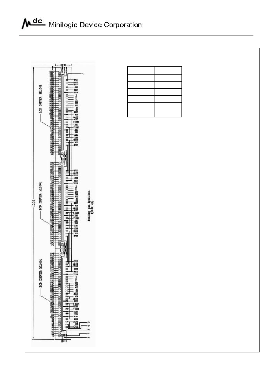
ML1001
Chip Size :
Part Number Description
Chip Size
ML1001-1U a 40 segment static LCD driver 3,440 um x 600 um
ML1001-2U a 80 segment static LCD driver 6,880 um x 600 um
ML1001-3U a 120 segment static LCD driver 10,320 um x 600 um
Chip Thickness : 400 um + 25 um
Gold Bump Pad Size : 32 um x 72 um
Gold Bump Height : 18 um + 2 um
Note :
1. The die faces up in the diagram.
v
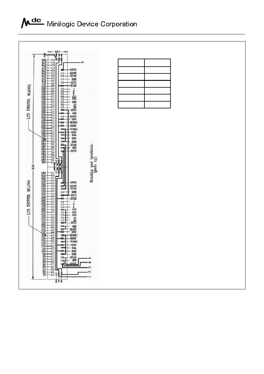
Pad Configuration
71 70 69
67
68
66 65 64 63 62
61
60
59 58 57 56 55 54 53 52 51 50 49 48 47 46 45 44 43 42 41 40 39 38 37 36 35 34 33 32
01 02 03 04 05
07
06
08 09 10 11 12 13 14 15 16 17 18 19 20 21 22 23 24 25
27 28
26
72
73
74
31
30
29
ML1001

7/13
ML1001
All x and y coordinates are references to the left lower corner of the chip.
v
Pad Location
PAD
PAD
PAD
PAD
PAD
PAD
Num.
Name
X
Y
Num.
Name
X
Y
Num.
Name
X
Y
1
LOAD
20
40
26
DCLK
2320
40
51
S21
1286
320
2
DIN
120
40
27
DOUT
2400
40
52
S20
1206
320
3
DCLK
220
40
28
LOAD
2500
40
53
S19
1126
320
4
BEN
320
40
29
GND
2826
60
54
S18
1046
320
5
OEN
420
40
30
VDD
2826
140
55
S17
966
320
6
VDD
520
40
31
COM1B
2826
220
56
S16
886
320
7
SEN1
600
40
32
S40
2806
320
57
S15
806
320
8
CEN1A
700
40
33
S39
2726
320
58
S14
726
320
9
SEN2
800
40
34
S38
2646
320
59
S13
646
320
10
CEN1B
900
40
35
S37
2566
320
60
S12
566
320
11
GND
1000
40
36
S36
2486
320
61
S11
486
320
12
OOUT
1080
40
37
S35
2406
320
62
S10
406
320
13
FIN
1180
40
38
S34
2326
320
63
S9
326
320
14
LCLK
1280
40
39
S33
2246
320
64
S8
246
320
15
2 KHz
1360
40
40
S32
2166
320
65
S7
166
320
16
1 KHz
1440
40
41
S31
2086
320
66
S6
86
320
17
500 Hz
1520
40
42
S30
2006
320
67
S5
6
320
18
250 Hz
1600
40
43
S29
1926
320
68
S4
-74
320
19
125 Hz
1680
40
44
S28
1846
320
69
S3
-154
320
20
4 Hz
1760
40
45
S27
1766
320
70
S2
-234
320
21
2 Hz
1840
40
46
S26
1686
320
71
S1
-314
320
22
1 Hz
1920
40
47
S25
1606
320
72
COM1A
-294
220
23
BCLK
2020
40
48
S24
1526
320
73
VDD
-294
140
24
LCLK
2120
40
49
S23
1446
320
74
GND
-294
60
25
BEN
2220
40
50
S22
1366
320
Coordinate
Coordinate
Coordinate
8/13
ML1001
Note :
1. In cascade format of ML1001(ie. ML1001-2U and �3U), one pin is the input of current ML1001 and
the other is for the connection with the corresponding input pin of next ML1001.
2. All Enable pins are active low.
3. Condition : FIN = 32 KHz Clock.
v
Pin Description
Symbol
Pad
Description
LOAD
1,28
Load data from the shift register to data register; note 1
DIN
2
Display data input pin
DCLK
3,26
Input pin for the clock of the display data; note 1
BEN
4,25
Enable pin of the blink function; note 1, note 2
OEN
5
Enable pin of the internal oscillator; note 2
V
DD
6
Supply voltage
SEN1
7
Enable pin of the segment from S1 to S16; note 1
CEN1A
8
Enable pin of the COM1A; note 2
SEN2
9
Enable pin of the segment from S17 to S40; note 1
CEN1B
10
Enable pin of the COM1B; note 2
GND
11
Logic ground
OOUT
12
Output pin of the internal oscillator
FIN
13
Input pin of the external/internal clock
LCLK
14,24
Input pin to the LCD display clock; note 1
2 kHz
15
Output 1/16 frequency of the input to the FIN; note 3
1 kHz
16
Output 1/32 frequency of the input to the FIN; note 3
512 Hz
17
Output 1/64 frequency of the input to the FIN; note 3
256 Hz
18
Output 1/128 frequency of the input to the FIN; note 3
128 Hz
19
Output 1/256 frequency of the input to the FIN; note 3
4 Hz
20
Output 1/8192 frequency of the input to the FIN; note 3
2 Hz
21
Output 1/16384 frequency of the input to the FIN; note 3
1 Hz
22
Output 1/32768 frequency of the input to the FIN; note 3
BCLK
23
Input pin for the blink clock
DOUT
27
Output pin for 40-bit Shift register, it shall connect to DIN of next ML1001
GND
29
Logic ground
V
DD
30
Supply voltage
COM1B 31
Common driving signal to LCD panel
S40 to S1 32 to 71 LCD segment outputs
COM1A 72
Common driving signal to LCD panel
V
DD
73
Supply voltage
GND
74
Logic ground
9/13
ML1001
Note : Pin LOAD and Pin CHECK shall be connected together if the flip-chip assembly is in good
condition. Hence, Pin CHECK can be served for qualifying the flip-chip assembly quality.
v
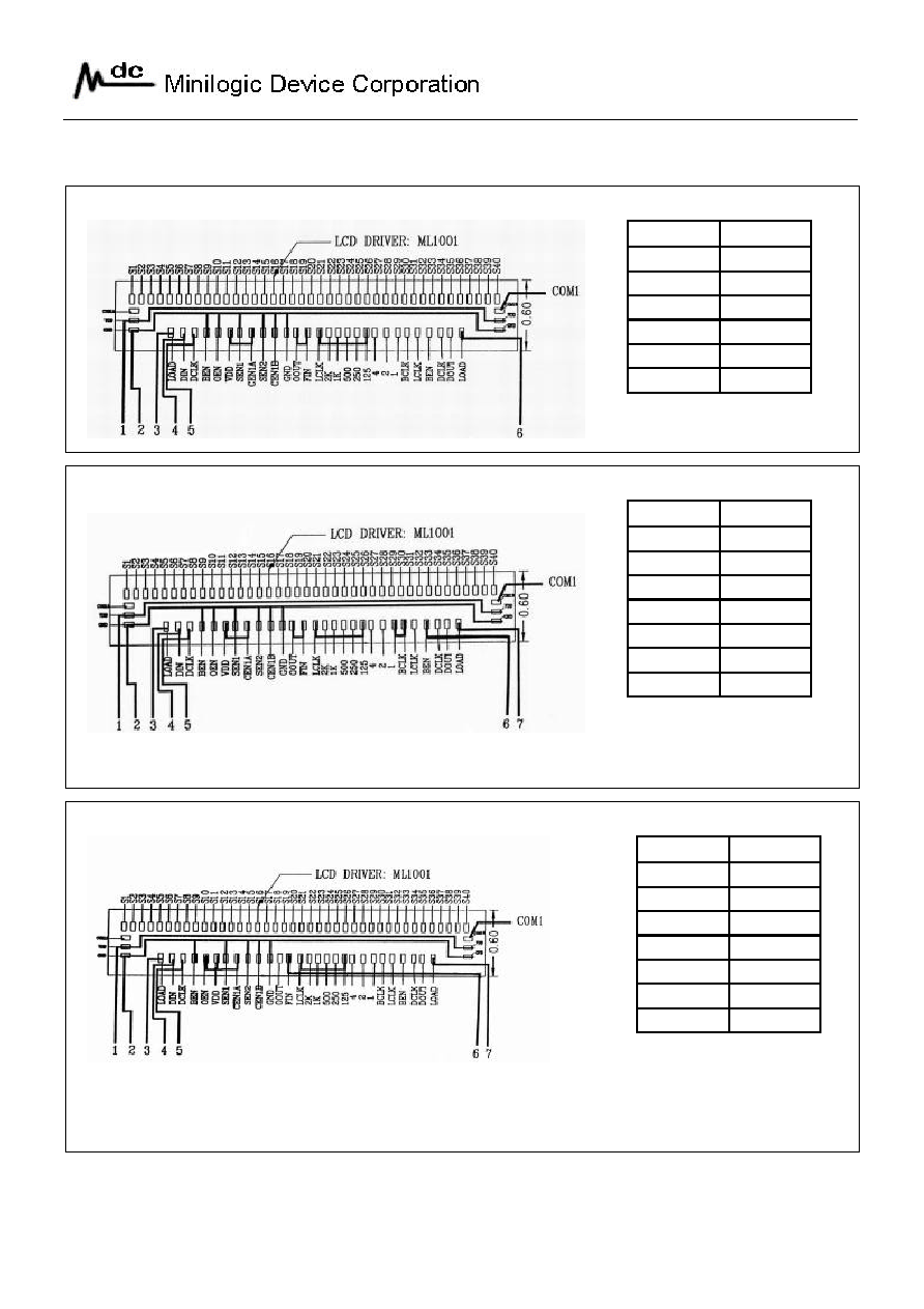
Application Examples
ML1001-1U Standard Application
Pin
Number
Pin Name
1
VDD
2
GND
3
LOAD
4
DIN
5
DCLK
6
CHECK
ML1001-1U Application Circuit with 1 Hz Blink Feature
Pin
Number
Pin Name
1
VDD
2
GND
3
LOAD
4
DIN
5
DCLK
6
BEN
7
CHECK
ML1001-1U Application Circuit with External 32 KHz Clock
Note : Blink at 1 Hz if BEN = 0V, Normal Display if BEN = VDD.
Pin
Number
Pin Name
1
VDD
2
GND
3
LOAD
4
DIN
5
DCLK
6
FIN
7
CHECK
Note : If External 32 KHz Clock Signal is available, designer can turn off Internal Oscillator
to save power.
10/13
ML1001
ML1001-2U Standard Application
Pin
Number
Pin Name
1
VDD
2
GND
3
LOAD
4
DIN
5
DCLK
6
CHECK
Note :
Chip 1 Pad Coordinate shall follow "Table of Pad Location".
Chip 2 Pad Coordinate shall be calculated as follow :
Chip 2 X-Coordinate = Chip 1 X-Coordinate + 3,440um
Chip 2 Y-Coordinate = Chip 1 Y-Coordinate
11/13
ML1001
ML1001-3U Standard Application
Pin
Number
Pin Name
1
VDD
2
GND
3
LOAD
4
DIN
5
DCLK
6
CHECK
Note :
Chip 1 Pad Coordinate shall follow "Table of Pad Location".
Chip 2 Pad Coordinate shall be calculated as follow :
Chip 2 X-Coordinate = Chip 1 X-Coordinate + 3,440um
Chip 2 Y-Coordinate = Chip 1 Y-Coordinate
Chip 3 Pad Coordinate shall be calculated as follow :
Chip 3 X-Coordinate = Chip 1 X-Coordinate + 6,880um
Chip 3 Y-Coordinate = Chip 1 Y-Coordinate

12/13
ML1001
Note: 1.
Contrast ratio of LCD shall vary from the Liquid Crystal used.
2. Contrast ratio of 1/3 Duty LCD is shown on graph 4 for comparison only.
3. The viewing angle is measured from the normal of LCD as shown below.
v
Typical Characteristics
1) Supply Current vs. Frequency of LCLK
2) Supply Current vs. Input Voltage
0
100
200
300
400
500
600
700
800
0
1
2
3
4
5
6
7
Input Voltage VIN(V)
Supply Current ISS(uA)
Load = 25nF
With Load
No Load
0
200
400
600
800
1000
1200
1400
1600
0
500
1000
1500
2000
2500
LCD Frequency LCLK(Hz)
Supply Current ISS(uA)
VDD = 2V
VDD = 3V
VDD = 4V
VDD = 5V
VDD = 6V
Load = 25nF
3) Example of Contrast Ratio vs. Input Voltage
0
2
4
6
8
10
12
0.0 V
1.0 V
2.0 V
3.0 V
4.0 V
5.0 V
6.0 V
Input Voltage VIN(V)
Contrast Ratio
4) Example of Contrast Ratio vs. Viewing Angle
0
2
4
6
8
10
12
0
10
20
30
40
50
60
70
80
Viewing Angle (degree)
Contrast Ratio
ML1001 Static TN COG Module
VIN = 3V
1/3 Duty LCD
0 degree
Observer
Viewing Angle
LCD

13/13
ML1001
REV
DESCRIPTION
DATE
First Official Specification
8/11/02
v
History of Revision
The information presented in this document does not form part of any quotation or contract, is believed to be accurate and
reliable and may be changed without notice. No liability will be accepted by the publisher for any consequence of its use.