ML61
ML61 Series Positive Voltage Detector
Application
Memory Battery Back-up Circuits
Microprocessor Reset Circuitry
Power Failure Detection
Power-on Reset Circuit
System Battery Life and Charge Voltage
Monitor
Features
CMOS Low Power Consumption : Typical 1.0uA at
Vin=2.0V
Selectable Detect Voltage : 1.1V to 6.0V in 0.1V increments
Highly Accurate : Detect Voltage 1.1V to 1.9V + 3%
Detect Voltage 2.0V to 6.0V + 2%
Operating Voltage : 0.8V to 10.0V
Package Available : SOT23 (150mW), SOT89 (500mW)
& TO92 (300mW)
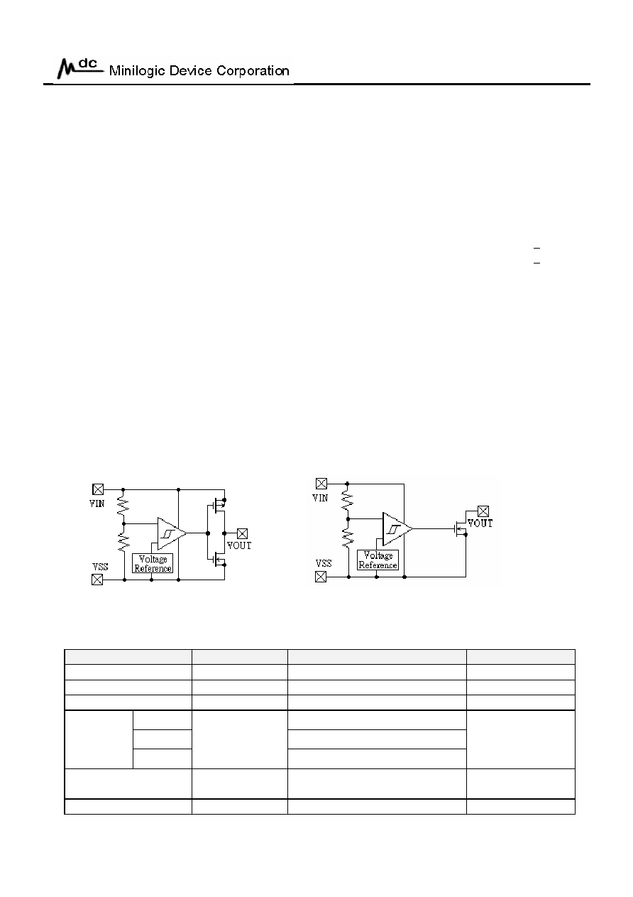
Block Diagram
(1)
CMOS
Output
(2)
N-Channel
Open
Drain
Output
General Description
The ML61 is a group of high-precision and low-power voltage detectors.
The ML61 consists of a highly-accurate and low-power reference voltage source, a comparator,
a hysteresis circuit, and an output driver. Detect voltage is very accurate and stable with
N-channel open drain and CMOS, are available.
Absolute Maximum Ratings
P1/14
Parameter
Symbol
Ratings
Units
Input Voltage
V
IN
10 V
Output Current
I
OUT
50 mA
Output Voltage
V
OUT
V
SS
-0.3 ~V
IN
+0.3 V
SOT-23 150
SOT-89 500
Continuous
Total Power
Dissipation
TO-92
P
d
300
mW
Operating Ambient
Temperature
T
opr
-40 ~ +70
o
C
Storage Temperature
T
stg
-40 ~ +70
o
C

ML61
Electrical Characteristics
Parameter
Symbol
Conditions
Min
Typ
Max Units
V
DF
= 1.1V to 1.9V
X0.97
V
DF
X1.03 V
Detect Voltage
V
DF
V
DF
= 2.0V to 6.0V
X0.98
V
DF
X1.02 V
Hysteresis Range
V
HYS
X0.02 V
DF
X0.05 X0.07 V
V
IN
= 1.0V
0.8
2.0
V
IN
= 2.0V
1.0
2.5
V
IN
= 3.0V
1.3
3.0
V
IN
= 4.0V
1.6
3.5
Supply Current
I
SS
V
IN
= 5.0V
2.0
4.0
uA
Operating Voltage
V
IN
V
DF
= 1.1~6.0V
0.8
10.0
V
Nch
V
DS
= 0.5V
V
IN
= 1.0V
1.0
V
IN
= 2.0V
3.0
V
IN
= 3.0V
5.0
V
IN
= 4.0V
11.0
V
IN
= 5.0V
13.0
Pch V
DS
= 2.1V
V
IN
= 8.0V
-10.0
Output Current
I
OUT
(CMOS
Output)
mA
Transient Delay Time
(V
DR
-> V
OUT
Inversion)
t
DLY
While V
IN
changes from
0.6V to 10V
0.2
ms
P2/14
ML61
Electrical Characteristics By Detector Threshold
Standard
Detector
Accuracy
MIN.
TYP. MAX.
MIN.
MAX.
Condition
TYP.
MAX.
ML61X113XX
1.067
1.100
1.133
ML61X123XX
1.164
1.200
1.236
ML61X133XX
1.261
1.300
1.339
ML61X143XX
1.358
1.400
1.442
ML61X153XX
1.455
1.500
1.545
ML61X163XX
1.552
1.600
1.648
ML61X173XX
1.649
1.700
1.751
ML61X183XX
1.746
1.800
1.854
ML61X193XX
1.843
1.900
1.957
ML61X202XX
1.960
2.000
2.040
ML61X212XX
2.058
2.100
2.142
ML61X222XX
2.156
2.200
2.244
ML61X232XX
2.254
2.300
2.346
ML61X242XX
2.352
2.400
2.448
ML61X252XX
2.450
2.500
2.550
ML61X262XX
2.548
2.600
2.652
ML61X272XX
2.646
2.700
2.754
ML61X282XX
2.744
2.800
2.856
ML61X292XX
2.842
2.900
2.958
ML61X302XX
2.940
3.000
3.060
ML61X312XX
3.038
3.100
3.162
ML61X322XX
3.136
3.200
3.264
ML61X332XX
3.234
3.300
3.366
ML61X342XX
3.332
3.400
3.468
ML61X352XX
3.430
3.500
3.570
ML61X362XX
3.528
3.600
3.672
ML61X372XX
3.626
3.700
3.774
ML61X382XX
3.724
3.800
3.876
ML61X392XX
3.822
3.900
3.978
ML61X402XX
3.920
4.000
4.080
ML61X412XX
4.018
4.100
4.182
ML61X422XX
4.116
4.200
4.284
ML61X432XX
4.214
4.300
4.386
ML61X442XX
4.312
4.400
4.488
ML61X452XX
4.410
4.500
4.590
ML61X462XX
4.508
4.600
4.692
ML61X472XX
4.606
4.700
4.794
ML61X482XX
4.704
4.800
4.896
ML61X492XX
4.802
4.900
4.998
ML61X502XX
4.900
5.000
5.100
ML61X512XX
4.998
5.100
5.202
ML61X522XX
5.096
5.200
5.304
ML61X532XX
5.194
5.300
5.406
ML61X542XX
5.292
5.400
5.508
ML61X552XX
5.390
5.500
5.610
ML61X562XX
5.488
5.600
5.712
ML61X572XX
5.586
5.700
5.814
ML61X582XX
5.684
5.800
5.916
ML61X592XX
5.782
5.900
6.018
ML61X602XX
5.880
6.000
6.120
Detector Threshold
V
DF
(V)
2.5
2.0
1.0
V
IN
= 1.0V
0.8
V
IN
= 5.0V
2.0
4.0
V
IN
= 3.0V
1.3
3.0
V
IN
= 4.0V
1.6
3.5
Part Number
Supply Current
I
SS
(uA)
3%
Hysteresis Range
V
HYS
(V)
V
DF
x 0.02
V
DF
x 0.07
2%
V
IN
= 2.0V
P3/14
ML61
Transient Delay Time
t
DLY
(ms)
MIN.
MAX.
Condition
TYP.
Condition
TYP.
MAX.
ML61X113XX
ML61X123XX
ML61X133XX
ML61X143XX
V
DS
= 0.5V
ML61X153XX
ML61X163XX
V
IN
= 1.0V
ML61X173XX
ML61X183XX
ML61X193XX
ML61X202XX
ML61X212XX
ML61X222XX
ML61X232XX
ML61X242XX
V
DS
= 0.5V
ML61X252XX
ML61X262XX
V
IN
= 2.0V
ML61X272XX
ML61X282XX
ML61X292XX
ML61X302XX
ML61X312XX
ML61X322XX
ML61X332XX
ML61X342XX
V
DS
= 2.1V
V
DS
= 0.5V
ML61X352XX
ML61X362XX
V
IN
= 8.0V
V
IN
= 3.0V
ML61X372XX
ML61X382XX
ML61X392XX
ML61X402XX
ML61X412XX
ML61X422XX
ML61X432XX
ML61X442XX
V
DS
= 0.5V
ML61X452XX
ML61X462XX
V
IN
= 4.0V
ML61X472XX
ML61X482XX
ML61X492XX
ML61X502XX
ML61X512XX
ML61X522XX
ML61X532XX
ML61X542XX
V
DS
= 0.5V
ML61X552XX
ML61X562XX
V
IN
= 5.0V
ML61X572XX
ML61X582XX
ML61X592XX
ML61X602XX
0.2
3.0
5.0
11.0
13.0
0.8V
10V
-10.0
1.0
Part Number
Operating Voltage
Pch Output Current
Nch Output Current
V
IN
(V)
Pch I
OUT
(mA)
Nch I
OUT
(mA)
P4/14

ML61
Pin Configuration
SOT-23
SOT-89
Pin Number Pin Name
Description
1 VOUT
Supply
Voltage
Output
2 VIN
Supply
Voltage
Input
3 VSS
Ground
Pin Number Pin Name
Description
1 VOUT
Supply
Voltage
Output
2 VSS
Ground
3 VIN
Supply
Voltage
Input
TO-92
Pin Number Pin Name
Description
1 VOUT
Supply
Voltage
Output
2 VIN
Supply
Voltage
Input
3 VSS
Ground
P5/14

ML61
Functional Description (Refers to CMOS Output)
1. Firstly, when a voltage, higher than the
Release Voltage (V
DR
) , is applied to the
Voltage Input pin (V
IN
), that voltage will
gradually fall. When a voltage higher than
the Detect Voltage (V
DF
) is applied to the
Input Voltage pin (V
IN
), output at V
OUT
will be equal to the input at the V
IN
pin.
High impedance exists on the Output pin
(V
OUT
) with the N-channel open drain
configuration. If the pin is pulled-up. V
OUT
will be identical to the pull-up voltage.
2. When the input Voltage (V
IN
) falls below
the Detect Voltage (V
DF
) level, the Output
Voltage (V
OUT
) is equal to the Ground
Voltage (V
SS
) level (detect state). Also
applicable to N-channel open drain
configuration.
3. When the Input Voltage (V
IN
) falls below
the Minimum Operating Voltage (V
MIN
)
level, output becomes unstable. In the case
of N-channel open drain configuration, as
the output pin is generally pulled-up, the
output will be equal to the pull-up
voltage.
4. When the Input Voltage (V
IN
) rises, output
become stable once the voltage has
exceeded V
MIN
. The Output Voltage (V
OUT
)
will remain equal to the Ground Voltage
(V
SS
) level until the Input Voltage (V
IN
)
reaches the Detect Release Voltage (V
DR
)
level.
5. When the Input Voltage (V
IN
) rises above
the Detect Release Voltage (V
DR
) level,
output at the Output pin (V
OUT
) is equal to
V
IN
. (High impedance exists with the
N-channel open drain output
configuration and V
OUT
follows the
pull-up voltage.)
Notes :
1. The difference between V
DR
and V
DF
represents the Hysteresis Range.
2. The Propagation Delay Time (t
DLY
)
represents the time it takes for the Input
Voltage (V
IN
) to appear at the Output pin
(V
OUT
), once the said voltage has exceeded
the Release Voltage (V
DR
) level.
Timing Diagram
P6/14

ML61
Typical Performance Characteristics
1) Supply Current vs. Input Voltage
ML61C272
0
0.5
1
1.5
2
2.5
3
3.5
0
1
2
3
4
5
6
7
8
9
10
Input Voltage VIN(V)
S
u
p
p
l
y
Cu
rr
en
t
I
ss(
u
A
)
Topr =80 C
Topr =25 C
Topr =-40 C
ML61C182
0
0.5
1
1.5
2
2.5
3
3.5
0
1
2
3
4
5
6
7
8
9
10
Input Voltage VIN(V)
S
u
pp
l
y
C
u
r
r
e
n
t I
S
S
(
uA
)
Topr =80 C
Topr =25 C
Topr =-40 C
2) Detect, Release Voltage vs. Ambient Temperature
ML61C272
2.68
2.7
2.72
2.74
2.76
2.78
2.8
2.82
2.84
2.86
2.88
-60
-40
-20
0
20
40
60
80
100
Ambient Temperature ()
D
e
t
e
c
t
or
Thre
s
hol
d V
D
E
T
(
V
)
VDF
VDR
ML61C182
1.78
1.8
1.82
1.84
1.86
1.88
1.9
1.92
-60
-40
-20
0
20
40
60
80
100
Ambient Temperature ()
D
e
t
e
c
t
or
Thre
s
hol
d V
D
E
T
(
V
)
VDF
VDR
3) Output Voltage vs. Input Voltage
ML61C272
0
0.5
1
1.5
2
2.5
3
3.5
0
0.5
1
1.5
2
2.5
3
Input Voltage VIN(V)
O
u
t
p
u
t
V
o
l
t
ag
e V
O
UT
(
V
)
Topt = 25
ML61C182
0
0.5
1
1.5
2
2.5
3
0
0.5
1
1.5
2
2
Input Voltage VIN(V)
O
u
t
p
u
t
V
o
lt
a
g
e
V
O
U
T
(
V
)
.5
Topt = 25
P7/14

ML61
4) N-ch Driver Output Current vs. V
DS
ML61C272
0
1
2
3
4
5
6
7
8
0
0.5
1
1.5
2
2.5
3
VDS(V)
O
u
tp
u
t
C
u
r
r
e
n
t
I
O
U
T
(m
A
)
Topt = 25
VIN = 2.5V
VIN = 2.0V
VIN = 1.5V
ML61C182
0
0.2
0.4
0.6
0.8
1
1.2
1.4
1.6
1.8
2
0
0.2
0.4
0.6
0.8
1
1.2
1.4
1.6
VDS(V)
O
u
t
p
u
t
Cu
r
r
e
n
t
I
O
U
T
(
m
A)
VIN = 1.5V
Topt = 25
5) N-ch Driver Output Current vs. Input Voltage
ML61C272
0
1
2
3
4
5
6
7
0
0.5
1
1.5
2
2.5
3
Input Voltage VIN(V)
O
u
t
p
u
t
Cu
r
r
e
n
t
I
O
UT
(m
A)
VDS = 0.5V
Topr =80 C
Topr =25 C
Topr =-40 C
ML61C182
0
0.5
1
1.5
2
2.5
3
3.5
4
0
0.5
1
1.5
Input Voltage VIN(V)
O
u
tp
u
t
C
u
r
r
e
n
t
I
O
U
T
(m
A
)
2
VDS = 0.5V
Topr =80 C
Topr =25 C
Topr =-40 C
6) P-ch Driver Output Current vs. Input Voltage
ML61C272
0
1
2
3
4
5
6
7
8
9
0
1
2
3
4
5
6
7
Input Voltage VIN(V)
O
u
t
p
u
t
C
u
r
r
e
n
t
IO
U
T
(
m
A
)
VDS = 2.0V
Topt = 25
VDS = 1.5V
VDS = 1.0V
VDS = 0.5V
ML61C182
0
1
2
3
4
5
6
7
8
9
0
1
2
3
4
5
6
7
Input Voltage VIN(V)
O
u
tp
u
t
Cu
r
r
en
t I
O
UT
(m
A)
VDS = 2.0V
Topt = 25
VDS = 1.5V
VDS = 1.0V
VDS = 0.5V
P8/14

ML61
Designator
Description
a
Output Configuration
C = CMOS Output
N = N-Channel Output
Detect Voltage
eg. 30=3.0V
b
50=5.0V
c
Detect Voltage Accuracy
2 = +2.0%
3 = +3.0%
d
Package Type
M = SOT-23
P = SOT-89
T = TO-92
e
Device Orientation
R = Embossed Tape
(Orientation of Device : Right)
L = Embossed Tape
(Orientation of Device : Left)
B = Bag (TO-92)
H = Paper Tape (TO-92)
Marking
SOT-23 :
Designator Description
1
Type
C = Voltage Detector (CMOS Output)
N = Voltage Detector (N-channel Output)
2,3
Output Voltage
eg. 30 = 3.0V
4
Internal Code
Ordering Information
SOT-89 :
Designator Description
1
Type
C = Voltage Detector (CMOS Output)
N = Voltage Detector (N-channel Output)
2,3
Output Voltage
eg. 30 = 3.0V
4
Internal Code
TO-92 :
Designator Description
1
Type
C = Voltage Detector (CMOS Output)
N = Voltage Detector (N-channel Output)
2,3
Output Voltage
eg. 30 = 3.0V
4
Internal code
5, 6
Year Code
eg. 00 = Year 2000
7, 8
Week Code
eg. 10 = Week 10
P9/14

ML61
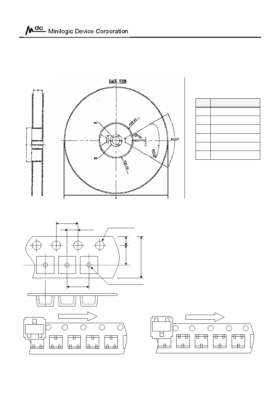
Packaging Information
Recommended Pattern Layout
0.4
-0.1
-0.05
(0.95)
1.9
± 0.2
2.9
± 0.2
1.6
-
0
.0
.1
+1
.2
2.
8
±
0.
2
1.1
± 0.1
mi
n.
0.
2
0 ~ 0.1
(0.8)
0.15
-0.1
-0.05
1.5
± 0.1
1.5
± 0.1
0.49
± 0.06
0.42
± 0.06
0.42
± 0.06
2.45
±
0.1
5
4.25
m
a
x
1.72
± 0.1
4.5
± 0.1
1.1 m
m
0.4
± 0.04
1.5
± 0.1
SOT-89 :
SOT-23 :
4.
2 m
a
x
1.27 1.27
5.2 max
5.
3 m
a
x
12
.7
m
i
n
TO-92 :
Units : mm
SOT-89
SOT-23 :
0.
9
1.
5
1.6
1.0
1. 0
3.
7
45∫
45∫
2.2
P10/14
0.
8
1.0
1.
9
2.4
ML61
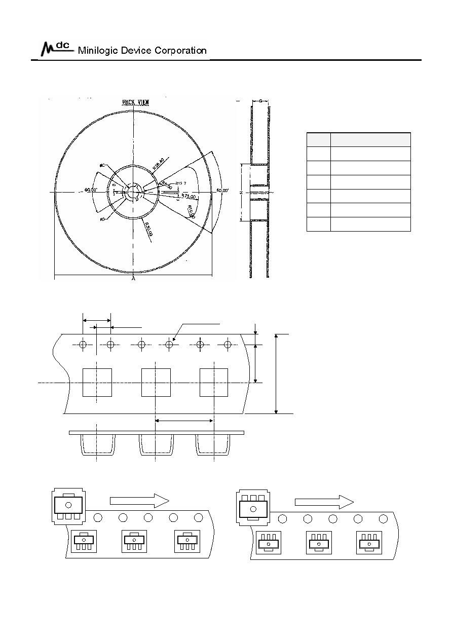
Tape and Reel Information
SOT-23 :
SIZE (mm)
A
178 ± 0.8
B
2
± 0.2
C
13 ± 0.2
D
21 ± 0.8
G
8
± 0.5
H
60
3,000 pcs / reel
SOT-23 Taping Specifications :
4
± 0.1
2
± 0.05
1.5
+ 0.1
- 0
1.1 ± 0.1
1.75
±
0.1
3.
5
±
0.
05
8
±
0.
2
4
± 0.1
Direction of feed
"R" type
[Orientation of Device: Right]
Standard Type
Direction of feed
"L" type
[Orientation of Device: Left]
Reverse Type
P11/14
ML61
SOT-89 :
SIZE (mm)
A
178 ± 0.8
B
2
± 0.2
C
13 ± 0.2
D
21 ± 0.8
G
12
± 0.5
H
60
1,000 pcs / reel
SOT-89 Taping Specifications :
4.0
± 0.1
1.
5
±
0.
1
5.
6
5
±
0
.
05
8.0
± 0.1
12
.
0
±
0.
2
2.0
± 0.05
1.5
+ 0.1
0
Direction of feed
"R" type
[Orientation of Device: Right]
Standard Type
"L" type
[Orientation of Device: Left]
Reverse Type
Direction of feed
P12/14

ML61
TO-92 Taping Specifications :
t
H1
P2
P
H
WO
W1
W
D
F
PO
W2
H0
L1
SIZE (mm)
P
12.7
± 1.0
PO
12.7
± 0.3
P2
6.35
± 0.4
F
2.5
W
18.0
± 1.0
WO
6.0
± 0.3
W1
9.0
± 0.5
W2 0.5
MAX
H
19.0
± 0.5
H0
16.0
± 0.5
H1 32.25
MAX
D
4.0 ± 0.2
t
0.6
± 0.2
L1 3.5
MIN
2,000 pcs / box
+ 0.45
- 0.15
P13/14

P14/14
ML61
History of Revision
REV DESCRIPTION DATE
First Official Specification
20/3/02
A
Modify Max. Output Current & Add Table of Electrical characteristics by
Detector Threshold.
3/4/02
B
Maximum Input Voltage increased to 12V, Hysteresis Range modified to 2% to
7% & Typical Performance Characteristics
31/10/02
C
Absolute Maximum Input Rating of Input Voltage reduced
from 12V to 10V.
3/9/04
The information presented in this document does not form part of any quotation or contract, is believed to be accurate and
reliable and may be changed without notice. No liability will be accepted by the publisher for any consequence of its use.