MIPS32TM 4KEcTM Processor Core Datasheet
November 8, 2002
MIPS32TM 4KEcTM Processor Core Datasheet, Revision 02.00
Document Number: MD00111
Copyright © 2001-2002 MIPS Technologies Inc. All rights reserved.
The MIPS32TM 4KEcTM core from MIPSÆ Technologies is a member of the MIPS32 4KETM processor core family. It is a
high-performance, low-power, 32-bit MIPS RISC core designed for custom system-on-silicon applications. The core is
designed for semiconductor manufacturing companies, ASIC developers, and system OEMs who want to rapidly integrate
their own custom logic and peripherals with a high-performance RISC processor. It is highly portable across processes, and
can be easily integrated into full system-on-silicon designs, allowing developers to focus their attention on end-user
products. The 4KEc core is ideally positioned to support new products for emerging segments of the digital consumer,
network, systems, and information management markets, enabling new tailored solutions for embedded applications.
The 4KEc core implements the MIPS32 Release 2 Architecture with the MIPS16eTM ASE, and the 32-bit privileged
resource architecture. The Memory Management Unit (MMU) contains 4-entry instruction and data Translation Lookaside
Buffers (ITLB/DTLB) and a 16 dual-entry joint TLB (JTLB) with variable page sizes.The synthesizable 4KEc core
includes a Multiply/Divide Unit (MDU) that implements single cycle MAC instructions, which enable DSP algorithms to
be performed efficiently. It allows 32-bit x 16-bit MAC instructions to be issued every cycle, while a 32-bit x 32-bit MAC
instruction can be issued every 2 cycles.
Instruction and data caches are fully configurable from 0 - 64 Kbytes in size. In addition, each cache can be organized as
direct-mapped or 2-way, 3-way, or 4-way set associative. Load and fetch cache misses only block until the critical word
becomes available. The pipeline resumes execution while the remaining words are being written to the cache. Both caches
are virtually indexed and physically tagged to allow them to be accessed in the same clock that the address is translated.
An optional Enhanced JTAG (EJTAG) block allows for single-stepping of the processor as well as instruction and data
virtual address/value breakpoints. Additionally, real-time tracing of instruction program counter, data address, and data
values can be supported.
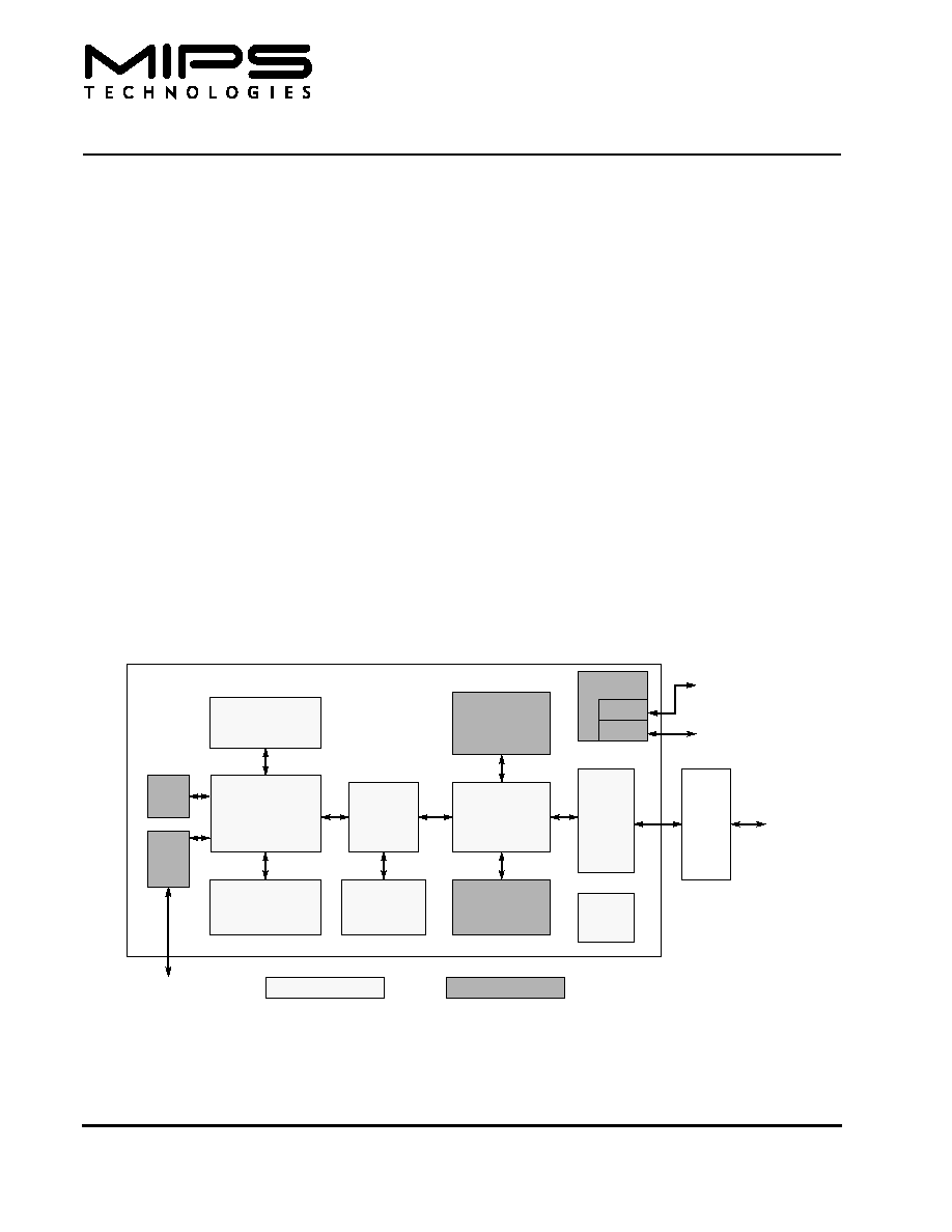
Figure 1
shows a block diagram of the 4KEc core. The core is divided into required and optional blocks as shown.
Figure 1 4KEc Core Block Diagram
System
Coprocessor
MDU
TLB
MMU
D-cache
BIU
TAP
EJTAG
Power
Mgmt
I-cache
Off-Chip
Debug I/F
Fixed/Required
Optional
Execution
Core
(RF/ALU/Shift)
Thin I/F
On-Chip Bus(es)
Trace
Off/On-Chip
Trace I/F
CP2
UDI
On-Chip
Coprocessor 2
Cache
Controller

2
MIPS32TM 4KEcTM Processor Core Datasheet, Revision 02.00
Copyright © 2001-2002 MIPS Technologies Inc. All rights reserved.
Features
∑ 5-stage pipeline
∑ 32-bit Address and Data Paths
∑ MIPS32-Compatible Instruction Set
≠
Multiply-Accumulate and Multiply-Subtract
Instructions (MADD, MADDU, MSUB, MSUBU)
≠
Targeted Multiply Instruction (MUL)
≠
Zero/One Detect Instructions (CLZ, CLO)
≠
Wait Instruction (WAIT)
≠
Conditional Move Instructions (MOVZ, MOVN)
≠
Prefetch Instruction (PREF)
∑ MIPS32 Enhanced Architecture (Release 2) Features
≠
Vectored interrupts and support for external interrupt
controller
≠
Programmable exception vector base
≠
Atomic interrupt enable/disable
≠
GPR shadow registers (optionally, one or three
additional shadows can be added to minimize latency
for interrupt handlers)
≠
Bit field manipulation instructions
≠
Improved virtual memory support (smaller page sizes
and hooks for more extensive page table manipulation)
∑ MIPS16eTM Code Compression
≠
16 bit encodings of 32 bit instructions to improve code
density
≠
Special PC-relative instructions for efficient loading of
addresses and constants
≠
SAVE & RESTORE macro instructions for setting up
and tearing down stack frames within subroutines
≠
Improved support for handling 8 and 16 bit datatypes
∑ Programmable Cache Sizes
≠
Individually configurable instruction and data caches
≠
Sizes from 0 - 64KB
≠
Direct Mapped, 2-, 3-, or 4-Way Set Associative
≠
Loads block only until critical word is available
≠
Write-back and write-through support
≠
16-byte cache line size
≠
Virtually indexed, physically tagged
≠
Cache line locking support
≠
Non-blocking prefetches
∑ Scratchpad RAM Support
≠
Can optionally replace 1 way of the I- and/or D-cache
with a fast scratchpad RAM
≠
Independent external pin interfaces for I- and D-
scratchpads
≠
20 index address bits allow access of arrays up to 1MB
≠
Interface allows back-stalling the core
∑ MIPS32 Privileged Resource Architecture
≠
Count/Compare registers for real-time timer interrupts
≠
I and D watch registers for SW breakpoints
∑ Programmable Memory Management Unit
≠
16 dual-entry JTLB with variable page size
≠
4-entry ITLB
≠
4-entry DTLB
∑ Simple Bus Interface Unit (BIU)
≠
All I/O's fully registered
≠
Separate unidirectional 32-bit address and data buses
≠
Two 16-byte collapsing write buffers
≠
Designed to allow easy conversion to other bus
protocols
∑ CorExtendTM User Defined Instruction Set Extensions
(available in 4KEc ProTM core)
≠
Allows user to define and add instructions to the core at
build time
≠
Maintains full MIPS32 compatibility
≠
Supported by industry standard development tools
≠
Single or multi-cycle instructions
≠
Separately licensed; a core with this feature is known as
the 4KEc ProTM core
∑ Multiply/Divide Unit
≠
Maximum issue rate of one 32x16 multiply per clock
≠
Maximum issue rate of one 32x32 multiply every other
clock
≠
Early-in iterative divide. Minimum 11 and maximum 34
clock latency (dividend (rs) sign extension-dependent)
∑ Coprocessor 2 interface
≠
32 bit interface to an external coprocessor
∑ Power Control
≠
Minimum frequency: 0 MHz
≠
Power-down mode (triggered by WAIT instruction)
≠
Support for software-controlled clock divider
≠
Support for extensive use of local gated clocks
∑ EJTAG Debug
≠
Support for single stepping
≠
Virtual instruction and data address/value breakpoints
≠
PC and data tracing
≠
TAP controller is chainable for multi-CPU debug
≠
Cross-CPU breakpoint support
∑ Testability
≠
Full scan design achieves test coverage in excess of
99% (dependent on library and configuration options)
≠
Optional memory BIST for internal SRAM arrays
Architecture Overview
The 4KEc core contains both required and optional blocks.
Required blocks are the lightly shaded areas of the block
diagram in
Figure 1
and must be implemented to remain
MIPS32TM 4KEcTM Processor Core Datasheet, Revision 02.00
3
Copyright © 2001-2002 MIPS Technologies Inc. All rights reserved.
MIPS-compliant. Optional blocks can be added to the
4KEc core based on the needs of the implementation.
The required blocks are as follows:
∑ Execution Unit
∑ Multiply/Divide Unit (MDU)
∑ System Control Coprocessor (CP0)
∑ Memory Management Unit (MMU)
∑ Transition Lookaside Buffer (TLB)
∑ Cache Controllers
∑ Bus Interface Unit (BIU)
∑ Power Management
Optional blocks include:
∑ Instruction Cache
∑ Data Cache
∑ Scratchpad RAM interface
∑ Coprocessor 2 interface
∑ CorExtendTM User Defined Instruction (UDI) support
∑ MIPS16e support
∑ Enhanced JTAG (EJTAG) Controller
The section entitled "4KEc Core Required Logic Blocks"
on page 4 discusses the required blocks. The section
entitled "4KEc Core Optional Logic Blocks" on page 15
discusses the optional blocks.
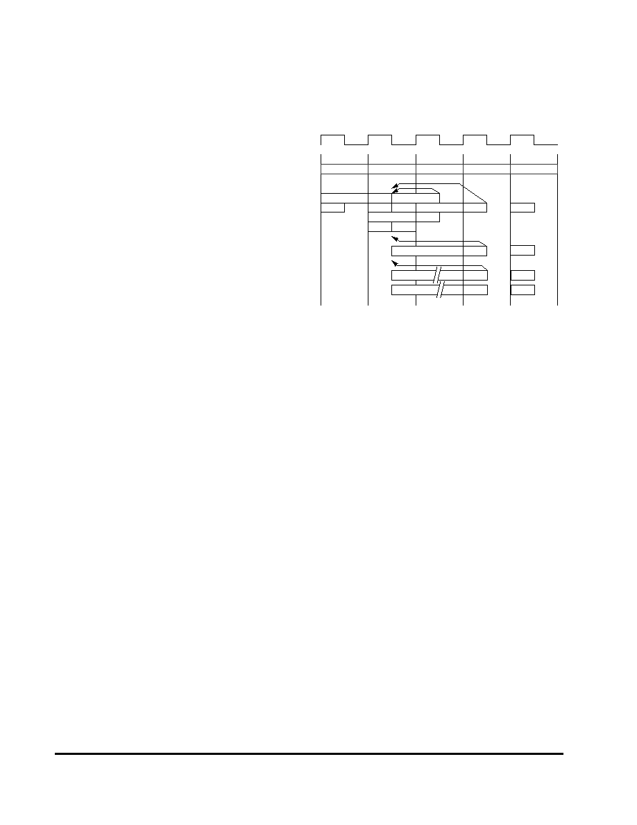
Pipeline Flow
The 4KEc core implements a 5-stage pipeline with
performance similar to the R3000
Æ
pipeline. The pipeline
allows the processor to achieve high frequency while
minimizing device complexity, reducing both cost and
power consumption.
The 4KEc core pipeline consists of five stages:
∑ Instruction (I Stage)
∑ Execution (E Stage)
∑ Memory (M Stage)
∑ Align (A Stage)
∑ Writeback (W stage)
The 4KEc core implements a bypass mechanism that
allows the result of an operation to be forwarded directly to
the instruction that needs it without having to write the
result to the register and then read it back.
Figure 2
shows a timing diagram of the 4KEc core pipeline.
Figure 2 4KEc Core Pipeline
I Stage: Instruction Fetch
During the Instruction fetch stage:
∑ An instruction is fetched from instruction cache.
∑ MIPS16e instructions are expanded into MIPS32-like
instructions
E Stage: Execution
During the Execution stage:
∑ Operands are fetched from register file.
∑ The arithmetic logic unit (ALU) begins the arithmetic
or logical operation for register-to-register instructions.
∑ The ALU calculates the data virtual address for load
and store instructions.
∑ The ALU determines whether the branch condition is
true and calculates the virtual branch target address for
branch instructions.
∑ Instruction logic selects an instruction address.
∑ All multiply and divide operations begin in this stage.
M Stage: Memory Fetch
During the Memory fetch stage:
∑ The arithmetic ALU operation completes.
∑ The data cache access and the data virtual-to-physical
address translation are performed for load and store
instructions.
I
E
M
A
W
I-TLB
I-A1
I-Cache
RegRd
I Dec
ALU Op
D-TLB
D-Cache
Align
RegW
D-AC
Bypass
Bypass
Mul-16x16, 32x16
RegW
Bypass
Acc
Mul-32x32
RegW
Acc
I-A2
Bypass
Div
RegW
Acc

4
MIPS32TM 4KEcTM Processor Core Datasheet, Revision 02.00
Copyright © 2001-2002 MIPS Technologies Inc. All rights reserved.
∑ Data cache look-up is performed and a hit/miss
determination is made.
∑ A 16x16 or 32x16 multiply calculation completes.
∑ A 32x32 multiply operation stalls the MDU pipeline
for one clock in the M stage.
∑ A divide operation stalls the MDU pipeline for a
maximum of 34 clocks in the M stage. Early-in sign
extension detection on the dividend will skip 7, 15, or
23 stall clocks.
A Stage: Align
During the Align stage:
∑ Load data is aligned to its word boundary.
∑ A 16x16 or 32x16 multiply operation performs the
carry-propagate-add. The actual register writeback is
performed in the W stage.
∑ A MUL operation makes the result available for
writeback. The actual register writeback is performed
in the W stage.
W Stage: Writeback
During the Writeback stage:
∑ For register-to-register or load instructions, the
instruction result is written back to the register file.
4KEc Core Required Logic Blocks
The 4KEc core consists of the following required logic
blocks, shown in
Figure 1
. These logic blocks are defined
in the following subsections:
∑ Execution Unit
∑ Multiply/Divide Unit (MDU)
∑ System Control Coprocessor (CP0)
∑ Memory Management Unit (MMU)
∑ Transition Lookaside Buffer (TLB)
∑ Cache Controller
∑ Bus Interface Unit (BIU)
∑ Power Management
Execution Unit
The 4KEc core execution unit implements a load/store
architecture with single-cycle ALU operations (logical,
shift, add, subtract) and an autonomous multiply/divide
unit. The 4KEc core contains thirty-two 32-bit general-
purpose registers used for integer operations and address
calculation. Optionally, one or three additional register file
shadow sets (each containing thirty-two registers) can be
added to minimize context switching overhead during
interrupt/exception processing. The register file consists of
two read ports and one write port and is fully bypassed to
minimize operation latency in the pipeline.
The execution unit includes:
∑ 32-bit adder used for calculating the data address
∑ Address unit for calculating the next instruction
address
∑ Logic for branch determination and branch target
address calculation
∑ Load aligner
∑ Bypass multiplexers used to avoid stalls when
executing instructions streams where data producing
instructions are followed closely by consumers of their
results
∑ Leading Zero/One detect unit for implementing the
CLZ and CLO instructions
∑ Arithmetic Logic Unit (ALU) for performing bitwise
logical operations
∑ Shifter & Store Aligner
Multiply/Divide Unit (MDU)
The 4KEc core includes a multiply/divide unit (MDU) that
contains a separate pipeline for multiply and divide
operations. This pipeline operates in parallel with the
integer unit (IU) pipeline and does not stall when the IU
pipeline stalls. This setup allows long-running MDU
operations, such as a divide, to be partially masked by
system stalls and/or other integer unit instructions.
The MDU consists of a 32x16 booth recoded multiplier,
result/accumulation registers (HI and LO), a divide state
machine, and the necessary multiplexers and control logic.
The first number shown (`32' of 32x16) represents the rs
operand. The second number (`16' of 32x16) represents the
rt operand. The 4KEc core only checks the value of the
latter (rt) operand to determine how many times the
operation must pass through the multiplier. The 16x16 and
32x16 operations pass through the multiplier once. A
32x32 operation passes through the multiplier twice.
The MDU supports execution of one 16x16 or 32x16
multiply operation every clock cycle; 32x32 multiply
MIPS32TM 4KEcTM Processor Core Datasheet, Revision 02.00
5
Copyright © 2001-2002 MIPS Technologies Inc. All rights reserved.
operations can be issued every other clock cycle.
Appropriate interlocks are implemented to stall the
issuance of back-to-back 32x32 multiply operations. The
multiply operand size is automatically determined by logic
built into the MDU.
Divide operations are implemented with a simple 1 bit per
clock iterative algorithm. An early-in detection checks the
sign extension of the dividend (rs) operand. If rs is 8 bits
wide, 23 iterations are skipped. For a 16-bit-wide rs, 15
iterations are skipped, and for a 24-bit-wide rs, 7 iterations
are skipped. Any attempt to issue a subsequent MDU
instruction while a divide is still active causes an IU
pipeline stall until the divide operation is completed.
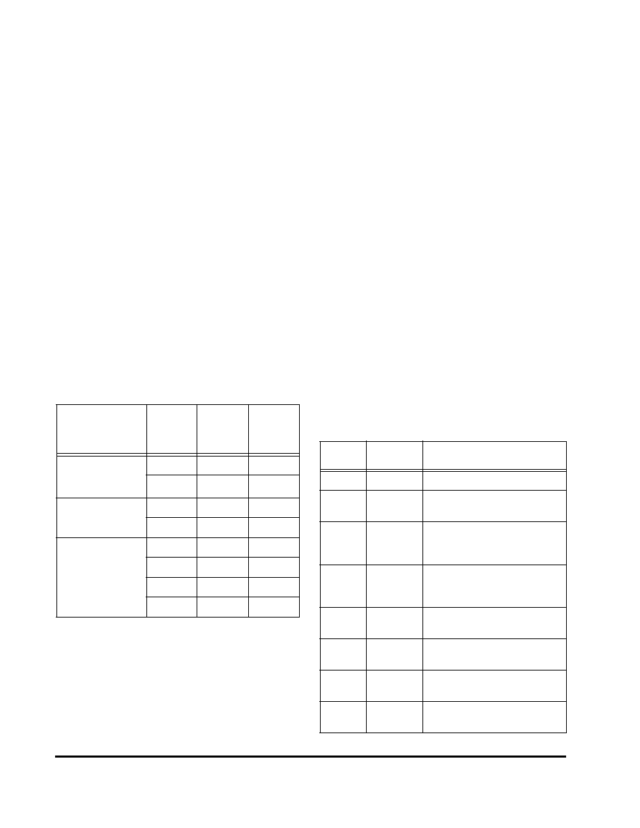
Table 1 lists the repeat rate (peak issue rate of cycles until
the operation can be reissued) and latency (number of
cycles until a result is available) for the 4KEc core multiply
and divide instructions. The approximate latency and
repeat rates are listed in terms of pipeline clocks. For a
more detailed discussion of latencies and repeat rates, refer
to Chapter 2 of the MIPS32 4KETM Processor Core Family
Software User's Manual.
The MIPS architecture defines that the result of a multiply
or divide operation be placed in the HI and LO registers.
Using the Move-From-HI (MFHI) and Move-From-LO
(MFLO) instructions, these values can be transferred to the
general-purpose register file.
In addition to the HI/LO targeted operations, the MIPS32
architecture also defines a multiply instruction, MUL,
which places the least significant results in the primary
register file instead of the HI/LO register pair. By avoiding
the explicit MFLO instruction, required when using the LO
register, and by supporting multiple destination registers,
the throughput of multiply-intensive operations is
increased.
Two other instructions, multiply-add (MADD) and
multiply-subtract (MSUB), are used to perform the
multiply-accumulate and multiply-subtract operations. The
MADD instruction multiplies two numbers and then adds
the product to the current contents of the HI and LO
registers. Similarly, the MSUB instruction multiplies two
operands and then subtracts the product from the HI and
LO registers. The MADD and MSUB operations are
commonly used in DSP algorithms.
System Control Coprocessor (CP0)
In the MIPS architecture, CP0 is responsible for the virtual-
to-physical address translation and cache protocols, the
exception control system, the processor's diagnostics
capability, the operating modes (kernel, user, and debug),
and whether interrupts are enabled or disabled.
Configuration information, such as cache size and set
associativity, is also available by accessing the CP0
registers, listed in Table 2.
Table 1
4KEc Core High-Performance Integer Multiply/
Divide Unit Latencies and Repeat Rates
Opcode
Operand
Size
(mul
rt)
(div
rs)
Latency
Repeat
Rate
MULT/MULTU,
MADD/MADDU,
MSUB/MSUBU
16 bits
1
1
32 bits
2
2
MUL
16 bits
2
1
32 bits
3
2
DIV/DIVU
8 bits
12
11
16 bits
19
18
24 bits
26
25
32 bits
33
32
Table 2 Coprocessor 0 Registers in Numerical Order
Register
Number
Register
Name
Function
0
Index
3
Index into the TLB array.
1
Random
3
Randomly generated index into the
TLB array.
2
EntryLo0
3
Low-order portion of the TLB
entry for odd-numbered virtual
pages.
3
EntryLo1
3
Low-order portion of the TLB
entry for odd-numbered virtual
pages.
4
Context
1
Pointer to page table entry in
memory.
4
Context-
Config
1
Controls the layout of the Context
register.
5
PageMask
3
Control for variable page sizes in
TLB entries.
5
PageGrain
3
Controls the layout of the EntryLo,
PageMask and EntryHi registers.