1
Features
∑
FAX and Modem interface (V.34/V.34+)
∑
Designed to work at data rates up to 56kbits
∑
External programmable line and network
balance impedances
∑
Programmable DC termination characteristics
∑
IEC950 recognised component
∑
Transformerless 2-4 Wire conversion
∑
Integral Loop Switch
∑
Dial Pulse and DTMF operation
∑
Accommodates parallel phone detection
∑
Line state detection outputs:
-loop current/ringing voltage/line voltage
∑
+5V operation, low on-hook power (25mW)
∑
Full duplex voice and data transmission
∑
On-Hook reception from the line
∑
Meets French current limit requirements
∑
Conforms to German dial pulse standards
∑
Approvable to UL 1950
∑
Industrial Temperature Range Available
Applications
Interface to Central Office or PABX line for:
∑
FAX/Modem
∑
Electronic Point of Sale
∑
Security System
∑
Telemetry
∑
Set Top Boxes
Description
The Mitel MH88437 Data Access Arrangement
(D.A.A.) provides a complete interface between
audio or data transmission equipment and a
telephone line. All functions are integrated into a
single thick film hybrid module which provides high
voltage isolation, very high reliability and optimum
circuit design, needing a minimum of external
components.
The impedance and network balance are externally
programmable, as are the DC termination
characteristics, making the device suitable for most
countries worldwide.
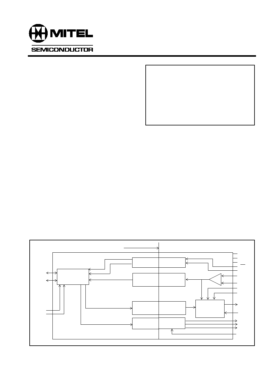
Figure 1 - Functional Block Diagram
Opto-
Isolation
Logic Input
Buffer
Isolation
Isolation
Isolation
Analog
Buffer
Analog
Buffer
Buffer
THL cancellation
impedance
matching circuit
Isolation Barrier
VCC
AGND
LC
VR+
VX
RV
TIP
RING
User Connections
Network Connections
Input Buffer
&
VLOOP1
Ring & Loop
Line Termination
VLOOP2
VR-
NB1
NB2
LOOP
LCD
ZA
RS
VBIAS
and line
CL
DS5060
ISSUE 4
October 1998
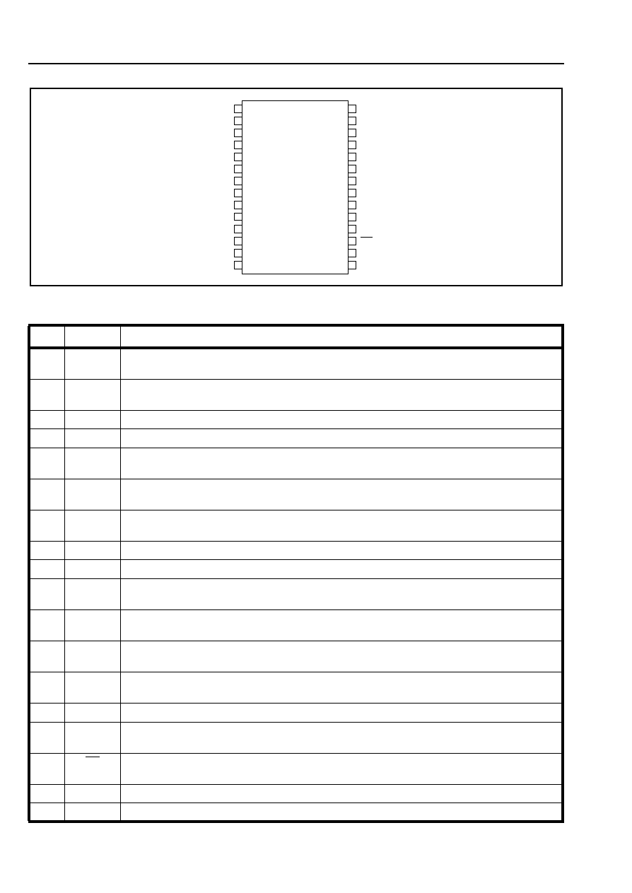
Package Information
MH88437AD-P 28 Pin DIL Package
MH88437AS-P 28 Pin SM Package
0∞C to 70∞C
MH88437AD-PI Ind. Temp. DIL Variant
-40∞C to +80∞C
MH88437AS-PI Ind. Temp. SM Variant
-40∞C to + 80∞C
MH88437-P
Data Access Arrangement
Advance Information
MH88437-P
Advance Information
2
Figure 2 - Pin Connections
Pin Description
Pin #
Name
Description
1
NB1
Network Balance 1. External passive components must be connected between this pin and
NB2.
2
NB2
Network Balance 2. External passive components must be connected between this pin and
NB1.
3
VR+
Differential Receive (Input). Analog input from modem/fax chip set.
4
VR-
Differential Receive (Input). Analog input from modem/fax chip set.
5
VX
Transmit (Output). Ground referenced (AGND) output to modem/fax chip set, biased at
+2.0V.
6
LC
Loop Control (Input). A logic 1 applied to this pin activates internal circuitry which provides
a DC termination across Tip and Ring. This pin is also used for dial pulse application.
7
ZA
Line Impedance. Connect impedance matching components from this pin to Ground
(AGND).
8
AGND
Analog Ground. 4-Wire 0V reference connect to mains earth (ground).
9
V
CC
Positive Supply Voltage. +5V.
10
VBIAS
Internal Reference Voltage. +2.0V reference voltage. This pin should be decoupled
externally to AGND, typically with a 10
µ
F
6.3V capacitor
.
11
LOOP
Loop (Output). The output voltage on this pin is proportional to the line voltage across Tip -
Ring, scaled down by a factor of 50.
12,
14
IC
Internal Connection. No connection should be made to this pin externally.
13
RS
Ringing Sensitivity. Connecting a link or resistor between this pin and LOOP (pin 11) will
vary the ringing detection sensitivity of the module.
15
LCD
Loop Condition Detect (Output). Indicates the status of loop current.
16
RV
Ringing Voltage Detect (Output). The RV output indicates the presence of a ringing voltage
applied across the Tip and Ring leads.
17
CL
Current Limit. A logic 0 applied to this pin activates internal circuitry which limits the loop
current.
18
NP
No Pin. Isolation Barrier, fitted, no pin fitted in this position.
19
NP
No Pin. Isolation barrier, no pin fitted in this position
CL
IC
LC
IC
TIP
AGND
RING
RV
ZA
VX
VR-
VCC
1
2
3
4
5
6
7
8
9
10
11
12
13
14
28
27
26
25
24
23
22
21
20
19
18
17
16
15
VR+
NB1
NB2
VBIAS
LOOP
IC
RS
IC
VLOOP1
VLOOP2
IC
SC
SC
NP
NP
LCD

Advance Information
MH88437-P
3
20,23
26
IC
Internal Connection. No connection should be made to this pin externally.
21,22
SC
Short Circuit. These two pins should be connected to each other via a 0
link.
24
VLOOP2
Loop Voltage Control Node 2. Used to set DC termination characteristics.
25
VLOOP1
Loop Voltage Control Node 1. Used to set DC termination characteristics.
27
RING
Ring Lead. Connects to the "Ring" lead of the telephone line.
28
TIP
Tip Lead. Connects to the "Tip" lead of the telephone line.
Pin Description (continued)
Pin #
Name
Description
Functional Description
The device is a Data Access Arrangement (D.A.A.). It
is used to correctly terminate a 2-Wire telephone
line. It provides a signalling link and a 2-4 Wire line
interface between an analog loop and subscriber
data transmission equipment, such as Modems,
Facsimiles (Fax's), Remote Meters, Electronic Point
of Sale equipment and Set Top Boxes.
Isolation Barrier
The device provides an isolation barrier capable of
meeting the supplementary barrier requirements of
the international standard IEC 950 and the national
variants of this scheme such as EN 60950 for
European applications and UL 1950 for North
American applications.
External Protection Circuit
An External Protection Circuit assists in preventing
damage to the device and the subscriber equipment,
due to over-voltage conditions. See Application Note
MSAN-154 for recommendations.
Suitable Markets
The MH88437 has features such as programmable
line and network balance impedance, programmable
DC termination and a supplementary isolation
barrier. For countries that do not need to meet the
French and German requirements there is a pin for
pin compatible device the MH88435.
There are, however, a small number of countries with
a 100M
leakage requirement that this device does
not meet. These are Belgium, Greece, Italy,
Luxembourg, Spain and Poland. Although
Luxembourg will now accept TBR21 and there are
exceptions to the Italian specification, in most
applications the MH88437 will comply with
Luxembourg and Italian specifications. For approval
in Denmark and Sweden the TRB21 route is
recommended.
Approval specifications are regularly changing and
the relevant specification should always be consulted
before commencing design.
Line Termination
When Loop Control (LC) is at a logic 1, a line
termination is applied across Tip and Ring. The
device can be considered off-hook and DC loop
current will flow. The line termination consists of both
a DC line termination and an AC input impedance. It
is used to terminate an incoming call, seize the line
for an outgoing call, or if it is applied and
disconnected at the required rate, can be used to
generate dial pulses.
The DC termination resembles approximately 300
resistance, which is loop current dependent.
Furthermore, it can be programmed to meet different
national requirements. For normal operation
VLOOP3 should be open circuit and a resistor (R2)
should be fitted between VLOOP1 and VLOOP2, as
shown in Figure 4.
The approval specification will give a DC mask
characteristic that the equipment will need to comply
to. The DC mask specifies the amount of current the
DAA can sink for a given voltage across tip and ring.
Graph 1 shows how the voltage across tip and ring
varies with different resistors (R2) for a given loop
current.
Network Balance
The network balance impedance of the device can
be programmed by adding external components By

MH88437-P
Advance Information
4
applying a logic 0 to Pin 17, CL, the loop current will
be limited to below 60mA as required in France and
the European TBR21 specification. For all other
countries where current limiting is not required, CL
should be set to 1.
The AC input impedance should be set by the user to
match the line impedance.
Input Impedance
The MH88437 has a programmable input impedance
set by fitting external components between the ZA
pin and AGND.
For complex impedances the configuration shown in
Figure 4 (below) is most commonly found.
Figure 4 - Complex Impedances
To find the external programming components for
configuration 4, the following formula should be
used:
Zext = [(10 x R1)-1k3]+[(10 x R2)//(C1/10)]
e.g. If the required input impedance = 220
+ (820
/
/115nF), the external network to be connected to ZA
will be:
ZA = 900
+
(8k2
//12nF)
Where the input impedance (Z) = 600R the equation
can be simplified to:
ZA = (10 x Z) - 1k3
ZA = 4k7
Note: A table of commonly used impedances can be
found in the DAA Application's document MSAN-154.
Where Zext = external network connected between
ZA and AGND and Zint = 1.3k
(internal resistance)
between NB1 and NB2. For countries where the
balance impedance matches the line impedance, a
16k
resistor should be added between NB1 and
NB2.
R1
R2
C1
Figure 3 - DC Programming Capability
Iloop=15mA
Iloop=20mA
Iloop=26mA
35
30
10
5
0
25
20
15
40
50
150 250 350 450 550 650 750 850 950
R2(kOhms)
V(t-r)

Advance Information
MH88437-P
5
Ringing Voltage Detection
The sensitivity of the ringing voltage detection
circuitry can be adjusted by applying an external
resistor (R7, Figure 5) between the RS and LOOP
pins. With a short circuit, the threshold sensitivity is
~10Vrms, therefore R7 = 30k
x (Desired threshold
voltage - 10Vrms).
Example: 300k
gives ~20Vrms and 600k
gives
~30Vrms.
An AC ringing voltage across Tip and Ring will cause
RV to output TTL pulses at the ringing frequency,
with an envelope determined by the ringing cadence.
Parallel Phone and Dummy Ringer
An external parallel phone or dummy ringer circuit
can be connected across Tip and Ring as shown in
Figure 5. A Dummy Ringer is an AC load which
represents a telephone's mechanical ringer.
In normal circumstances when a telephone is On-
Hook and connected to the PSTN, its AC (Ringer)
load is permanently presented to the network. This
condition is used by many PTT's to test line
continuity, by placing a small AC current onto the line
and measuring the voltage across tip (A) and ring
(B).
Today's telecom equipment may not have an AC load
present across tip and ring (e.g. modems), therefore
any testing carried out by the PTT will see an open
circuit across tip and ring. In this instance the PTT
assumes that the line continuity has been damaged.
To overcome this problem many PTT's specify that a
"Dummy Ringer" is presented to the network at all
times. Ideally its impedance should be low in the
audio band and high at the ringing frequencies (e.g.
25Hz). Note that the requirement for the "Dummy
Ringer" is country specific.
Parallel phone detection is used mostly in set-top
box applications. This is when a modem call will
need to be disconnected from the central office by
the equipment when the parallel phone is in the off-
hook state. This is to allow the subscriber to make
emergency calls.
To detect this state, additional circuitry will be
required. Refer to Application Note MSAN-154.
2-4 Wire Conversion
The device converts the balanced 2-Wire input,
presented by the line at Tip and Ring, to a ground
referenced signal at VX, biased at 2.0V. This
simplifies the interface to a modem chip set.
Conversely, the device converts the differential signal
input at VR+ and VR- to a balanced 2-Wire signal at
Tip and Ring. The device can also be used in a
single ended mode at the receive input, by leaving
VR+ open circuit and connecting the input signal to
VR- only. Both inputs are biased at 2.0V.
During full duplex transmission, the signal at Tip and
Ring consists of both the signal from the device to
the line and the signal from the line to the device.
The signal input at VR+ and VR- being sent to the
line, must not appear at the output VX. In order to
prevent this, the device has an internal cancellation
circuit, the measure of this attenuation is Transhybrid
Loss (THL).
The MH88437 has the ability to transmit analog
signals from Tip and Ring through to VX when on-
hook. This can be used when receiving caller line
identification information.
Transmit Gain
The Transmit Gain of the MH88437 is the gain from
the differential signal across Tip and Ring to the
ground referenced signal at VX. The internal
Transmit Gain of the device is fixed as shown in the
AC Electrical Characteristics table. For the correct
gain, the Input Impedance of the MH88437, must
match the specified line impedance.
By adding an external potential divider to VX, it is
possible to reduce the overall gain in the application.
The output impedance of VX is approximately 10
and the minimum resistance from VX to ground
should be 2k
.
Example: If R3 = R4 = 2k
,
in Figure 5, the overall
gain would reduce by 6.0dB.
Receive Gain
The Receive Gain of the MH88437 is the gain from
the differential signal at VR+ and VR- to the
differential signal across Tip and Ring. The internal
Receive Gain of the device is fixed as shown in the
AC Electrical Characteristics table. For the correct