
2-269
Æ
Features
∑
Input impedance variants:
- 600
- 200
+ 680
// 0.1
µ
F
- 200
+ 560
// 0.1
µ
F
∑
Operates with a wide range of battery voltages
∑
Constant current battery feed with constant
voltage fallback for long loop drive capabilities
∑
Overvoltage and short circuit protection
∑
Off-hook detection and LED indicator drive
∑
Dial pulse detection
∑
Ring trip filter with auto ring trip
∑
Ring relay driver plus three more uncommitted
relay drivers
∑
Transformerless 2W to 4W conversion
∑
A/D and D/A conversion
∑
Conforms to A-Law PCM
∑
Analog and digital loopback
∑
Conforms to CCITT k.20 overvoltage surge
requirements with external primary protection
circuitry
Applications
∑
Off premise digital PBX line cards
∑
DID (Direct Inward Dial) line cards
∑
PABX, Key Systems, Central Office Equipment
Description
The Mitel MH89625C SLIC (Subscriber Line
Interface Circuit) provides a complete interface
between an off-premise telephone line and a digital
switching system. All BORSCHT functions of Battery
Feed, Overvoltage Protection, Ringing Feed, Line
Supervision, Codec, 2-4 Wire Hybrid and Test are
provided requiring only a few external components.
The input impedance conforms with Chinese
standard requirements. The device is fabricated
using thick film hybrid technology which incorporates
various technologies for high voltage capability,
optimum circuit design and very high reliability.
Figure 1 - Functional Block Diagram
TIP
RING
RF2
RF1
VBat
LGND
LCA
GS
VREF
CA
DSTo
DSTi
CSTi
F1i
C2i
RD4
RD3
RD2
RD1
SHK
LED
Gain
Adjust
2w/4w
hybrid
Impedance
Matching
Relay
Driver 1
Relay
Driver 2
Relay
Driver 3
Relay
Driver 4
Line
Supervision
Ring
Trip
Filter
Tip
Drive
Current
& Voltage
Sensing
Ring
Drive
Constant
Current &
Voltage
Control
VREF
CA
DSTo
DSTi
CSTi
F1i
CS
SD3
SD2
SD1
SD0
CODEC
VX
VR
ISSUE 4
May 1995
Ordering Information
MH89625C
600
MH89625C- 5
200
+ 680
// 0.1
µ
F
MH89625C- 6
200
+ 560
// 0.1
µ
F
40 Pin DIL Package
MH89625C
OPS/DID PCM SLIC
Preliminary Information
2-270
MH89625C
Preliminary Information
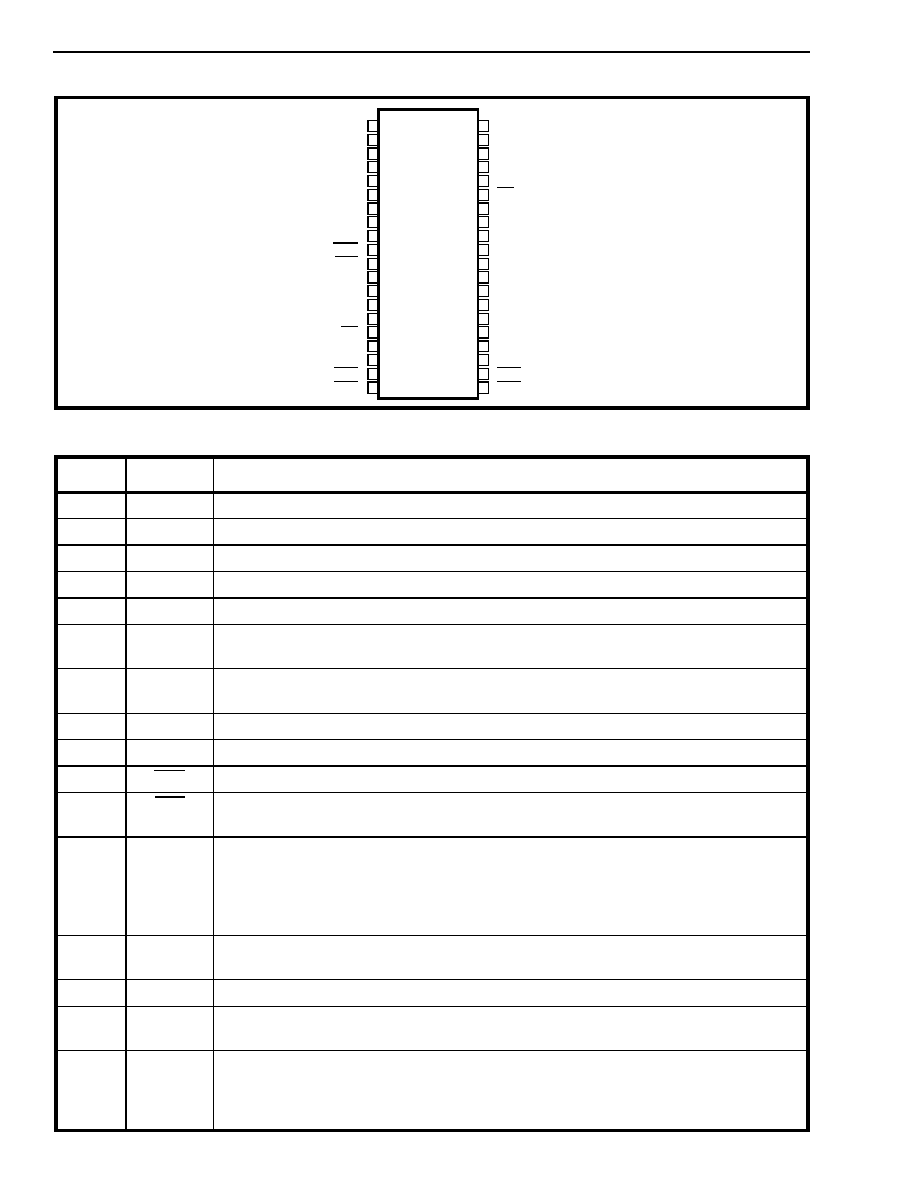
Figure 2 - Pin Connections
Pin Description
Pin #
Name
Description
1
TIP
Tip Lead. Connects to the "Tip" lead of the telephone line.
2
RING
Ring Lead. Connects to the "Ring" lead of the telephone line.
3
IC
Internal Connection: This pin is internally connected.
4
IC
Internal Connection: This pin is internally connected.
5
IC
Internal Connection: This pin is internally connected.
6
RF1
Ring Feed 1: For OPS operation, connects to the external battery backed ringing
generator, see Figure 2.
7
RF2
Ring Feed 2: For OPS operation, connects to RING through a normally closed relay
contact (K1), see Figure 2.
8
IC
Internal Connection. This pin is internally connected.
9
V
EE
Negative Supply Voltage: (-5V)
10
SHK
Switch Hook Detect (Output): A logic low indicates an off-hook condition.
11
LED
LED Drive (Output): Drives an LED directly through an internal 2.2k
resistor. A logic
low indicates an off-hook condition.
12
CSTi
Control ST-BUS in (Input): A TTL compatible digital input used to control the function
of the filter/codec. Three modes of operation may be affected by applying to this input
logic high, logic low or an 8-bit serial word, depending on the logic states of CA and F1i.
Functions controlled are: power down, filter gain adjust, loopback, chip testing, and the
SD outputs which control the relay drivers, ring trip circuitry and impedance selection.
13
DSTi
Data ST-BUS in (Input): A TTL compatible digital input which accepts the 8-bit PCM
word from the incoming PCM bus.
14
C2i
Clock Input (Input): A TTL compatible digital input which accepts the 2048 kHz clock.
15
DSTo
Data ST-BUS Out (Output). A three stage TTL compatible digital output which drives
the 8-bit PCM word to the outgoing PCM bus.
16
F1i
Synchronization Input (Input): A TTL compatible active low digital input enabling (in
conjunction with CA) the PCM input, PCM output and digital control input. It is internally
sampled on every positive edge of the clock, C2i, and provides frame and channel
synchronization.
IC
IC
VBAT
LGND
GS
VAC
IC
LCA
VDD
AGND
IC
IC
IC
IC
IC
VREF
VRLY
RD4
RD3
IC
RING
IC
IC
IC
RF1
RF2
IC
VEE
SHK
LED
CSTi
DSTi
C2i
DSTo
F1i
CA
RGND
RD2
RD1
TIP
2
3
4
5
6
7
8
9
10
11
12
13
14
15
16
17
18
19
20
40
39
38
37
36
35
34
33
32
31
30
29
28
27
26
25
24
23
22
21
1

2-271
Preliminary Information
MH89625C
17
CA
Control Address (Input): A three-level digital input which enables PCM input and
output, and determines into which control register (A or B) the serial data, presented to
CSTi, is stored.
18
RGND
Relay Ground: Return path for relay supply voltage.
19
RD2
Relay Driver 2: Connects to a user provided external relay coil. A logic high at the SD1
output of the internal MT8967 codec activates this driver. An internal clamp diode from
VRLY to RD2 is provided. This relay is typically used for DID reversals.
20
RD1
Relay Driver 1. Connects to a user provided external relay coil. A logic high at the SD0
output of the internal MT8967 codec activates this driver. An internal clamp diode from
VRLY to RD1 is provided. This relay is typically used for ringing.
21
RD3
Relay Driver 3. Connects to a user provided external relay coil. A logic high at the SD2
output of the internal MT8967 codec activates this driver. An internal clamp diode from
VRLY to RD3 is provided. This relay is typically used for in-test.
22
RD4
Relay Driver 4: Connects to a user provided external relay coil. A logic high at the SD3
output of the internal MT8967 codec activates this driver. An internal clamp diode from
VRLY to RD4 is provided. This relay is typically used for out-test.
23
V
RLY
Relay Positive Supply Voltage: Normally +5V. Connects to the relay coil and the relay
supply voltage.
24
V
Ref
Voltage Reference (Input): +2.50V for the internal codec.
25
IC
Internal Connection: This pin is internally connected.
26
IC
Internal Connection: This pin is internally connected
27
IC
Internal Connection: This pin is internally connected
28
IC
Internal Connection: This pin is internally connected
29
IC
Internal Connection: This pin is internally connected
30
AGND
Analog Ground. Analog and Digital Ground. Connects to System Ground.
31
V
DD
Positive Supply Voltage (+5V)
32
LCA
Loop Current Adjust (Input). The maximum constant loop current is a function of the
resistance connected from this pin to V
EE
. Normally left open
33
IC
Internal Connection. This pin is internally connected.
34
VAC
Battery AC Component (Input). AC noise present in the V
BAT
supply, isolated from the
DC component, can be applied to this pin to reduce longitudinal noise on TIP and RING.
To implement this feature, connect a 0.1
µ
F 100V capacitor from V
BAT
to VAC, and a 1k
resistor from VAC to AGND. This pin must be tied to AGND when not used.
35
GS
Gain Setting (Input). A logic low at this input adds an additional -0.5dB gain in the
receive direction (DSTi to Tip-Ring). This gain is in addition to the gain set by the Codec.
A logic high adds 0dB gain.
36
LGND
Loop Ground. Return path for the battery (V
BAT
) supply voltage. Connects to System
Ground.
37
V
Bat
Battery Supply Voltage. Normally -48V.
38
IC
Internal Connection: This pin is internally connected
39
IC
Internal Connection: This pin is internally connected
40
IC
Internal Connection: This pin is internally connected
Pin Description (Continued)
Pin #
Name
Description

2-272
MH89625C
Preliminary Information
Functional Description
The Mitel MH89625C OPS SLIC (Off-Premise
Subscriber Line Interface Circuit) provides a
complete interface between an off-premise
telephone line and an digital switching system. All
BORSCHT functions are provided requiring only a
few external components. The input impedance
conforms with Chinese standard requirements.
All functions of the SLIC are controlled by the system
Drive (SD) outputs of the internal Mitel A-Law Codec
MT8967. The SD outputs are controlled by the serial
data input stream at CSTi.
The BORSCHT Functions
The MH89625C performs all of the BORSCHT
functions of Battery Feed, Overvoltage Protection,
Ringing, Supervision, Codec, Hybrid and Test.
Battery Feed
The MH89625C powers the telephone set with
constant DC loop current for short lines and
automatically reverts to constant voltage for long
lines. The constant loop current is a function of the
resistance connected from the LCA pin to V
EE.
Where I
Loop
is the desired constant loop current in mA,
and R is the resistance from pin LCA to pin V
EE
in
ohms.
Overvoltage Protection
The MH89625C is protected from short term (20ms)
transients (+250V) between TIP and RING, TIP and
ground, and RING and ground. However, additional
protection circuitry may be needed depending on the
requirements which must be met. Normally simple
external shunt protection as shown in Figure 4 is all
that is required.
R (k
)
open
348k
200k
80k
50k
30k
I
Loop
(mA)
22.0
25.0
27.1
34.0
40.2
49.7
147.2 -I
Loop
(0.0001176 X I
Loop
) -0.002586
R =
Ringing
The ringing insertion circuit has the capability to
provide ringing voltage to a telephone set by simply
adding an external relay, ring generator and a
transient protector. The internal relay driver switches
ringing voltage onto the line via the external ring
relay. A clamp diode is included which suppresses
voltage transients during relay switching caused by
the relay coil. The serial data input at CSTi controls
the internal Codec's SDo output which activates the
ring driver. Refer to Table 1 for control of SLIC
functions.
Supervision
The loop detection circuit determines whether a low
enough resistance is across Tip and Ring to be
recognized as an off-hook condition. When an
off-hook condition occurs, the SHK and LED (the
LED output can drive an LED directly) outputs toggle
to a low level. These outputs also toggle with
incoming dial pulses.
During applied ringing (ring relay driver activated),
the loop detection circuit engages a ringing filter.
This filter prevents false off-hook detection due to
the current associated with the AC ringing voltage as
well as current transients that occur when the ringing
voltage is switched in and out. The ring trip detection
circuitry deactivates the ring relay driver after an
off-hook condition is detected.
Codec
The Codec function of the SLIC is implemented
using the Mitel MT8967 A-Law Codec. This device
provides the conversion interface between the
voiceband analog signals of a telephone subscriber
loop and the digital signals required in a digital PCM
(pulse code modulation) system. Eight-bit PCM
encoded digital data enters and leaves the chip
serially on DSTi and DSTo pins, respectively.
For detailed information on the CODEC portion of
the MH89625C, refer to the MT8967 integrated PCM
Filer/Codec data sheet (Microelectronics Digital
Communications Handbook, Mitel Semiconductor
Issue 9).

2-273
Preliminary Information
MH89625C
.
* Exceeding these values may cause permanent damage. Functional operation under these conditions is not implied.
x
LGND is connected to AGND
x
LGND is connected to AGND.
y
Temperature coefficient of V
REF
should be better than 100ppm/C.
Typical figures are at 25∞C and are for design aid only: not guaranteed and not subject to production testing.
Absolute Maximum Ratings* -
All voltages are with respect to AGND unless otherwise specified.
Parameter
Symbol
Min
Max
Units
1
DC Supply Voltage
V
DD
V
EE
-0.3
0.3
7
-7
V
2
DC Battery Voltage
x
V
BAT
0.3
-65
V
3
DC Ring Relay Voltage
V
RLY
-0.3
7
V
4
DC Reference Voltage
V
REF
-0.3
V
DD
V
5
AC Ring Generator Voltage
150
V
RMS
6
DC Digital Input Voltage
GS, CSTi
DSTi, C2i
F1i
-0.3
V
DD
V
7
DC Digital (3-level) Input voltage
CA
V
EE
V
DD
V
8
Storage Temperature
TS
-40
+125
∞C
Recommended Operating Conditions
Parameters
Sym
Min
Typ
Max
Units
Test Conditions
1
DC Supply Voltages
V
DD
V
EE
4.75
-4.75
5.0
-5.0
5.25
-5.25
V
V
2
DC Battery Voltage
x
V
BAT
-39.8
-48
-60
V
3
DC Ring Relay Voltage
V
RLY
5.0
7
V
4
DC Reference Voltage
y
V
REF
2.488
2.500
2.512
V
5
AC Ringing Generator
Voltage
Ringing Generator
Frequency
22
90
25
130
28
V
RMS
Hz
6
Operating Temperature
T
OP
0
25
70
∞C

2-274
MH89625C
Preliminary Information
DC Electrical Characteristics are over Recommended Operating Conditions with V
DD
at +5.0V ± 5% and V
EE
at -5.0V ±5% unless otherwise
stated.
Typical figures are at 25
∞
C with nominal ± 5V supplies and are for design aid only.
x
Supply current and power consumption characteristics are over Recommended Operating Conditions with V
DD
at 5.0V, V
EE
at -5.0V
and V
BAT
at -48.0V
y
The LED output consists of a 2.2k
resistor in series with the SHK HCT output.
NOTE 1: Powerdown mode is activated through the CSTi input data stream. Refer to Table 2.
DC Electrical Characteristics
Characteristics
Sym
Min
Typ
Max
Units
Test Conditions
1
Supply and Battery Current
x
Short Loop
Open Loop
I
DD
I
EE
I
BAT
I
BAT
8.7
8.4
23.5
1.5
15
15
28
2
mA
mA
mA
mA
LCA = Open
R
Loop
= 0
R
Loop
= Open
2
Power Consumption
x
On-Hook (V
BAT
)
Powerdown (V
DD
and V
EE
)
Off-Hook (V
DD
,V
EE
,V
BAT
)
PC
100
150
1500
mW
mW
mW
LCA = Open
R
Loop
=Open
R
Loop
= 0
3
REF
DC Reference Voltage
Mean Current
2
µ
A
4
SHK
Low Level Output Voltage
High level Output Voltage
V
OL
V
OH
-0.3
3.7
0.5
5.25
V
V
I
OL
= 2mA
I
OH
= 2mA
5
LED
Low Level Output Voltage
y
High Level Output Voltage
V
OL
V
OH
2.0
3.0
V
V
I
OL
= 1.1mA
I
OH
= 0.7mA
6
RD1
RD2
RD3
RD4
Sink Current, Relay to V
DD
Clamp Diode Current
I
OL
I
CD
65
100
mA
mA
V
OL
= 1.0V
7
GS
Low Level Input Voltage
High Level Input Voltage
V
IL
V
IH
2.0
0.8
V
V
8
Low Level Input Current
High Level Input Current
I
IL
I
IH
1
1
µ
µ
V
IL
= 0V
V
IH
= 5.0V
9
CA
RD
Low Level Input Voltage
Intermediate Input Voltage
High Level Input Voltage
V
IL
V
IM
V
IH
0.0
2.4
-3.5
0.8
V
V
V
10
Low Level Input Current
High Level Input Current
High Level Input Current
I
IL
I
IM
I
IH
10
10
10
µ
A
µ
A
V
IL
= 5.0V
V
IM
= 0.5V
V
IH
= 5.0V
11
DSTo
Low Level Output Voltage
High Level Input Voltage
Tri-State Leakage Current
V
OL
V
OH
I
OZ
4.0
0.1
0.4
V
V
mA
I
OL
= 1.6mA
I
OH
= 0.1mA
12
CSTi
DSTi
C2i
F1i
Low Level Input Voltage
High Level Input Voltage
V
IL
V
IH
2.4
0.8
V
V
13
Low Level Input Current
High Level Input Current
I
IL
I
IH
10
10
µ
A
µ
A
V
IL
= 0V
V
IH
= 5.0V

2-275
Preliminary Information
MH89625C
Loop Electrical Characteristics are over Recommended Operating Conditions unless otherwise stated.
Typical figures are at 25
∞
C with nominal ±5V supplies and are for design aid only.
x
The SLIC can be loaded with an AC impedance as low as 4000
without generating a false SHK output. Since each REN
represents 8k
, the SLIC can drive a REN of 2 without generating a false SHK output.
y
This parameter is over Recommended Operating Conditions as well as the specified Operating Loop Resistance.
z
Off-Hook Detect (SHK) will be detected for loop lengths of 2900
or less.
AC Electrical Characteristics are over Recommended Operating Conditions unless otherwise stated.
Typical figures are at 25
∞
C and are for design aid only.
x
Three impedance selections of Z
in
= 600
, Z
in
=200
+ 560 // 0.1
µ
F, and Z
in
=200
+ 680 // 0.1
µ
F are available.
y
Values apply for all three impedances selections; in all three cases Z
in
= Reference Impedance.
Note 1: All of the above test conditions use 200Hz to 3400 Hz unless otherwise stated.
Note 2: The transmit codec gain is set to 0dB, the receive codec gain is set to 0dB, and the receive gain adjustment is set to 0dB
(GS=5V), unless otherwise specified.
Note 3: With the transmit and receive gains set to 0dB; 0dBmO at the DSTi input will appear as 0dBm at the Tip-Ring output; 0dBm at
the Tip-Ring input will appear as 0dBmO at the DSTo output.
Note 4 All dBm is referenced to 600
.
Loop Electrical Characteristics
-
Characteristics
Sym
Min
Typ
Max
Units
Test Conditions
1
Maximum AC Ringing
x
Current Rejection
33
mA
25Hz, V
BAT
= -48V
2
Ring Trip Detect Time
y
100
ms
3
Hook Switch Detect Time:
Off-Hook to On-Hook
On-Hook to Off-Hook
20
20
ms
ms
4
Operating Loop Currents
Maximum Operating Loop Current
I
IP
18
22
50
26
1850
mA
LCA= Open
LCA= 30k to V
EE
5
Operating Loop Resistance
R
IP
0
0
2300
V
BAT
= -40V
V
BAT
=-48V
6
Loop Current at Off-Hook
z
Detect Threshold
I
SH
7
10
13
mA
AC Electrical Characteristics
Characteristics
Sym
Min
Typ
Max
Units
Test Conditions
1
2-wire Input Impedance
x
600R
(Magnitude) 560 Network
(Magnitude) 680 Network
Z
in
600
720
813
1020 Hz
2
Return Loss at 2-Wire
y
14
18
14
23
24
35
dB
dB
dB
300 Hz
500-2000 Hz
3400 Hz
3
Longitudinal to Metallic
Balance
40
46
54
51
dB
dB
300-600 Hz
600-3400 Hz
4
Transhybrid Loss
16
20
16
52
41
52
dB
dB
dB
300 Hz
500-2500 Hz
3400 Hz
5
Power Supply Rejection Ratio
at 2-Wire and DSTo:
V
DD
V
EE
V
BAT
PSRR
20
20
20
40
30
40
dB
dB
dB
Ripple 50mV
1020 Hz

2-276
MH89625C
Preliminary Information
AC Gain Electrical Characteristics are over Recommended Operating Conditions unless otherwise stated.
Typical figures are at 25∞C with nominal ± 5V supplies and are for design aid only.
x
Codec provides adjustment in 1 dB steps.
Note 1: With the transmit gain set to 0dB; 0dBm at the Tip-Ring input will appear as 0dBmO at the DSTo output.
Note 2: The transmit codec gain is set to 0dB unless otherwise specified.
Note 3: All dBm is referenced to 600
.
Note 4: Refer to table 2 for control of SLIC gain.
Note 5: Loss Distortion with Frequency is equivalent to the negative of Frequency Response Gain.
AC Electrical Characteristics
- Transmit (A/D) Path
Characteristics
Sym
Min
Typ
Max
Units
Test Conditions
1
Absolute Gain
Default (Codec 0dB)
-0.5
0
0.5
dB
Input -6dBm
1020 Hz
2
Gain Programmable Range
x
0
7
dB
1020 Hz
3
Loss Distortion with Frequency
(relative to level at 1020Hz
with codec at 0dB)
0.0
-0.3
-0.3
-0.3
-0.3
-0.3
-0.3
-
-
1.0
0.75
0.35
0.55
1.5
dB
dB
dB
dB
dB
dB
dB
0-200 Hz
200-300 Hz
300-400 Hz
400-600 Hz
600-2400 Hz
2400-3000 Hz
3000-3400 Hz
4
Gain Variation with Input Level
(relative to gain at 1020Hz with
-6dBm input)
-0.25
-0.25
-0.5
-1.5
0.25
0.25
0.5
1.5
dB
dB
dB
dB
Input 1020 Hz
0 to + 3dBm
-40 to 0dBm
-50 to -40dBm
-55 to-50dBm
5
Signal input Overload Level at
2-Wire
3.14
dBm
THD < 5%
Input 1020 Hz
6
Signal Output Overload Level at
DSTo
3.14
dBm0
THD < 5%
Input 1020 Hz
7
Signal to Total Distortion Ratio at
DSTo
35
33.8
28.8
19.5
14.5
dB
dB
dB
dB
dB
Input at 2-Wire
0 to -10dBm
-20dBm
-30dBm
-40dBm
-50dBm
8
Out-of-Band Discrimination at
DSTo:
Signals in 4.6 -72 kHz band
Signals in 300 -3400 Hz band
other than 1020Hz
Signals in 4.6 -72 kHz band
-50
-40
-25
dBm0
dBm0
dBm0
Input at 2-Wire
-25dBm, 4.6 -72kHz
0dB, 1020 Hz
0dBm, 300-3400 Hz
9
Harmonic Distortion
(2nd or 3rd Harmonic) at DSTo
-41
dB
10
Idle Channel Noise at DSTo
-72
-64
dBm0p

2-277
Preliminary Information
MH89625C
AC Gain Electrical Characteristics are over Recommended Operating Conditions unless otherwise stated.
Typical figures are at 25
∞
C with nominal ± 5V supplies and are for design aid only.
x
Codec provides adjustment in 1 dB steps
Note 1: With the transmit gain set it 0dB; 0dBm0 at the DSTi input will appear as 0dBm at the Tip-Ring output.
Note 2: The receive codec gain is set to 0dB; and the receive gain adjustment is set to 0dB (GS =5V), unless otherwise specified.
Note 3: All dBm is referenced to 600
Note 4: Refer to Table 2 for control of SLIC gain.
Note 5: Loss Distortion with Frequency is equivalent to the negative of Frequency Response Gain.
AC Electrical Characteristics
- Receive (D/A) Path
Characteristics
Sym
Min
Typ
Max
Units
Test Conditions
1
Absolute Gain
Default 1 (Codec 0dB, GS = 5V)
Default 2 (Codec 0dB, GS =oV)
-0.5
-1.0
0.0
-0.5
0.5
0.0
dB
dB
Input -10dBm0
1020 Hz
1020 Hz
2
Gain Programmable Range
GS = 5V
x
GS = 0V
x
-7
-7.5
-0
-0.5
dB
dB
Input -10dBm0
1020 Hz
1020 Hz
3
Loss Distortion with Frequency
(relative to level at 1020 Hz)
with Codec at 0dB and GS =5V)
-0.3
-0.3
-0.3
-0.3
-0.3
-0.3
-0.3
-
-
1.0
0.75
0.35
0.55
1.5
dB
dB
dB
dB
dB
dB
dB
Input -10dBm0
0-200 Hz
200-300 Hz
300-400 Hz
400-600 Hz
600-2400 Hz
2400-3000 Hz
3000-3400 Hz
4
Gain Variation with Input Level
(relative to gain to 1020 Hz with
-10dBm0 input)
-0.25
-0.25
-0.5
-1.5
0.25
0.25
0.5
1.5
dB
dB
dB
dB
Input 1020 Hz
0 to +3dBm
-40 to 0dBm
-50 to -40dBm
-55 to -50dBm
5
Signal Input Overload Level at DSTi
3.14
dBm
THD < 5%
Input 1020 Hz
6
Signal Output Overload Level at
2-Wire
3.14
dBm0
THD < 5%
Input 1020 Hz
7
Signal Output to Total
Distortion Ratio at 2-Wire
35
32.9
24.9
19.9
dB
dB
dB
dB
Input at 2-Wire
0 to -20dBm
-30dBm
-40dBm
-50dBm
8
Out-of-Band Discrimination at
2-wire
Signals in 4.6 -72kHz band
Signals in 300-3400 Hz band
other than 1020 Hz
Signals in 4.6 -72 kHz band
-50
-40
-25
dBm
dBm
dBm
Input at DSTi
-25dBm0, 4.6 -72 kHz
0dBm0, 1020 Hz
0dBm0, 300 -3400 Hz
9
Harmonic Distortion
(2nd or 3rd Harmonic) at 2-Wire
-41
dB
10
Idle Channel Noise at
2-Wire
-73
-73
-67
-67
dBmp
dBmp
Gain Setting:
-3.5dB
-7dB

2-278
MH89625C
Preliminary Information
Table 2 - Modified Analog Gain* - Which when combined with CODEC gives 0dBm
* All with GS = High and A-Law CODEC (Mitel)
Table 1- Control of SLIC Functions through Codec 8 bit Register B
Bit
Codec Name
(SLIC Name)
Description
7, 6
CODEC
TESTING
CONTROL
Codec Testing Controls. Set bits to 0 for normal operation. For details of testing
functions, see the MT8967 integrated PCM Filter/Codec data sheet.
3
SD3
(RD4)
When logic `0', SD3 goes to the open state which deactivates the internal relay
driver 4, RD4 output goes to the open state.
2
SD2
(RD3)
When logic `0' SD2 goes to AGND which deactivates the internal relay driver 3,
RD3 output goes to the open state.
1
SD1
(RD2)
A logic `0', SD1 goes to AGND which deactivates the internal relay driver 2, RD2
output goes to the open state.
A logic `1', SD1 goes to V
DD
which activates the internal relay driver 2, RD2 output
goes to RGND.
0
SD0
(RD1)
A logic `0', SD0 goes to AGND which deactivates the internal relay driver 1, RD1
output goes to the open state.
A logic `1', SD0 goes to V
DD
which activates the internal driver 1, RD1 output goes
to RGND.
Variant
Input Impedance
Transmit (A/D)
Path
Receive (D/A)
Path
Units
MH89625C
600R
4.02
-4.02
dB
MH89625C-5
200R + 680R // 0.1
µ
F
2.72
-2.72
dB
MH89625C-6
200R + 560R // 0.1
µ
F
3.26
-3.26
dB

2-279
Preliminary Information
MH89625C
Table 3- Control of SLIC Functions through GS and Codec 8 Bit Register
A
Note:
A transmit gain of 0dB indicates that an analog input signal of 0dBm at Tip-Ring will appear as 0dBmO at the DSTo output. A
receive gain of 0dB indicates that an input signal of 0dBmO will appear as 0dBm at the Tip-Ring output.
Bit 7
Bit 6
Special Function Control
0
0
Normal Operation
0
1
Digital Loopback
1
0
Analog Loopback
1
1
Powerdown
Bit 5
Bit 4
Bit 3
Receive (D/A) Gain (dB)
With GS =0
With GA = 1
0
0
0
0
-0.5
0
0
1
-1
-1.5
0
1
0
-2
-2.5
0
1
1
-3
-3.5
1
0
0
-4
-4.5
1
0
1
-5
-5.5
1
1
0
-6
-6.5
1
1
1
-7
-7.5
Bit 2
Bit 1
Bit 0
Transmit (A/D) Gain (dB)
0
0
0
0
0
0
1
+1
0
1
0
+2
0
1
1
+3
1
0
0
+4
1
0
1
+5
1
1
0
+6
1
1
1
+7

2-280
MH89625C
Preliminary Information
Hybrid
The 2-4 Wire hybrid circuit separate the 2-wire
balanced full duplex signal at Tip and Ring of the
telephone line into 4-wire receive and transmit
ground referenced analog signals internal to the
SLIC. These analog signals are internally connected
to the MT8967 Filter/Codec which translates the
analog signals to digital PCM. The hybrid also
includes cancellation circuitry which prevents the
input PCM signal at DSTi from appearing at DSTo.
The degree to which the Hybrid minimizes the
contribution of the input signal at DSTi from
appearing at the DSTo output is specified as
transhybrid loss. See the Network Balance section
for maximizing transhybrid loss.
Return Loss
To maximize return loss, the impedance at Tip-Ring
should match the SLIC's input impedance (Z
in
).
Network Balance
Transhybrid loss is maximized when the line
termination impedance and the SLIC's network
balance are matched. The MH89625C's network
balance impedance is automatically internally set to
match the SLIC's input impedance (Z
in
). Therefore,
the SLIC's transhybrid loss is maximized when the
line termination impedance and the SLIC's input
impedance (Z
in
) are matched.
Tip-Ring Drive Circuit
The PCM input ground referenced signal at DSTi is
converted to a balanced output signal at Tip and
Ring. The Tip-Ring Drive Circuit is optimized for
good 2-wire longitudinal balance.
Tip-Ring Receive Gain
The differential audio signal at Tip and Ring is
converted to a ground referenced PCM signal at the
DSTo output.
Transmit Gain
Transmit Gain (Tip-Ring to DSTo) and Receive Gain
(DSTi to Tip-Ring) are programmed in 1dB steps by
writing to the Codec's Control Register A via the
CSTi serial data stream. In addition, a Receive Gain
adjustment is provided which when activated
provides an additional -0.5dB gain. Refer to control
of SLIC gain.
Short Circuit Protection
The MH89625C is protected from long term (infinite)
short circuit conditions occurring between Tip and
Ring, Tip and AGND, and Ring and AGND.
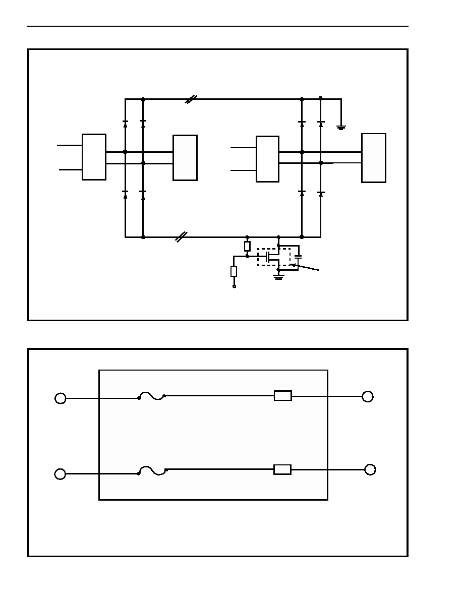
Protection Circuit Design
The high voltage protection circuit is the MH80625C
which can be used in conjunction with the
MH89625C to meet the CCITT K.20 specification.
See Figures 3 and 4. The protection circuit consists
of 1 MOSFET Transistor (BUZ 22) per 16 lines and 4
voltage clamping diodes (IN4004) per line circuit.
This protection circuit will dissipate the lightning and
AC power energy to protect the line circuit. The
Energy Dump Ground (EDG) is tied to the chassis of
the system ground. The PCB E.D.G. track to the
MOSFET must be run separately. The width of the
ground track should be greater than 0.050 thou and
the resistance should be kept as low as possible,
less than 1 ohm. The MOSFET requires a heat sink
of 9∞C/W to dissipate the heat generated by the
overvoltages
Mechanical Data
See Figure 6.

2-281
Preliminary Information
MH89625C
Figure 3 - Typical Line Card Application
Tip
Ring
RF2
RF1
RD4
RD1
RD2
RD3
VRLY
VDD
VEE
AGND RGND
LCA
V
Bat
LGND
VAC
SHK
LED
GS
DSTi
DSTo
C2i
CA
CSTi
F1i
VREF
TOUT
ROUT
TIN
RIN
Test
Out
Test
In
Tip
Ring
K4A
K4B
K3A
K3B
8
3
5
6
K1B
K2B
K1A
K2A
D1
D2
D3
D4
C1
R1
R2
Q1
to other
circuit
Heat sink 9
o
C/W
1
2
7
8
22
20
19
21
23
31
9
30
18
17
12
16
24
14
15
13
35
11
10
34
36
37
32
-48V
90
VRMS
25Hz
PTC
-48V
290V
TISP
-5V
K4 RELAY
K1 RELAY
K2 RELAY
K3 RELAY
+5V
-5V
Components
D1,D2,D3,D4 IN4004
Q1 = FET BUZ 22 or equivalent
R1 = 10k
+5% 1/4W
R2 = 1k
+ 5% 1/4W
C1 = 0.01
µ
F + 10% 100V
PTC = 55
, 50mA
MH89625C
MH80625C
-48V
2-282
MH89625C
Preliminary Information
Figure 4 - 16 Lines Circuit Configuration
Figure 5 - Solid State External Protection Application Circuit
IN4004
IN4004
IN4004
IN4004
TIP
RING
Heat Sink
9
o
C/w
10nF/100V
10K
1K
-48V
E.D.G
TIP
RING
TOUT
ROUT
TOUT
ROUT
TIP1
RING1
LINE 1
MH80625C
MH89625C
MH80625C
MH89625C
TIP 16
RING 16
LINE 16
8
3
5
6
1
2
5
6
1
2
Energy Dump Ground (E.D.G)
3
8
G
S
D
F1
F2
R1
R2
Tip
Ring
To Tip and Ring
of
Telephone Line
Tip
Ring
To Tip and Ring
of
SLIC Circuitry
Notes
1) F1, 2
1
/
4
W 250V Slow Blow Fuse (Littlefuse 229.250 or 230.250).
2) R1, 2 5ohm 5% 1W Carbon Composition Resistor.
3) This protection circuit is available as a hybrid circuit with Mitel part number MH80625C.
MH80625C
Protection Circuit
2-283
Preliminary Information
MH89625C
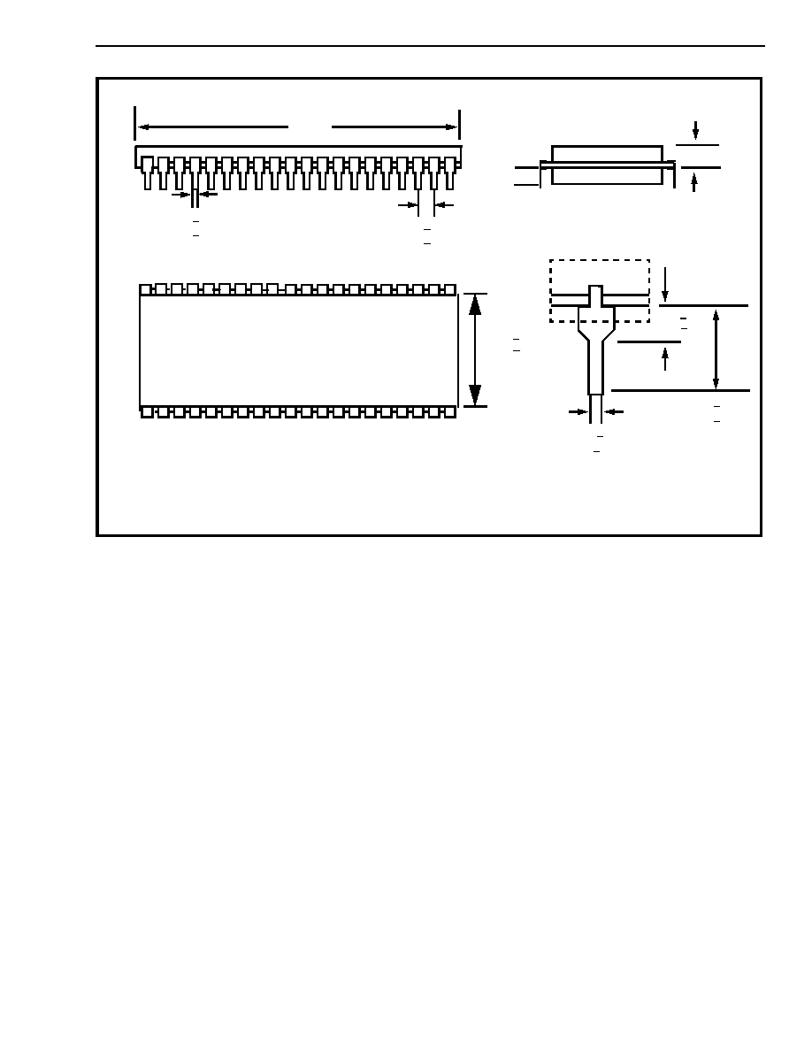
Figure 6 - Mechanical Data
AAAA
AAAA
AAAA
AAAA
AAAA
AAAA
AAAA
AAAA
AAAA
AAAA
AAAA
AAAA
AAAA
AAAA
AAAA
AAAA
AAAA
AAAA
AAAA
AAAA
AAA
AAA
AAA
AAA
AAAA
AAAA
AAAA
AAAA
AAAA
AAAA
AAAA
AAAA
AAAA
AAAA
AAAA
AAAA
AAAA
AAAA
AAAA
AAAA
AAAA
AAAA
AAAA
AAAA
AAAA
AAAA
AAAA
AAAA
AAAA
AAAA
AAAA
AAAA
AAAA
AAAA
AAAA
AAAA
AAAA
AAAA
AAAA
AAAA
AAAA
AAAA
AAAA
AAAA
AAAA
AAAA
AAAA
AAAA
AAAA
AAAA
MH89625C
Notes:
1) Row pitch is to the centre of the pins.
2) All dimensions are typical and in inches (mm).
3) Not to scale.
0.10 + 0.01
(2.5 + 0.2)
0.180 (4.5)
0.020 + 0.002
(0.51 + 0.051)
0.08
(2.0)
2.0
(50.8)
0.20 + 0.01
(5.0 + 0.2)
1.30 +0.03
(33.0+0.8)
(7.8 +0.5)
0.30 +0.02
0.020 + 0.005
(0.51 + 0.13)
Note 1
AAAA
AAAA
AAAA
AAAA
AAAA
AAAA
AAAA
AAAA
AAAA
AAAA
AAAA
AAAA
AAAA
AAAA
AAAA
AAAA
AAAA
AAAA
AAAA
AAAA
AAAA
AAAA
AAAA
AAAA
AAAA
AAA
AAA
AAA
AAA
AAA

2-284
MH89625C
Preliminary Information
Notes: