 | –≠–ª–µ–∫—Ç—Ä–æ–Ω–Ω—ã–π –∫–æ–º–ø–æ–Ω–µ–Ω—Ç: MT8840AS | –°–∫–∞—á–∞—Ç—å:  PDF PDF  ZIP ZIP |

5-3
Æ
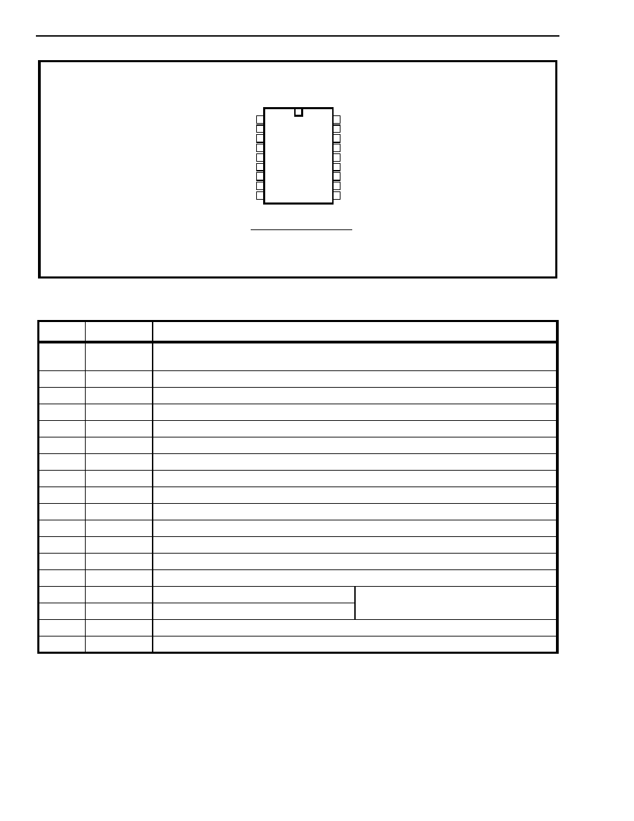
MT8840
Data Over Voice Modem
Features
∑
Performs ASK (amplitude shift keyed)
modulation and demodulation
∑
32 kHz carrier frequency
∑
Up to 2 kbit/s full duplex data transfer rate
∑
On-chip oscillator
∑
On-chip tone caller for alerting functions
∑
Adjustable tone caller frequencies
∑
Selectable self-loop test mode
∑
5V/2.5mA power supply
∑
ISO
2
-CMOS and switched capacitor
technologies
∑
18 Pin DIP
Applications
∑
Simultaneous data and voice communication in
PABXs
∑
2 kbit/s data modem
∑
"Smart" telephone sets
Description
The MT8840 is a carrier over voice modem which
allows simultaneous transfer of voice and data over
a single pair of wires. Data is transferred on an
amplitude shift keyed (ASK) 32 kHz carrier. On-chip
filters remove voice frequency signals from the
received composite voice and data signal prior to
demodulation. The modulating signal is a bit stream
with a
typical
data rate of 2 kbit/s. In addition, the
device contains a two tone warbler which functions
as a telephone ringer. The device is fabricated in
MITEL's double-poly ISO
2
-CMOS technology
utilizing switched-capacitor techniques.
Ordering Information
MT8840AE
18 Pin Plastic DIP
MT8840AS
18 Pin SOIC
0∞C to +85∞C
Figure 1 - Functional Block Diagram
OSC1
OSC2
CK32
ETC MTC FATC
TxDI
RxDO
DET
CRx
V
DD
V
SS
V
Ref
LOOP
TCO
TxO
RxE
RxI
Timing
and
Control
Tone
Caller
Modulator
TX Bandpass
Filter
TX Post-
Filter
RX Pre-
Filter
R
O
U
T
I
N
AGC
G
RX Bandpass
Filter
Demodulator
ISSUE 4
November 1990
ISO
2
-CMOS
MT8840
ISO
2
-CMOS
5-4
Figure 2 - Pin Connections
Pin Description
Pin #
Name
Description
1
DET
Demodulator detection level adjust input (Analog). Internal resistor divider applies
2.36V in open circuit condition. Connection of external resistor will vary detect level.
2
CRx
External AGC time constant adjust input (Analog). Connect external capacitor to V
SS
.
3
RxI
Modulated receive signal input (Analog). Biased at V
Ref
.
4
RxE
Receive enable input (Digital) with internal pull up. Active high.
5
LOOP
Self-test mode select input (Digital) with internal pull down. Active high.
6
V
Ref
Internal reference supply voltage input (Analog) .
7
TxO
Modulated transmit carrier output (Analog).
8
TxDI
Transmit data input (Digital).
9
V
SS
Negative power supply.
10
FATC
Tone caller center frequency adjust input (Analog).
11
TCO
Tone caller output (Digital).
12
MTC
Mute tone caller input (Digital) with internal pull down. Active high.
13
ETC
Enable tone caller input (Digital) with internal pull down. Active high.
14
CK32
32 kHz data strobe output (Digital).
15
OSC1
Clock Input
3.579545 MHz crystal connected between
these pins completes internal oscillator.
16
OSC2
Clock Output to drive external devices.
17
RxDO
Receive data output (Digital). Synchronized to CK32.
18
V
DD
Positive power supply.
1
2
3
4
5
6
7
8
9
10
18
17
16
15
14
13
12
11
DET
CRx
Rxl
RxE
LOOP
VRef
TxO
TxDI
VSS
VDD
RxDO
OSC2
OSC1
CK32
ETC
MTC
TCO
FATC
18 PIN PLASTIC DIP/SOIC

ISO
2
-CMOS
MT8840
5-5
Functional Description
The MT8840 contains the modulator and
demodulator circuitry for 32 kHz ASK signalling as
well as a two-tone warbler (tone caller) to replace the
function of the mechanical telephone ringer.
A 32 kHz carrier is 100% amplitude modulated by the
digital bit stream applied to input TxDI. This results in
an amplitude shift keyed (ASK) 32 kHz carrier. A
logical high at TxDI disables the carrier and a logical
low enables it. The digitally modulated waveform is
shaped by the Tx BANDPASS FILTER and smoothed
by the Tx POST FILTER. The signal then enters the
routing block where it is transferred to the TxO
output.
The modulated 32 kHz receive signal is applied to
RxI. With a logical low applied to LOOP and a logical
high applied to RxE, receive signals are routed to the
Rx PREFILTER. High frequencies are removed by
the Rx PREFILTER to prevent aliasing in the
switched capacitor Rx BANDPASS FILTER. Voice
signals are removed by the bandpass filter which is
followed by an AGC circuit. This provides a dynamic
range of 20dB for the receiver. An external 1µF
capacitor connected from CRx to V
SS
is required to
control the AGC attack and decay time constants.
Data is recovered from the received signal in the
demodulator. The minimum voltage level to which
the demodulator responds may be adjusted by
connecting a resistor from DET to V
DD
or V
Ref
. Since
DET is the input to a comparator, noise should be
kept to a minimum at this pin. The recovered receive
data is synchronized to the leading edge of the 32
kHz clock (available at CK32) before appearing at
RxDO.
When in loop around mode, the Rx PREFILTER
input is internally disconnected from the RxI input pin
and connected to TxO. The transmitter output is still
available at TxO.
A two tone warbling audio signal is available at TCO
when the tone caller enable input (ETC) is high. TCO
is internally clamped to V
Ref
when the tone caller is
disabled. The tone output can be attenuated by 20dB
if a logical high is applied to the tone caller mute
input (MTC).
Applications
Figures 3 through 5 show how the MT8840 may be
utilized to transfer data and voice simultaneously
over a single pair of wires in digital or analog PABXs
and "smart" telephone sets. In all three figures a
microprocessor sends/receives data to/from the
MT8840 via a UART which converts the data format
from parallel-to-serial or serial-to-parallel for the
transmit and receive directions, respectively. In the
receive direction the MT8840 has on-board filters to
reject voice-band signals leaving only the 32 kHz
carrier. This carrier is then demodulated to recover
the received data. In the transmit direction the data
to be sent is modulated and passed on to a summing
circuit which sums the modulated 32 kHz carrier and
voiceband signals for transmission over the
telephone line. In the PABX the Filter/Codec has
filters which reject the 32 kHz carrier from the
received composite voice and data signal allowing
only voiceband signals to pass through which are
then PCM encoded for digital switching. However, in
both the analog PABX and smart telephone set,
lowpass filters could be included to bandlimit the
received signal leaving only voice signals to be
passed on to the switch array or handset earpiece.

MT8840
ISO
2
-CMOS
5-6
Figure 3 - Digital PABX Block Diagram
Figure 4 - Analog PABX Block Diagram
Micro-
processor
UART
Tx Data
Rx Data
Tx
Rx
Summing
Circuit
2W/4W
Converter
Telephone
line
PCM
Highway
MT8840
FILTER/
CODEC
(MT896X)
Tx
Rx
Micro-
processor
UART
Tx Data
Rx Data
Tx
Rx
Summing
Circuit
2W/4W
Converter
Telephone
line
(Optional)
Low-
Pass
Filter
Analog
Switch
Array
(MT8804)
Tx
Rx
To
Another
Telephone
Extension
SLIC
MT8840

ISO
2
-CMOS
MT8840
5-7
Figure 5 - Smart Telephone Set Block Diagram
Figure 6 - Crystal Oscillator Connections for Driving Multiple MT8840s
Tx
Rx
Summing
Circuit
Telephone
line
MT8840
Micro-
processor
UART
Tx Data
Rx Data
Low-
Pass
Filter
Handset
(Optional)
2W/4W
Converter
When a single crystal is shared among a number of MT8840 devices, OSC1 and OSC2 should be a.c. coupled with a 1000
pF capacitor as shown above. This capacitor is not needed between the device with the crystal and the first driven device.
A capacitor should be used in the first stage whenever such a chain of devices is driven from a clock instead of a crystal. A
33pF capacitor should be connected between OSC1 and VSS to compensate for the load on OSC2.
V
DD
V
SS
OSC1
OSC2
MT8840
C=33pF
MT8840
OSC1
OSC2
C=1000pF
MT8840
OSC1
OSC2
C=1000pF
∑ ∑ ∑
MT8840
ISO
2
-CMOS
5-8
* Exceeding these ratings may cause permanent damage. Functional operation under these conditions is not implied.
Notes: 1. Voltage specified is generated internally and measured with no external components connected to DET
Absolute Maximum Ratings*
Parameter
Symbol
Min
Max
Unit
1
Supply Voltage
V
DD
-V
SS
-0.3
+7.0
V
2
Voltage On Any Pin
V
Max
V
SS
-0.3
V
DD
+0.3
V
3
Current On Any Pin
I
Max
20
mA
4
Storage Temperature
T
S
-65
+150
∞C
5
Package Power Dissipation
P
Diss
850
mW
Recommended Operating Conditions
Parameter
Symbol
Min
Typ
Max
Unit
1
Operating Supply Voltages
V
DD
4.75
5
5.25
V
2
V
Ref
0.4V
DD
V
3
Operating Supply Currents
I
DD
2.5
5.0
mA
4
I
Ref
200
µA
5
Operating Temperature
T
O
0
+85
∞C
6
Load Capacitance (TxO)
C
L
50
pF
7
Load Resistance (TxO)
R
L
10
K
D.C. Characteristics -
V
DD
= 5.0 V ± 5% V
SS
=0V T = 0 - 85
o
C (All voltages are referenced to V
SS
/GND)
Characteristics
Sym
Min
Typ
Max
Unit
Test Conditions
1
D
I
G
I
T
A
L
I
/
O
Input Current
I
IN
±10
µA
V
IN
= 0 to V
DD
2
Input Low Voltage
V
IL
0
1.5
V
3
Input High Voltage
V
IH
3.5
5.0
V
4
Output Low Voltage
V
OL
0.4
V
I
OL
= 0.4mA
5
Output High Voltage
V
OH
4.6
V
I
OH
= 0.4mA
6
Output Drive Current
7
N Channel Sink (Except OSC2)
I
OL
0.4
mA
V
OL
= 0.4V
8
OSC2
0.1
mA
9
P Channel Source (Except OSC2)
I
OH
0.4
mA
V
OH
= 4.6V
10
OSC2
0.1
mA
11
A
N
A
L
O
G
I
/
O
Input Current (RxI, FATC)
I
IN
±10
µA
V
IN
= 0 to 5.0V
12
Input Resistance (FATC)
R
IN
500
K
13
(DET to V
DD
)
170
K
14
(DET to V
Ref
)
23
K
15
Input Capacitance (RxI)
C
IN
50
pF
16
(FATC)
10
pF
17
Any Digital Input
5.0
7.5
pF
18
Output Resistance (TxO)
R
O
100
19
(TCO)
3
K
MTC = 0
20
(TCO)
30
K
MTC = 1
21
Output Offset Voltage (TxO)
V
O
±25
±200
mV
22
Output Voltage (DET)
V
O
2.20
2.36
2.55
V
See Note 1

ISO
2
-CMOS
MT8840
5-9
Notes:
1.
All A.C. parameters are based on a typical data rate of 2 kbit/s.
2.
Measured with no external resistor to DET input. Detection level internally set to 2.36V typical.
A.C. Characteristics -
V
DD
=5.0V±5% V
SS
=0V T=0 - 85∞C (All voltages are referenced to V
SS
/GND)
Characteristics
Sym
Min
Typ
Max
Unit
Test Conditions
1
D
I
G
I
T
A
L
I
/
O
Crystal/Clock Frequency
f
C
3.5759 3.5795 3.5831
MHz
OSC1, OSC2
2
Clock Input (OSC 1)
3
Rise Time
t
LHCI
100
ns
10% - 90% of (V
DD
- V
SS
)
4
Fall Time
t
HLCI
100
ns
5
Duty Cycle
DC
CI
40
50
60
%
6
Clock Output (OSC 2)
7
Rise Time
t
LHCO
100
ns
C
L
= 30pF, 3.58MHz ext.
8
Fall Time
t
HLCO
100
ns
clock to OSC1
9
Duty Cycle
DC
CO
50
%
10
Capacitive Load
C
LCO
30
pF
11
Clock Output (CK32)
F
C32
32508
32541
32574
Hz
fc = 3.5795MHz
12
Rise Time
t
LH32
100
ns
10% - 90% of (V
DD
- V
SS
)
13
Fall Time
t
HL32
100
ns
C
L
= 100pF
14
Duty Cycle
DC
32
50
%
15
Capacitive Load
C
L32
100
pF
16
T
O
N
E
C
A
L
L
E
R
Warbler Frequency (TCO)
f
W
7.935
7.945
7.955
Hz
fc = 3.5795MHz ± 0.1%
17
Low Tone Frequency
f
LT
352
390
428
Hz
FATC = 0, f
c
= 3.5795MHz
18
1036
1148
1260
Hz
FATC = V
DD
, f
c
= 3.5795MHz
19
High Tone Frequency
f
HT
440
487
535
Hz
FATC = 0, f
c
= 3.5795MHz
20
1295
1434
1574
Hz
FATC = V
DD
, f
c
= 3.5795MHz
21
Harmonic Relationship
f
HT
/f
LT
1.25
22
Warbler Output (TCO)
23
Rise Time
t
LHWO
500
ns
100K
load to V
Ref
24
Fall Time
t
HLWO
500
ns
C
L
= 30pF, MTC = 0
25
Duty Cycle
DC
WO
50
%
26
Output Level (TCO)
V
TCC
V
DD
V
pp
MTC = 0
27
0.625
V
pp
MTC = 1
(100K
load to V
Ref
)
28
M
O
D
U
L
A
T
O
R
Modulated Frequency
f
MOD
32541
Hz
29
Output Level (TxO)
V
TxO
225
250
270
mV
pp
V
DD
= 5V
30
Output Level (TxO)
31
variation vs. V
DD
V
TxO
100
%
32
Transmit Data Input (TxDI)
33
Rise Time
t
LHTxDI
100
ns
34
Fall Time
t
HLTxDI
100
ns
35
Data Rate (TxDI)
f
Data
2
k/bits See Note 1
36
D
E
M
O
D
U
L
A
T
O
R
Input Impedance (RxI)
Z
IN
50
K
32 kHz Input Frequency
37
Valid Input Level - Data (RxI)
V
RxI
40
400
mV
pp
See Note 2
38
Valid Input Level - Data + Voice
V
RxI
3.0
V
pp
39
Receive Data Output (RxDO)
f
Data
2
kbit/s
40
Rise Time
100
ns
10% - 90% of (V
DD
- V
SS
)
41
Fall Time
100
ns
C
L
= 100pF
42
Capacitive Load
100
pF
43
Duty Cycle
40
50
60
%

MT8840
ISO
2
-CMOS
5-10
Notes:
1.
All A.C. parameters are based on a typical data rate of 2 kbit/s.
2.
Measured with no external resistor to DET input. Detection level internally set to 2.36V typical.
A.C. Characteristics (Continued)
Characteristics
Sym
Min
Typ
Max
Unit
Test Conditions
44
D
E
M
O
D
Inband Noise Rejection (S/N)
12
dB
Input Sig. (RxI) = 400mV
pp
45
Attenuation to Voice Signals
40
dB
f
in
= 0 - 5KHz
46
Detect Filter Q
Q
3.8
47
Detector Center Frequency
32
kHz