4-107
Æ
Features
∑
Central office quality DTMF transmitter/
receiver
∑
Low power consumption
∑
High speed adaptive micro interface
∑
Adjustable guard time
∑
Automatic tone burst mode
∑
Call progress tone detection to -30dBm
Applications
∑
Credit card systems
∑
Paging systems
∑
Repeater systems/mobile radio
∑
Interconnect dialers
∑
Personal computers
Description
The MT8889C is a monolithic DTMF transceiver with
call progress filter. It is fabricated in CMOS
technology offering low power consumption and high
reliability.
The receiver section is based upon the industry
standard MT8870 DTMF receiver while the
transmitter utilizes a switched capacitor D/A
converter for low distortion, high accuracy DTMF
signalling. Internal counters provide a burst mode
such that tone bursts can be transmitted with precise
timing. A call progress filter can be selected allowing
a microprocessor to analyze call progress tones.
The MT8889C utilizes an adaptive micro interface,
which allows the device to be connected to a number
of popular microcontrollers with minimal external
logic. The MT8889C-1 is functionally identical to the
MT8889C except the receiver is enhanced to accept
lower level signals, and also has a specified low
signal rejection level.
Ordering Information
MT8889CE/CE-1
20 Pin Plastic DIP
MT8889CC/CC-1
20 Pin Ceramic DIP
MT8889CS/CS-1
20 Pin SOIC
MT8889CN/CN-1
24 Pin SSOP
-40∞C to +85∞C
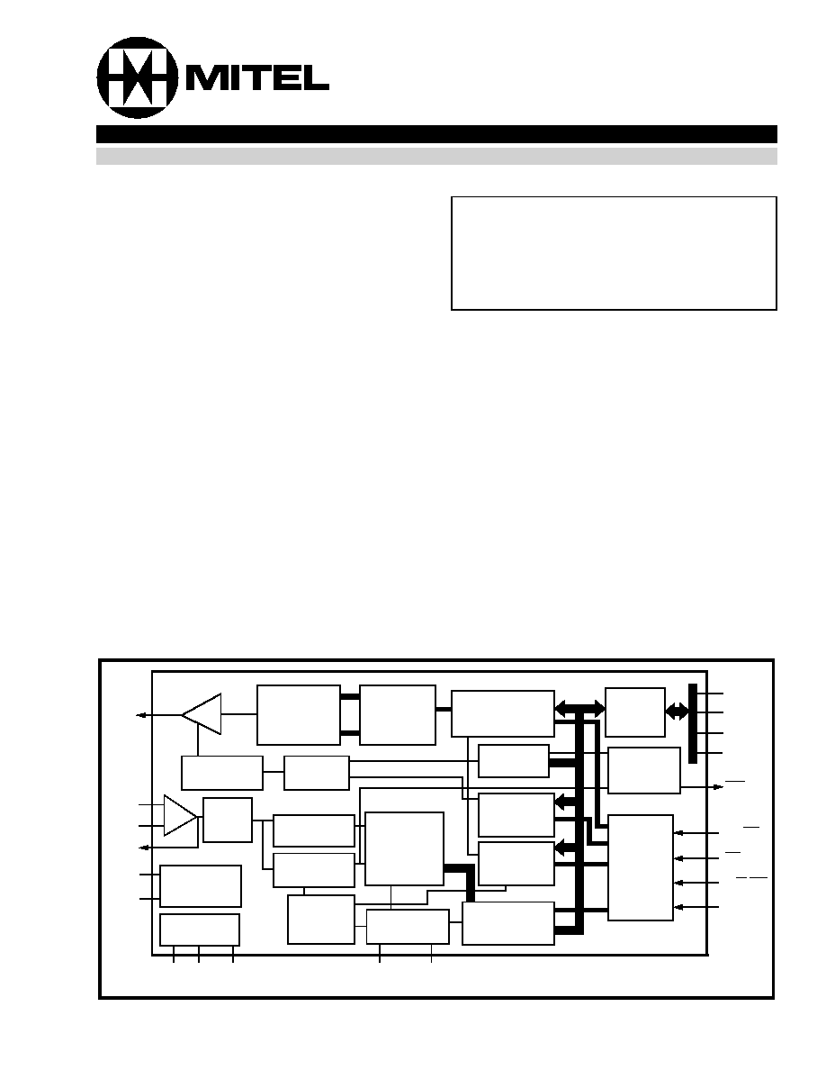
Figure 1 - Functional Block Diagram
TONE
IN+
IN-
GS
OSC1
OSC2
V
DD
V
Ref
V
SS
ESt
St/GT
D0
D1
D2
D3
IRQ/CP
DS/RD
CS
R/W/WR
RS0
D/A
Converters
Row and
Column
Counters
Transmit Data
Register
Data
Bus
Buffer
Tone Burst
Gating Cct.
+
-
Oscillator
Circuit
Bias
Circuit
Control
Logic
Digital
Algorithm
and Code
Converter
Control
Logic
Steering
Logic
Status
Register
Control
Register
A
Control
Register
B
Receive Data
Register
Interrupt
Logic
I/O
Control
Low Group
Filter
High Group
Filter
Dial
Tone
Filter
ISSUE 2
May 1995
MT8889C/MT8889C-1
Integrated DTMF Transceiver
with Adaptive Micro Interface
MT8889C/MT8889C-1
4-108
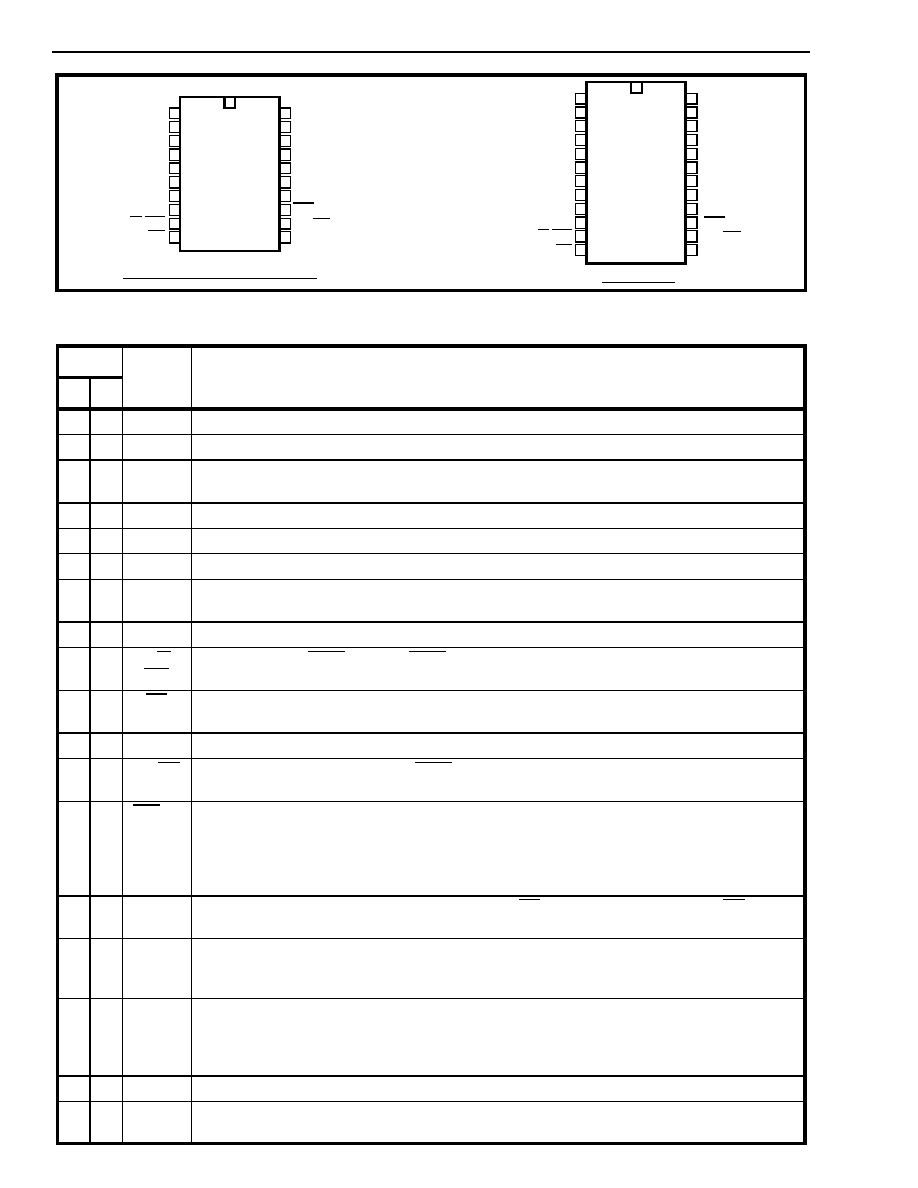
Figure 2 - Pin Connections
Pin Description
Pin #
Name
Description
20
24
1
1
IN+
Non-inverting op-amp input.
2
2
IN-
Inverting op-amp input.
3
3
GS
Gain Select. Gives access to output of front end differential amplifier for connection of
feedback resistor.
4
4
V
Ref
Reference Voltage output (V
DD
/2).
5
5
V
SS
Ground (0V).
6
6
OSC1
Oscillator input. This pin can also be driven directly by an external clock.
7
7
OSC2
Oscillator output. A 3.579545 MHz crystal connected between OSC1 and OSC2 completes
the internal oscillator circuit. Leave open circuit when OSC1 is driven externally.
8
10
TONE
Output from internal DTMF transmitter.
9
11
R/W
(
WR
)
(Motorola) Read/Write or (Intel) Write microprocessor input. TTL compatible.
10
12
CS
Chip Select input. This signal must be qualified externally by either address strobe (AS),
valid memory address (VMA) or address latch enable (ALE) signal, see Figure 12.
11
13
RS0
Register Select input. Refer to Table 3 for bit interpretation. TTL compatible.
12
14
DS
(
RD) (Motorola) Data Strobe or (Intel) Read
microprocessor input. Activity on this input is only
required when the device is being accessed. TTL compatible.
13
15
IRQ/CP Interrupt Request/Call Progress (open drain) output. In interrupt mode, this output goes
low when a valid DTMF tone burst has been transmitted or received. In call progress mode,
this pin will output a rectangular signal representative of the input signal applied at the input
op-amp. The input signal must be within the bandwidth limits of the call progress filter, see
Figure 8.
14-
17
18-
21
D0-D3
Microprocessor data bus. High impedance when CS = 1 or DS =0 (Motorola) or RD = 1
(Intel). TTL compatible.
18
22
ESt
Early Steering output. Presents a logic high once the digital algorithm has detected a valid
tone pair (signal condition). Any momentary loss of signal condition will cause ESt to return
to a logic low.
19
23
St/GT
Steering Input/Guard Time output (bidirectional). A voltage greater than V
TSt
detected at
St causes the device to register the detected tone pair and update the output latch. A
voltage less than V
TSt
frees the device to accept a new tone pair. The GT output acts to
reset the external steering time-constant; its state is a function of ESt and the voltage on St.
20
24
V
DD
Positive power supply (5V typ.).
8,9
16,
17
NC
No Connection.
1
2
3
4
5
6
7
8
9
10
11
12
20
19
18
17
16
15
14
13
IN+
IN-
GS
VRef
VSS
OSC1
OSC2
TONE
R/W/WR
CS
VDD
St/GT
ESt
D3
D2
D1
D0
IRQ/CP
DS/RD
RS0
NC
1
2
3
4
5
6
7
8
9
10
11
12
13
14
15
16
24
23
22
21
20
19
18
17
IN+
IN-
GS
VRef
VSS
OSC1
OSC2
NC
TONE
R/W/WR
CS
VDD
St/GT
ESt
D3
D2
D1
D0
NC
NC
IRQ/CP
DS/RD
RS0
24 PIN SSOP
20 PIN CERDIP/PLASTIC DIP/SOIC
MT8889C/MT8889C-1
4-109
Functional Description
The MT8889C/MT8889C-1 Integrated DTMF
Transceiver consists of a high performance DTMF
receiver with an internal gain setting amplifier and a
DTMF generator, which employs a burst counter to
synthesize precise tone bursts and pauses. A call
progress mode can be selected so that frequencies
within the specified passband can be detected. The
adaptive micro interface allows microcontrollers,
such as the 68HC11, 80C51 and TMS370C50, to
access the MT8889C/MT8889C-1 internal registers.
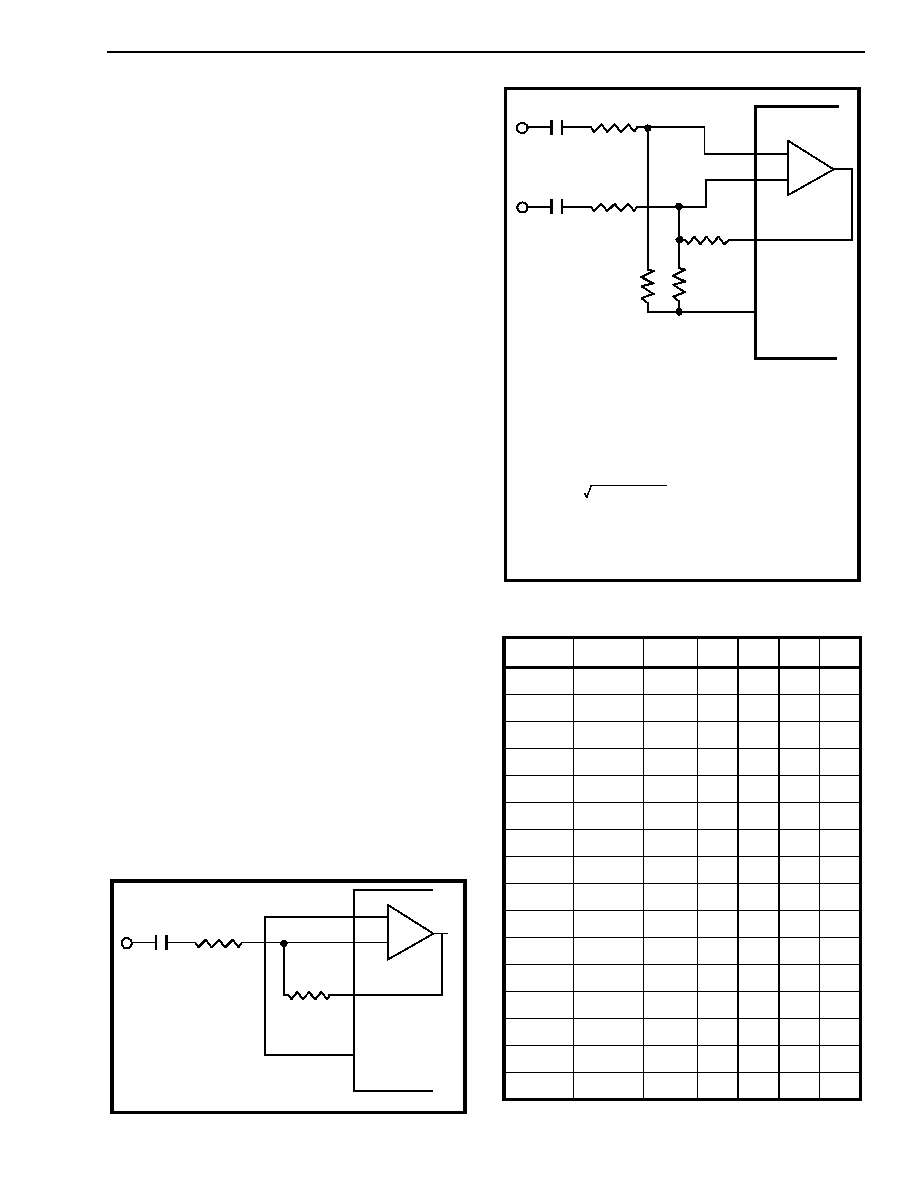
Input Configuration
The input arrangement of the MT8889C/MT8889C-1
provides a differential-input operational amplifier as
well as a bias source (V
Ref
), which is used to bias the
inputs at V
DD
/2. Provision is made for connection of
a feedback resistor to the op-amp output (GS) for
gain adjustment. In a single-ended configuration, the
input pins are connected as shown in Figure 3.
Figure 4 shows the necessary connections for a
differential input configuration.
Receiver Section
Separation of the low and high group tones is
achieved by applying the DTMF signal to the inputs
of two sixth-order switched capacitor bandpass
filters, the bandwidths of which correspond to the low
and high group frequencies (see Table 1). The filters
also incorporate notches at 350 Hz and 440 Hz for
exceptional dial tone rejection. Each filter output is
followed by a single order switched capacitor filter
section, which smooths the signals prior to limiting.
Limiting is performed by high-gain comparators
which are provided with hysteresis to prevent
detection of unwanted low-level signals. The outputs
of the comparators provide full rail logic swings at
the frequencies of the incoming DTMF signals.
Figure 3 - Single-Ended Input Configuration
C
R
IN
R
F
IN+
IN-
GS
V
Ref
VOLTAGE GAIN
(A
V
) = R
F
/ R
IN
MT8889C/
MT8889C-1
Figure 4 - Differential Input Configuration
0= LOGIC LOW, 1= LOGIC HIGH
Table 1. Functional Encode/Decode Table
F
LOW
F
HIGH
DIGIT
D
3
D
2
D
1
D
0
697
1209
1
0
0
0
1
697
1336
2
0
0
1
0
697
1477
3
0
0
1
1
770
1209
4
0
1
0
0
770
1336
5
0
1
0
1
770
1477
6
0
1
1
0
852
1209
7
0
1
1
1
852
1336
8
1
0
0
0
852
1477
9
1
0
0
1
941
1336
0
1
0
1
0
941
1209
*
1
0
1
1
941
1477
#
1
1
0
0
697
1633
A
1
1
0
1
770
1633
B
1
1
1
0
852
1633
C
1
1
1
1
941
1633
D
0
0
0
0
C1
C2
R1
R2
R3
R4
R5
IN+
IN-
GS
V
Ref
MT8889C/
DIFFERENTIAL INPUT AMPLIFIER
C1 = C2 = 10 nF
R1 = R4 = R5 = 100 k
R2 = 60k
, R3 = 37.5 k
R3 = (R2R5)/(R2 + R5)
VOLTAGE GAIN
(A
V
diff) - R5/R1
INPUT IMPEDANCE
(Z
IN
diff) = 2
R1
2
+ (1/
C)
2
MT8889C-1

MT8889C/MT8889C-1
4-110
Following the filter section is a decoder employing
digital counting techniques to determine the
frequencies of the incoming tones and to verify that
they correspond to standard DTMF frequencies. A
complex averaging algorithm protects against tone
simulation by extraneous signals such as voice while
providing tolerance to small frequency deviations
and variations. This averaging algorithm has been
developed to ensure an optimum combination of
immunity to talk-off and tolerance to the presence of
interfering frequencies (third tones) and noise. When
the detector recognizes the presence of two valid
tones (this is referred to as the "signal condition" in
some industry specifications) the "Early Steering"
(ESt) output will go to an active state. Any
subsequent loss of signal condition will cause ESt to
assume an inactive state.
Steering Circuit
Before registration of a decoded tone pair, the
receiver checks for a valid signal duration (referred
to as character recognition condition). This check is
performed by an external RC time constant driven by
ESt. A logic high on ESt causes v
c
(see Figure 5) to
rise as the capacitor discharges. Provided that the
signal condition is maintained (ESt remains high) for
the validation period (t
GTP
), v
c
reaches the threshold
(V
TSt
) of the steering logic to register the tone pair,
latching its corresponding 4-bit code (see Table 1)
into the Receive Data Register. At this point the GT
output is activated and drives v
c
to V
DD
. GT
continues to drive high as long as ESt remains high.
Finally, after a short delay to allow the output latch to
settle, the delayed steering output flag goes high,
signalling that a received tone pair has been
registered. The status of the delayed steering flag
can be monitored by checking the appropriate bit in
the status register. If Interrupt mode has been
selected, the IRQ/CP pin will pull low when the
delayed steering flag is active.
The contents of the output latch are updated on an
active delayed steering transition. This data is
presented to the four bit bidirectional data bus when
the Receive Data Register is read. The steering
circuit works in reverse to validate the interdigit
pause between signals. Thus, as well as rejecting
signals too short to be considered valid, the receiver
will tolerate signal interruptions (drop out) too short
to be considered a valid pause. This facility, together
with the capability of selecting the steering time
constants externally, allows the designer to tailor
performance to meet a wide variety of system
requirements.
Figure 5 - Basic Steering Circuit
Guard Time Adjustment
The simple steering circuit shown in Figure 5 is
adequate for most applications. Component values
are chosen according to the following inequalities
(see Figure 7):
t
REC
t
DPmax
+ t
GTPmax
- t
DAmin
t
REC
t
DPmin
+ t
GTPmin
- t
DAmax
t
ID
t
DAmax
+ t
GTAmax
- t
DPmin
t
DO
t
DAmin
+ t
GTAmin
- t
DPmax
The value of t
DP
is a device parameter (see AC
Electrical Characteristics) and t
REC
is the minimum
signal duration to be recognized by the receiver. A
value for C1 of 0.1 µF is recommended for most
Figure 6 - Guard Time Adjustment
V
DD
V
DD
St/GT
ESt
C1
Vc
R1
MT8889C/
t
GTA
= (R1C1) In (V
DD
/ V
TSt
)
t
GTP
= (R1C1) In [V
DD
/ (V
DD
-V
TSt
)]
MT8889C-1
V
DD
St/GT
ESt
V
DD
St/GT
ESt
C1
R1
R2
C1
R1
R2
t
GTA
= (R1C1) In (V
DD
/V
TSt
)
t
GTP
= (R
P
C1) In [V
DD
/ (V
DD
-V
TSt
)]
R
P
= (R1R2) / (R1 + R2)
t
GTA
= (R
p
C1) In (V
DD
/V
TSt
)
t
GTP
= (R1C1) In [V
DD
/ (V
DD
-V
TSt
)]
R
P
= (R1R2) / (R1 + R2)
a) decreasing tGTP; (tGTP < tGTA)
b) decreasing tGTA; (tGTP > tGTA)

MT8889C/MT8889C-1
4-111
applications, leaving R1 to be selected by the
designer. Different steering arrangements may be
used to select independent tone present (t
GTP
) and
tone absent (t
GTA
) guard times. This may be
necessary to meet system specifications which place
both accept and reject limits on tone duration and
interdigital pause. Guard time adjustment also allows
the designer to tailor system parameters such as talk
off and noise immunity.
Increasing t
REC
improves talk-off performance since
it reduces the probability that tones simulated by
speech will maintain a valid signal condition long
enough to be registered. Alternatively, a relatively
short t
REC
with a long t
DO
would be appropriate for
extremely noisy environments where fast acquisition
time and immunity to tone drop-outs are required.
Design information for guard time adjustment is
shown in Figure 6. The receiver timing is shown in
Figure 7 with a description of the events in Figure 9.
Call Progress Filter
A call progress mode, using the MT8889C/
MT8889C-1, can be selected allowing the detection
of various tones, which identify the progress of a
telephone call on the network. The call progress
tone input and DTMF input are common, however,
call progress tones can only be detected when CP
mode has been selected. DTMF signals cannot be
detected if CP mode has been selected (see Table
7). Figure 8 indicates the useful detect bandwidth of
the call progress filter. Frequencies presented to the
input, which are within the `accept' bandwidth limits
of the filter, are hard-limited by a high gain
comparator with the IRQ/CP pin serving as the
output. The squarewave output obtained from the
schmitt trigger can be analyzed by a microprocessor
or counter arrangement to determine the nature of
the call progress tone being detected. Frequencies
which are in the `reject' area will not be detected and
consequently the IRQ/CP pin will remain low.
Figure 8 - Call Progress Response
AAAA
AAAA
AAAA
AAAA
AAAA
AAAA
AAAA
AAAA
AAAA
AAAA
AAAA
AAAA
AAAA
AAAA
AAAA
AAAA
AAAA
AAAA
AAAA
AAAA
AAAA
AAAA
AAAA
AA
AA
AA
AA
LEVEL
(dBm)
FREQUENCY (Hz)
-25
0
250
500
750
= Reject
= May Accept
= Accept
Figure 7 - Receiver Timing Diagram
V
in
ESt
St/GT
RX
0
-RX
3
b3
b2
Read
Status
Register
IRQ/CP
EVENTS
A
B
C
D
E
F
t
REC
t
REC
t
ID
t
DO
TONE #n
TONE
#n + 1
TONE
#n + 1
t
DP
t
DA
t
GTP
t
GTA
t
PStRX
t
PStb3
DECODED TONE # (n-1)
# n
# (n + 1)
V
TSt